2K 3-Wire CMOS Serial EEPR O M
Features
•
Operating voltage V
–
Read: 2.0V~5.5V
–
Write: 2.4V~5.5V
•
Low power consumption
–
Operating: 5mA max.
–
Standby: 10µA max.
•
User selectable internal organization
–
2K(HT93LC56): 256×8 or 128×16
•
3-wire Serial Interface
•
Write cycle time: 5ms max.
General Description
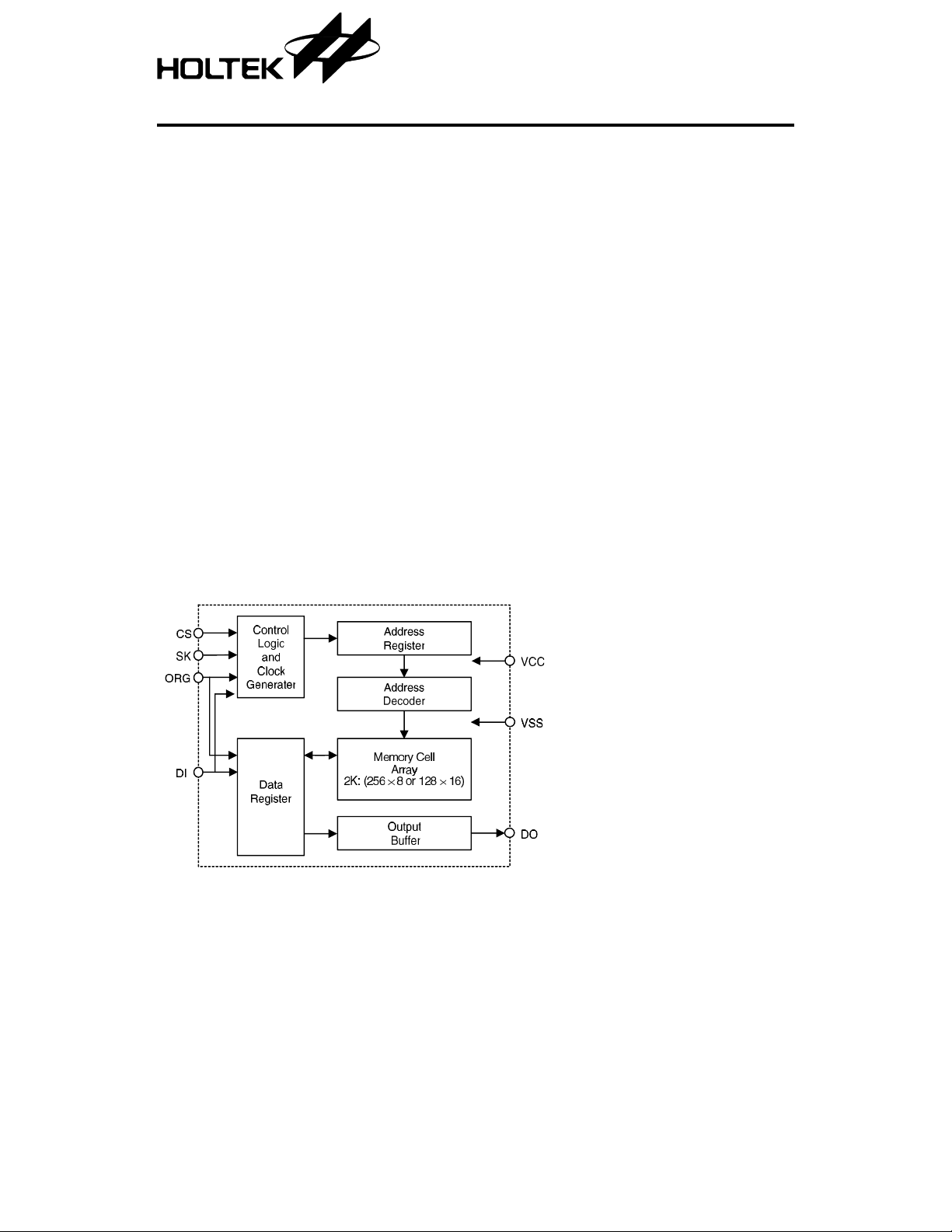
The HT93LC56 is a 2K-bit low voltage nonvolatile, serial electrically erasable programmable
read only memory device using the CMOS floating gate process. Its 2048 bits of memory are
organized into 128 words of 16 bits each when the
ORG pin is connected to VCC or organized into
256 words of 8 bits each when it is tied to VSS. The
CC
HT93LC56
•
Automatic erase-before-write operation
•
Word/chip erase and write operation
•
Write operation with built-in timer
•
Software controlled write protection
•
10-year data retention after 100K rewrite
cycles
•
106 rewrite cycles per word
•
8-pin DIP/SOP package
•
Commercial temp erature range
(0
°C to +70°C)
device is optimized for use in many industrial
and commercial applications where low power
and low voltage operation are essential. By
popular microcontroller, the versatile serial interface including chip select (CS), serial clock
(SK), data input (DI) and data output (DO) can
be easily controlled.
Block Diagram
1 6th May ’99

Pin Assignment
Pin Description
Pin Name I/O Description
CS I Chip select input
SK I Serial clock input
DI I Serial data input
DO O Serial data output
VSS I Negative power supply
ORG I Internal Organization
NC — No connection
VCC I Positive power supply
HT93LC56
2 6th May ’99

HT93LC56
Absolute Maximum Ratings
Operation Temperature (Commercial)..................................................................................0°C to 70°C
Applied V
Applied Voltage on any Pin with Respect to VSS
Supply READ Voltage ...................................... .... .... .... .... .... .... .... .... .... .... .... .... .... .... .... .... .... ....2V to 5.5V
Note: These are stress ratings only. Stresses exceeding the range speci fied under “Absolute Ma xi-
D.C. Characteristics
Voltage with Respect to VSS.......................... .. .... .. .. .... .. .. .... .. .. .... .. .. .... .. .. .... .–0.3V to 6.0V
CC
............................................................VSS
–0.3V to VCC+0.3V
mum Ratings” may cause substantial damage to the device. Functional operation of this
device at other conditions beyond those listed in the specification is not implied and
prolonged exposure to extreme conditions may affect device reliability.
Symbol Parameter
V
I
I
I
I
I
V
V
V
V
C
C
Operating Voltage —
CC
Operating Current
CC1
(TTL)
Operating Current
CC2
(CMOS)
Standby Current
STB
(CMOS)
Input Leakage Current 5V VIN=VSS~V
LI
Output Leakage
LO
Current
Input Low Voltage
IL
Input High Voltage
IH
Output Low Voltage
OL
Output High Voltage
OH
Input Capacitance — VIN=0V, f=250kHz — — 5 pF
IN
Output Capacitance — V
OUT
Test Conditions
V
CC
Conditions
Min. Typ. Max. Unit
Read 2.0 — 5.5 V
Write 2.4 — 5.5 V
5V DO unload, SK=1MHz — — 5 mA
5V DO unload, SK=1MHz — — 5 mA
2~5.5V DO unload, SK=250kHz — — 5 mA
5V CS=SK=DI=0V — — 10
0—1
0—1
5V
V
OUT=VSS~VCC
CS=0V
CC
µA
µA
µA
5V — 0 — 0.8 V
2~5.5V — 0 — 0.1V
5V — 2 — V
2~5.5V — 0.9V
5V I
2~5.5V
5V
2~5.5V
=2.1mA — — 0.4 V
OL
=10µA
I
OL
=–400µA
I
OH
=–10µA
I
OH
=0V, f=250kHz — — 5 pF
OUT
——0.2V
2.4 — — V
V
CC
—VCCV
CC
–0.2 — — V
CC
CC
V
V
3 6th May ’99
 Loading...