Features
Operating voltage: 2.5V~5.5V
·
Minimal external components
·
No external filter is required
·
Low standby current (on power down mode)
·
Excellent performance
·
General Description
The HT9170 series are Dual Tone Multi Fre
quency (DTMF) receivers integrated with digi
tal decoder and bandsplit filter functions. The
HT9170B and HT9170D types supply
power-down mode and inhibit mode operations.
All types of the HT9170 series use digital count
ing techniques to detect and decode all the 16
Selection Table
HT9170
DTMF Receiver
Tristate data output for mC interface
·
3.58MHz crystal or ceramic resonator
·
1633Hz can be inhibited by the INH pin
·
HT9170B: 18-pin DIP package
·
HT9170D: 18-pin SOP package
DTMF tone pairs into a 4-bit code output.
-
Highly accurate switched capacitor filters are
employed to divide tone (DTMF) signals into
low and high group signals. A built-in dial tone
rejection circuit is provided to eliminate the
need for pre-filtering.
Function
Part No.
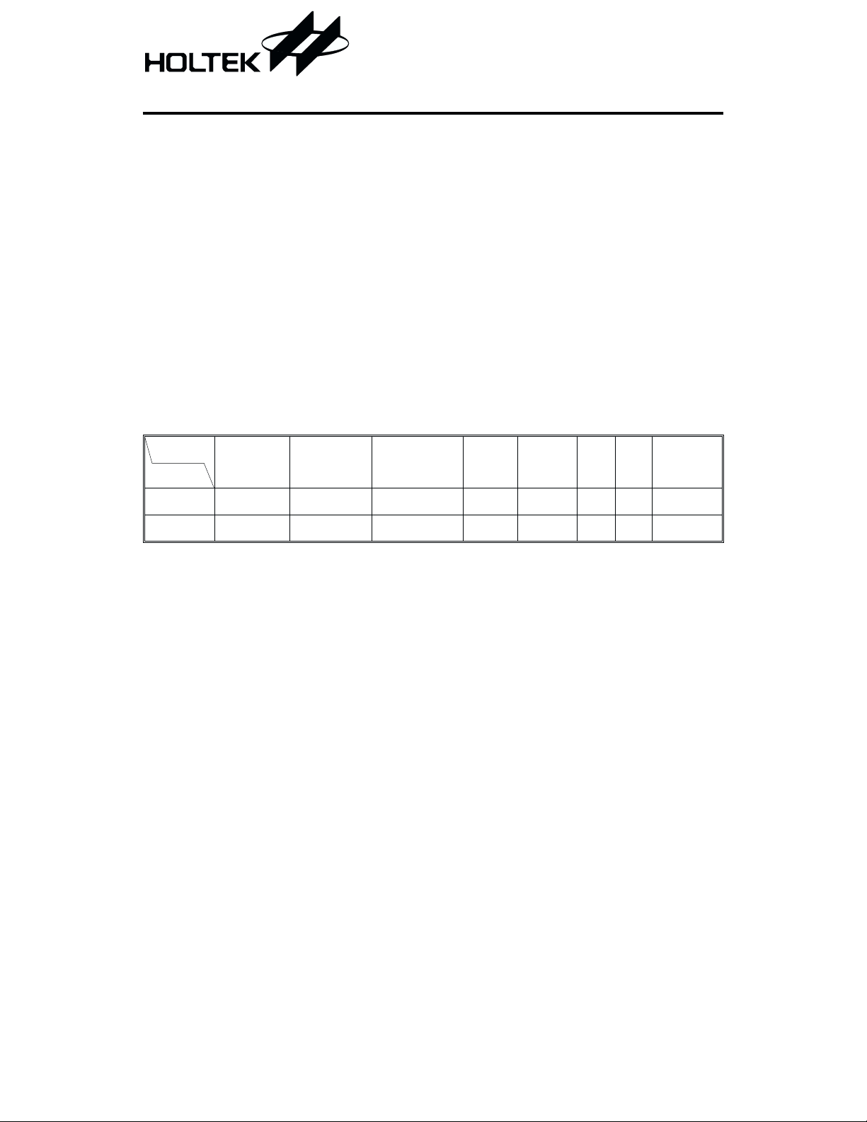
HT9170B 2.5V~5.5V 3.58MHz
HT9170D 2.5V~5.5V 3.58MHz
Operating
Voltage
OSC
Frequency
Tristate
Data Output
ÖÖÖÖ¾
ÖÖÖÖ¾
Power
Down
1633Hz
Inhibit
DV DVB Package
18 DIP
18 SOP
1 December 20, 1999

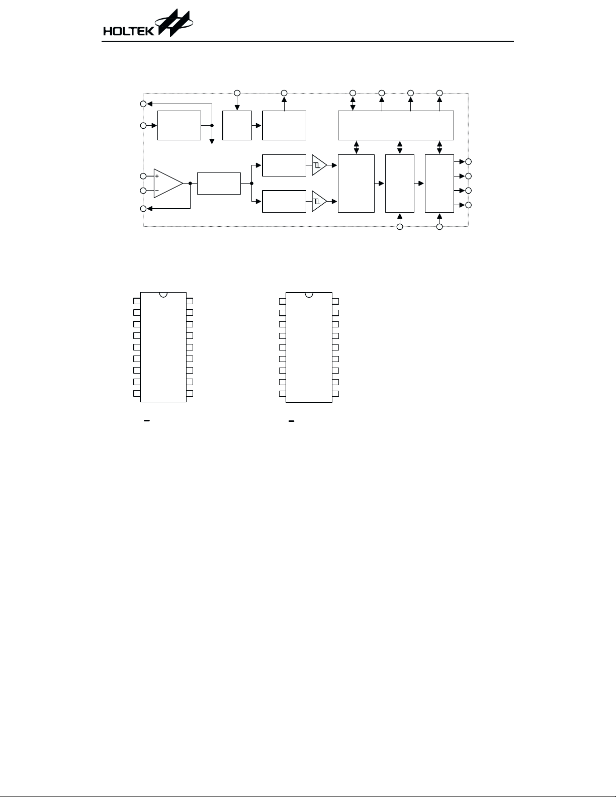
Block Diagram
HT9170
X2
3.58M H z
X1
VP
VN
GS
C rystal
O s c illa to r
OPA
Pin Assignment
VP
VN
GS
VREF
IN H
PW DN
X1
X2
VSS
1
2
3
4
5
6
7
8
9
H T 9170B
18
17
16
15
14
13
12
11
10
1 8 D IP
Pre -Filter
VDD
RT/GT
EST
DV
D3
D2
D1
D0
OE
PW DN DVB
Bias
Circuit
VREF RT/GT EST DV
Low G roup
H igh G roup
VP
VN
GS
VREF
IN H
PW DN
X1
X2
VSS
Vref
G enerator
F ilte r
Filter
1
2
3
4
5
6
7
8
9
18
17
16
15
14
13
12
11
10
Steering C ontrol C ircuit
Frequency
Detector
VDD
RT/GT
EST
DV
D3
D2
D1
D0
OE
C ode
Detector
IN H
Latch
&
Output
Buffer
OE
H T 9170D
1 8 S O P
D0
D1
D2
D3
2 December 20, 1999

Pin Description
HT9170
Pin Name I/O
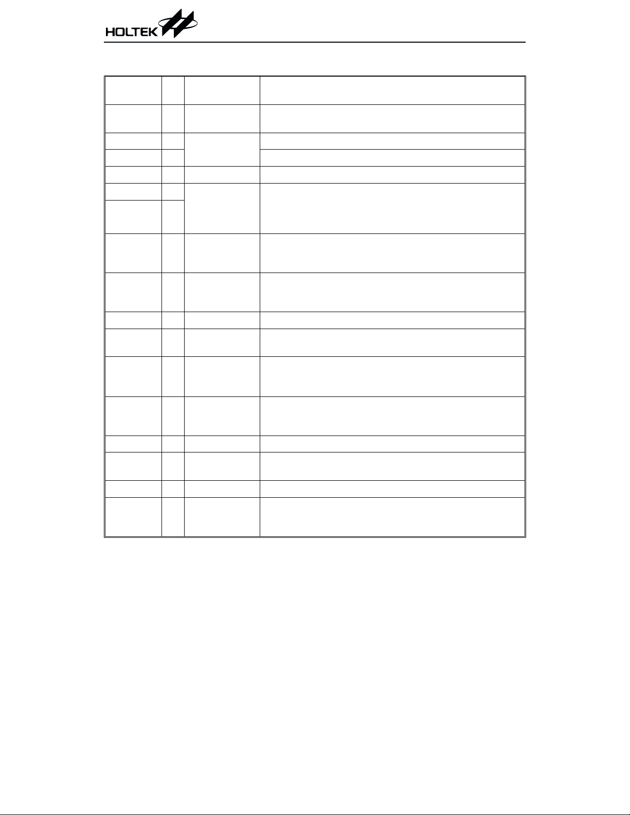
VP I
VN I Operational amplifier inverting input
GS O Operational amplifier output terminal
VREF O VREF Reference voltage output, normally V
X1 I
X2 O
PWDN I
INH I
VSS
OE I
D0~D3 O
DV O CMOS OUT
EST O CMOS OUT Early steering output (see Functional Description)
RT/GT I/O CMOS IN/OUT
VDD
DVB O CMOS OUT
¾¾
¾¾
Internal
Connection
OPERATIONAL
AMPLIFIER
OSCILLATOR
CMOS IN
Pull-low
CMOS IN
Pull-low
CMOS IN
Pull-high
CMOS OUT
Tristate
Description
Operational amplifier non-inverting input
/2
DD
The system oscillator consists of an inverter, a bias resistor
and the necessary load capacitor on chip.
A standard 3.579545MHz crystal connected to X1 and X2 ter
minals implements the oscillator function.
Active high. This enables the device to go into power down
mode and inhibits the oscillator. This pin input is internally
pulled down.
Logic high. This inhibits the detection of tones representing
characters A, B, C and D. This pin input is internally pulled
down.
Negative power supply
D0~D3 output enable, high active
Receiving data output terminals
OE=²H²: Output enable
OE=²L²: High impedance
Data valid output
When the chip receives a valid tone (DTMF) signal, the DV
goes high; otherwise it remains low.
Tone acquisition time and release time can be set through
connection with external resistor and capacitor.
Positive power supply, 2.5V~5.5V for normal operation
One-shot type data valid output, normal high, when the chip
receives a valid time (DTMF) signal, the DVB goes low for
10ms.
-
3 December 20, 1999

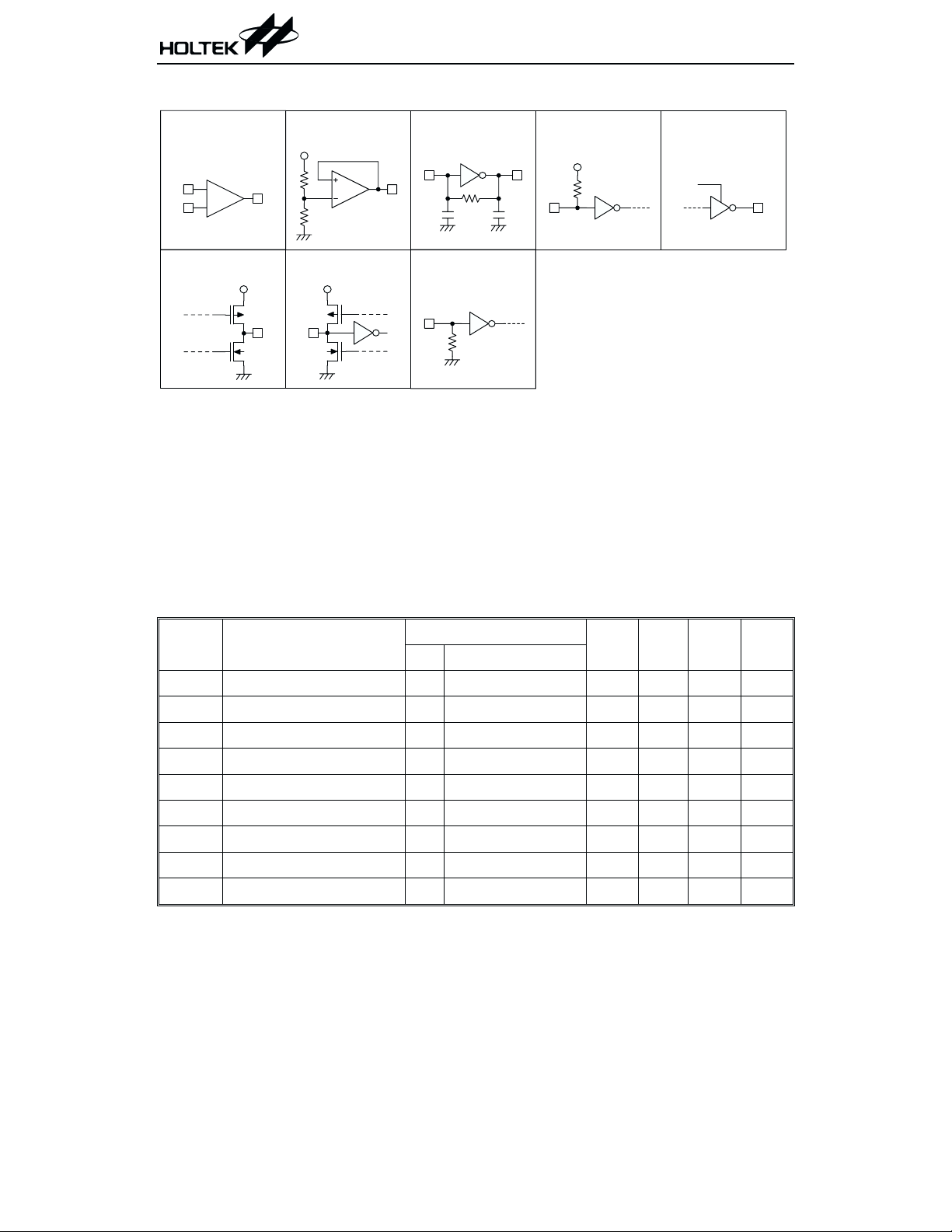
Approximate internal connection circuits
HT9170
OPERATION AL
AM PLIFIER
V-
VN
OPA
V+
VP
CMOS OUT
GS
VREF
OPA
CMOS IN/OUT
O SC ILLA TO R
X1
20pF
CMOS IN
Pull-low
10M
X2
10pF
CMOS IN
Pull-high
CMOS OUT
Tristate
EN
Absolute Maximum Ratings
Supply Voltage.................................-0.3V to 6V
Input Voltage .................V
-0.3V to VDD+0.3V
SS
Note: These are stress ratings only. Stresses exceeding the range specified under ²Absolute Maxi
mum Ratings² may cause substantial damage to the device. Functional operation of this device
at other conditions beyond those listed in the specification is not implied and prolonged exposure to extreme conditions may affect device reliability.
Storage Temperature.................-50°Cto125°C
Operating Temperature ..............-20°Cto75°C
-
D.C. Characteristics
Symbol Parameter
V
I
I
V
V
I
I
R
R
DD
STB
IL
IH
Operating Voltage
DD
Operating Current 5V
Standby Current 5V PWDN=5V
²Low² Input Voltage
IL
²High² Input Voltage
IH
²Low² Input Current
²High² Input Current
Pull-high Resistance (OE) 5V
OE
Input Impedance (VN, VP) 5V
IN
Test Conditions
V
DD
Conditions
¾¾
¾¾
5V
5V
5V
5V
V
VP=VVN
V
VP=VVN
V
OE
¾¾¾
¾
=0V
=5V
=0V
¾¾10¾ MW
4 December 20, 1999
Ta=25°C
Min. Typ. Max. Unit
2.5 5 5.5 V
3.0 7 mA
¾
10 25
mA
1.0 V
4.0
¾¾
¾¾
¾¾
0.1
0.1
60 100 150
V
mA
mA
kW
 Loading...