


HT9015
Preliminary
RF Single Chip for Cordless Phone
Features
Operating voltage: 2.7V~6V
·
Extremely low power consumption current
·
-
ICC=0mA (typ.) in battery-saving mode
-
ICC= 8.5mA (typ.) in standby mode
-
ICC= 13.5mA (typ.) for communication
Built-in IF decoder, compander and PLL
·
IF decoder
·
-
1st/2nd Mixers, RX VCO
-
RSSI quadrature detector, IF AMP
-
Noise detector
General Description
The HT9015 is an RF single chip for cordless
phone systems. Internally these are three major
parts, a PLL, an IF decoder and a compander.
The PLL provides radio channel selection for
either the transmitter or receiver. Frequency
locking status of the selected channel can be
monitored by a control register.
The IF decoder provides two frequency down
converters that let high frequency signals pass
through a mixer and local oscillator to be lowered for frequency even base band signals. It
also provides an RSSI (receiver signal strength
indicator) function to detect the IF output sig-
Compander
·
-
Expander, Compressor, Limiter
-
Receive AMP, MIC AMP, PRE AMP
PLL
·
-
RX PLL, TX PLL
-
Local oscillator
-
Data latch control
-
Unlock detector
Four threshold variable battery alarms
·
nal strength and built-in noise detector for S/N
quality.
The compander provides better S/N ratio for
audio signal processing.
The HT9015 has a wide-range applications in
FM/FSK, Transmitting/Receiving of VHF
bandwidth including cordless phone, narrow
band voice and data transceiver systems.
The most significant advantage of the HT9015
is in the reduction of many external components making it well suited for cordless phone
baseset, handset radio section.
1 April 10, 2000
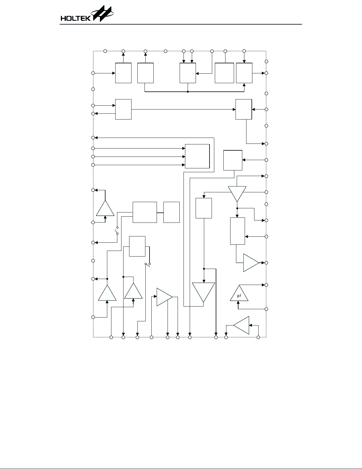
Block Diagram
GND2
6
TX_IN
VCC 3
7
8
LO 1
9
LO 2
CLK
DATA
STB
10
11
12
13
SIG_O UT
Preliminary
VCO 2
48
2
1
RX
VCO
D ata Latch
C ontrol
TX
PLL
LO
RX_OUT
4
TX_O U T
5
OSC
RX
PLL
C_RECT
3
VCO_CONT
VCO 1
47
R egulator
VCC 2
46
Low BAT
Alarm
1STM IX_IN
45
1st
M ix e r
2nd
M ix e r
44
VREF
43
1STM IX_O U T
E_RECT
42
41
2N D M IX _IN
40
N_REC
39
2N D M IX _O U T
38
VCC 1
37
IF _ IN
HT9015
FIL_O U T
FIL_IN
COM P_OUT
C_NF
MIC_OUT
MIC_IN
14
LPF
15
C_M UTE
16
17
18
MIC
AM P
19
PRE_IN
20
PRE_OUT
Com pressor
Expander
E_M UTE
PRE
AM P
21
IF
AM P
Lim iter
Receiver
AM P
25
22
RECE_INEXP_OUT
2423
RO1
RSSI
Quad
Detector
Com -
parator
Data
Com p
28
26
BA T _A LMRO2
27
D_CO M P_OUTRSSI
LPF
Noise
Filter
D_CO M P_IN
36
35
34
33
32
31
30
29
DEC
GND1
IF _ O U T
QUAD
AF_O UT
N_FIL_O UT
N _FIL_IN
2 April 10, 2000
Pin Assignment
Preliminary
HT9015
VCO 2
C_RECT
RX_OUT
TX_O U T
GND2
TX_IN
VCC3
LO 1
LO 2
SIG_OU T
CLK
DATA
STB
FIL_OU T
FIL_IN
COM P_OUT
C_NF
MIC_OUT
MIC_IN
PRE_IN
PRE_OUT
EXP_O U T
RECE_IN
RO1
1
2
3
4
5
6
7
8
9
10
11
12
13
14
15
16
17
18
19
20
21
22
23
24
48
47
46
45
44
43
42
41
40
39
38
37
36
35
34
33
32
31
30
29
28
27
26
25
H T 9 0 1 5
48 SSO P
VCO 1
VCO _CONT
VCC2
1 S T M IX IN
VREF
1STM IX O U T
E_RECT
2 N D M IX IN
N_REC
2N D M IX O U T
VCC1
IF _ IN
DEC
GND1
IF _ O U T
QUAD
AF_O UT
N_FIL_OUT
N _F IL_IN
D_COM P_IN
D_COM P_O UT
RSSI
BAT_ALM
RO2
Pin Description
Pin No. Pin Name I/O Description
1 VCO2 I
2 C_RECT
3 RX_OUT O
4 TX_OUT O
5 GND2
6 TX_IN I
Connects LC network with VCO1 pin to provide the tank circuit
for the received voltage control oscillator
Normally connected to ground through a capacitor.
¾
Receiver phase detector output. The PDT of RX-PLL detects
phase errors from the received PLL. The output is connected to
external low pass filter.
Transmitter phase detector output. The PDT of TX-PLL detects
phase errors from the transmitted PLL. The output is connected
to an external low pass filter.
Digital ground
¾
14-bit programmable transmit counter input. The output signal
from the external VCO circuit can be AC coupled to this pin.
3 April 10, 2000

Preliminary
Pin No. Pin Name I/O Description
7 VCC3
8 LO1 I This pin connects to LO2 pin with external crystal and capacitor.
9 LO2 O
10 SIG_OUT O
11 CLK I Clock input pin
12 DATA I Serial data input pin
13 STB I Data strobe control pin
14 FIL_OUT O Splatter filter output pin
15 FIL_IN I Splatter filter input pin
16 COMP_OUT O Compressor output pin
17 C_NF
18 MIC_OUT O Microphone amplifier output pin
19 MIC_IN I Microphone amplifier input pin
20 PRE_IN I Pre-amplifier input pin
21 PRE_OUT O Pre-amplifier output pin
22 EXP_OUT O Expander output pin
23 RECE_IN I Receiver amplifier input pin
24 RO1 O Receiver amplifier output pin
25 RO2 O Receiver amplifier output pin
26 BAT_ALM O
27 RSSI O
28 D_COMP_OUT O Data comparator output pin
29 D_COMP_IN I
30 N_FIL_IN I Input to noise filter
31 N_FIL_OUT O Output from noise filter
Positive power supply for digital block circuits.
¾
This output pin generates a reference frequency used for the
PLL and the second mixer local oscillator when connected to
LO1 pin with an external crystal and capacitor.
This pin outputs four-type states and is selected by an internal
control register. There are RSSI state and noise state and RX/TX
PLL lock states.
Open drain output.
Normally connected to ground through a capacitor.
¾
Battery alarm output pin. When the battery voltage is lower
than the internal setting threshold this pin is active.
Open drain output.
Receiver signal strength indicator output pin, the output signal
depends on the IF amplifier output signal.
Data comparator input pin. Input to comparator to distinguish
digital data from audio.
HT9015
4 April 10, 2000

Preliminary
Pin No. Pin Name I/O Description
32 AF_OUT O
33 QUAD I
34 IF_OUT O
35 GND1
36 DEC
37 IF_IN I
38 VCC1
39 2NDMIX_OUT O
40 N_REC
41 2NDMIX_IN I
42 E_RECT
43 1STMIX_OUT O
44 VREF O Reference voltage input for compander.
45 1STMIX_IN I
46 VCC2
47 VCO_CONT I Normally connected to ground through a capacitor.
48 VCO1 I
FM demodulator output pin. Output signal frequency is within
the audio band.
Normally provides a 455kHz carry frequency for the FM quadra
ture detector.
IF amplifier output pin. Signal will later pass through external
90°C phase shifter for quadrature detector.
Analog ground
¾
Normally connected to VCC1 through a capacitor.
¾
IF amplifier input pin it is necessary to use the IF filter network
to get high quality IF signal.
Analog power supply
¾
Second mixer IF signal output pin and down converter. IF fre
quency is 455kHz.
Connect to ground through capacitor.
¾
Second mixer RF signal input pin and down converter. Fre
quency is 455kHz.
Expander rectifier filter capacitor pin.
¾
First mixer IF signal output pin and down converter. IF fre
quency is 10.7MHz.
The first mixer RF signal input. Carrier frequency from
20~60MHz.
Directly connects to the two voltage regulators inside.
¾
Connects LC network with VCO2 pin to provide the tank circuit
for the received voltage control oscillator.
HT9015
-
-
-
-
Absolute Maximum Ratings
Supply Voltage ...........................VSS-0.3V to 6V
Input Voltage .................V
Note: These are stress ratings only. Stresses exceeding the range specified under ²Absolute Maxi
mum Ratings² may cause substantial damage to the device. Functional operation of this device
at other conditions beyond those listed in the specification is not implied and prolonged expo
sure to extreme conditions may affect device reliability.
-0.3V to VCC+0.3V
SS
Storage Temperature.................-55°Cto150°C
Operating Temperature ..............-20°Cto70°C
5 April 10, 2000
-
-
Preliminary
HT9015
Electrical Characteristics
Symbol Parameter
V
CC
I
CC1
I
CC2
I
CC3
I
CC4
I
CC5
I
CC(A)
I
CC(BS)
I
REF
V
IH
V
IL
I
IH
I
IL
f
CK
Operating Voltage
Current 1 Consumption 3.6V All on
Current 2 Consumption 3.6V RX-RF ON
Current 3 Consumption 3.6V RX-AF ON
Current 4 Consumption 3.6V TX-RF ON
Current 5 Consumption 3.6V TX-AF ON
Current Alarm Supply 3.6V
Supply Current in Battery
Saving Mode
V
Voltage
REF
Data Input Threshold 3.6V
Data Input Threshold 3.6V
Data Input Current 3.6V
Data Input Current 3.6V
CK Input Frequency 3.6V
Test Conditions
CC
Conditions
V
CC1=VCC3
= 100kW¾
R
L
V
¾
3.6V All off
3.6V
V
IH=VCC
V
= GND
IL
Min. Typ. Max. Unit
¾
¾
¾
¾
¾
¾
¾
¾¾
¾¾
3.6
13.5
8.5
3.5
2.1
1.7
100
0
1.5
V
CC3
¾
¾
¾
¾
¾
¾
¾mA
¾mA
¾
¾
¾¾0¾
¾
¾
¾¾
0
0
¾mA
¾mA
38 1000 kHz
Ta=25°C
V
mA
mA
mA
mA
mA
V
V
V
Regulator
Symbol Parameter
V
REG
I
OUT (MIN)
Output Voltage 3.6V I
Minimum Load Current 3.6V
Detector
Symbol Parameter
V
BAT-L
V
BAT-H
V
BAT-L
V
BAT-H
Detection Voltage 1 3.6V
Detection Voltage 1 3.6V
Detection Voltage 2 3.6V
Detection Voltage 2 3.6V
Test Conditions
Min. Typ. Max. Unit
V
CC
Conditions
= 1mA 1.7 2 2.3 V
OUT
V
OUT=VREG
(Open)-0.05V
¾
3
Test Conditions
Min. Typ. Max. Unit
V
Conditions
CC
¾¾
¾¾
¾¾
¾¾
6 April 10, 2000
3.3
3.37
3.15
3.2
¾
¾
¾
¾
¾
Ta=25°C
mA
Ta=25°C
V
V
V
V

Preliminary
HT9015
Symbol Parameter
V
BAT-L
V
BAT-H
V
BAT-L
V
BAT-H
V
OL
I
LEAK
V
TH
V
OL
I
LEAK
V
TH-H
V
TH-L
V
OL
I
LEAK
V
TH-L
V
TH-H
V
HYS
Detection Voltage 3 3.6V
Detection Voltage 3 3.6V
Detection Voltage 4 3.6V
Detection Voltage 4 3.6V
Output Low Level Voltage 3.6V
Output Leak Current 3.6V
Minimum Detection Level 3.6V f= 500Hz
Output Low Level Voltage 3.6V
Output Leak Current 3.6V
Noise Detection Level 3.6V
Noise Detection Level 3.6V
Noise Detection Level
Voltage
Output Leak Current 3.6V
RSSI Comparator
Detection Voltage
RSSI Comparator
Detection Voltage
RSSI Comparator Hysteresis 3.6V
Test Conditions
Conditions
V
CC
¾¾
¾¾
¾¾
¾¾
I
= 0.1mA
SINK
V
= 3.6V
ALM
I
= 0.2mA
SINK
V
= 3.6V
DATA
¾¾
¾¾
= 0.2mA
I
3.6V
SINK
VSIG= 3.6V
Comparator
3.6V
Output L ® H
Comparator
3.6V
Output H ® L
¾¾
Min. Typ. Max. Unit
¾
¾
3.05
3.10
2.78
2.82
0.1
0
¾
¾
¾
¾
¾
¾mA
¾¾¾
0.1
¾
¾
¾
¾
¾
¾
0.57
0.47
0.1
0.72
0.8
0.08
0
0
¾
¾mA
¾
¾
¾
¾
¾
¾
¾
V
V
V
V
V
mVrms
V
V
V
V
A
m
V
V
V
PLL Detection
Symbol Parameter
f
IN
V
IN
V
LO
I
CP1
I
CP2
I
LEAK
f
LO
Operating Frequency 3.6V
TX-PLL Input Sensitivity 3.6V
Local Oscillator Input
Sensitivity
Charge Pump Output Current 3.6V
Charge Pump Output Current 3.6V
Charge Pump Leak Current 3.6V
Local Oscillator Operating
Frequency
dBmV=dBmV EMF (Open), Ta=25°C
Test Conditions
Min. Typ. Max. Unit
V
3.6V
CC
Conditions
¾¾
¾¾
= 10.240MHz
f
LO
V
= 1.8V
CP
V
= 1.8V
CP
¾
¾
¾
46.61
103
110
200
400
MHz
¾
¾ dBmV
¾ dBmV
¾mA
¾mA
¾¾0¾mA
= 112dBmV
V
3.6V
LO
7 April 10, 2000
¾
10.24
¾
MHz

Preliminary
HT9015
RX-VCO IF + MIX section
(MIX 1)=46.61MHz, fIN(IF)=455kHz, Df=3kHz fm= 1kHz, dBmV=dBmV EMF (Open), Ta=25°C
f
IN
Test Conditions
Symbol Parameter
K
V
V
VCO
Conversion Gain 3.6V
RX VCO Oscillation Level 3.6V
V
CC
Conditions
¾¾1¾
f
= 25~55MHz
VCO
Min. Typ. Max. Unit
110
¾
¾ dBmV
MHz/V
1st and 2nd Mixer, IF AMP
Symbol Parameter
12dB
SINAD
f
MIX1
f
MIX2
G
VC
G
IF
V
OD
12dB SINAD Sensitivity 3.6V
Mixer Operating
Frequency
Mixer Operating
Frequency
Conversion Gain 3.6V Excluding Filter Loss
IF AMP Gain 3.6V
Demodulated Output 3.6V
S/N S/N Ratio 3.6V
AMR AM Rejection Ratio 3.6V
R
IN1
C
IN1
R
IN2
C
IN12
R
IN
R
O1
R
O2
V
RSSI1
V
RSSI2
Input Impedance 3.6V 1st MIX IN
Input Impedance 3.6V 1st MIX IN
Input Impedance 3.6V 2nd MIX IN
Input Impedance 3.6V 2nd MIX IN
Input Resistance 3.6V IF IN
Output Resistance 3.6V 1st MIX OUT
Output Resistance 3.6V 2nd MIX OUT
RSSI Output Voltage 3.6V
RSSI Output Voltage 3.6V
Test Conditions
Min. Typ. Max. Unit
V
CC
Conditions
Input 50W¾20¾ dBmV
3.6V 1STMIXER
3.6V 2NDMIXER
¾
¾
¾
46.61
10.7
26
¾¾75¾
¾
¾
¾
¾
¾
¾
¾
220
55
40
2.1
3.5
5.8
2.5
1.5
330
1.5
1
2.4
(MIX 1)= 70dBmV ¾
V
IN
V
(MIX 1)= 70dBmV ¾
IN
V
(MIX 1)= 70dBmV ¾
IN
(MIX 1)= 20dBmV ¾
V
IN
(MIX 1)= 60dBmV ¾
V
IN
Ta=25°C
MHz
¾
MHz
¾
¾
dB
dB
mVrms
¾
¾
¾
dB
dB
¾ kW
¾
pF
¾ kW
¾
pF
¾ kW
¾W
¾ kW
¾
¾
V
V
8 April 10, 2000

Preliminary
HT9015
Compressor + MIC AMP
Symbol Parameter
V
refc
V
OC
V
4
t
HDC
V
NOC
V
lim1
V
lim2
V
MUTE
Input Reference Level 3.6V
Output Deviation 3.6V
MIC AMP Voltage Gain 3.6V
Total Harmonic Distortion 3.6V
Output Noise Level 3.6V Input-GND Short
Limiting Level 3.6V
Limiting Level 3.6V
Mute Output Level 3.6V
Expander + PRE AMP + Receiver AMP
Symbol Parameter
V
refE
V
OE
G
P3
Input Reference Level 3.6V
Output Deviation 3.6V
PRE AMP Voltage Gain 3.6V
THD1 Total Harmonic Distortion 3.6V
V
MUTE
G
RNG2
G
RNG1
CT
G
S
DR
Mute Output Level 3.6V
PRE AMP Voltage Gain
Setting Range
Receiver AMP Voltage
Gain Setting Range
Crosstalk CE 3.6V
CE
Voltage Gain 3.6V
Maximum Output Level 3.6V THD= 3%
S
Test Conditions
V
CC
V
OM
V
OM
V
OM
COMP Out, V
MIC Out, V
Test Conditions
V
CC
=-10dBV ¾-10 ¾
V
OP
=-35dBV ¾
V
OP
R
= 150W
L
=-15dBV
V
RI
3.6V
3.6V
=-20dBV ¾-95 ¾
V
IM
f
IN
Min. Typ. Max. Unit
Conditions
=-10dBV -10.5
=-30dBV -0.2
20
¾
=-10dBV ¾
0.3 %
¾-61
IM
= 0dBV
IM
=0dBV
¾
¾
1.3
2.6
¾-96 ¾
Min. Typ. Max. Unit
Conditions
0.5
¾¾0¾
0.5
¾
¾¾-76 ¾
¾¾0¾
¾¾6¾
¾
¾
0
3
=1kHz, Ta=25°C
dBV
dB
dB
¾
dBV
V
¾
¾
P-P
V
P-P
dBV
Ta=25°C
dBV
dB
¾
dB
¾
%
dBV
dB
dB
dB
dB
¾
V
¾
P-P
9 April 10, 2000

Preliminary
Functional Description
The HT9015 is a signal chip RF IC for cordless
phone applications. It has applications for
46/49MHz cordless phones as well as CT0 cord
less phones that have frequency bands between
20MHz and 60MHz. This chip enables external
components in the base set and hand set radio
section application circuits to be reduced.
The HT9015 is manufactured or a special pro
cess called BiCMOS, or bipolar process and
CMOS process. Because the RF and IF parts
need high frequency actions such as mixer,
VCO, IF amplifier and demodulator, those
parts are implemented in high performance bi
polar circuits. The other digital functions are
designed using CMOS circuits. Sometimes this
chip is known as ²COMBO², the meaning of
COMBO is one chip combined with RF, IF and
PLL parts.
The HT9015 provides data latch interface con
trolled by a microcontroller. There are four in
ternal registers inside the HT9015; TX
(transmitter) divider, RX (receiver) Divider,
REF (reference) divider and Control Register.
All registers can be set through the data latch
control interface. The data latch control interface contains DATA, CLK and STB control signals.
Input timing for serial data
Data is read on the timing of the rising edge of
CLK. When STB receives a high signal, DATA
s
³1m
in the shift register is sent into the latch to con
trol the block, see the input timing for serial
data as shown below.
-
Serial data format of four registers
According to previous input timing Specs, the
HT9015 can be easily set up using four regis
ters. The TX divider determines the TX PLL
locked frequency; the RX divider determines
the RX PLL locked frequency; the REF divider
determines the TX and RX PLL frequency ref
erence which is also called channel space. The
control register is an important unit which con
trols the radio link, voice control and power sav
ing during base set and hand set
communication.
All data format contains 20 bits, but some regis
ters need only 16 bits, They have a common
field of 20 bits data format called ²code² which
determine what data belongs to whom. See the
table below.
Code Register
1 1 REF register
1 0 TX register
0 1 RX register
0 0 Control register
Four register selection
0.2ms
³
0.2ms
³
HT9015
-
-
-
-
-
-
CLK
DATA
STB
O peration State
0.2ms
³
0.1ms
³
P re v io u s S ta te
³
0.1ms
Figure 1 Input timing for serial data
10 April 10, 2000
³
0.2ms
New State
³
0.2ms

Preliminary
S
·
REF register
Divide number range is from 5 to 4095.
This register includes TEST bits which must be set to 0.
HT9015
Don't Care
Test
0
1st
R1R0 R2 R4R3 R7R6 R8
BC
12-bit R C ounter
Divide number:
2
R= R0 + R1 ´ 2 + R2 ´ 2
+R3´ 23+ ¼ +R11´ 2
BC bit is BATTERY ALARM detection setting.
·
TX register
Divide number range is from 5 to 16383.
Don't Care
N1N0 N2 N4N3 N7N6 N8 N10N9N5 N11 N12 N13
1st
1 4 -b it N C o u n te r
Divide number:
2
N= N0 + N1 ´ 2+N2´ 2
·
RX register
+N3´ 23+ ¼ + N12 ´ 212+ N13 ´ 2
Divide number range is from 5 to 16383.
Don't Care
14-bit N C ounter
C ode
1
R11
1
STB
C ode
1 0
STB
13
C ode
R10
R9R5
11
N1N0 N2 N4N3 N7N6 N8 N10N9N5 N11 N12 N13
1st
0 1
STB
Divide number:
N= N0 + N1 ´ 2+N2´ 2
·
Control register
2
+N3´ 23+ ¼ + N12 ´ 212+ N13 ´ 2
13
This register includes battery saving control for the TX/RX circuits or MUTE controls for the com
mander block or changing threshold level for the battery alarm.
D on't C are
1st
SIG O U T
TXLD RXLD RSSI ND
LD, RSSI, ND Selection
TX
RF AF CP MUTE
B a tte ry
Saving
C harge
Pum p
C urrent
COM P
MUTE
11 April 10, 2000
RX
RF AF CP M UTE
B a tte ry
Saving
C harge
Pum p
C urrent
EXP
MUTE
BAT
BA1
BATTERY
ALAR M
Threshold
BA2
C ode
00
-
STB

¨
Battery saving control
Preliminary
HT9015
0 ¼¼¼¼Operation 1 ¼¼¼¼Battery saving
Bit Control Block
TX-RF TX-PLL TX-RF= 1 and
RX-RF= 1
TX-AF MIC AMP, Compressor, Splatter
RX-RF
RX-VCO, RX-PLL, 1st MIX, 2nd MIX IF AMP, NOISE DET,
DATA COMP, RSSI
LOCAL OSC= OFF
RX-AF Pre AMP, Expander, Receiver AMP
¨
MUTE control
0 ¼¼¼¼normal 1 ¼¼¼¼MUTE
MUTE for Compressor output.
These bits prevent the compander block going into a battery saving mode. Current consumption
therefore does not decrease.
¨
Charge pump current control
PLL loop performance such as lock-up time can be changed by these control bits.
Bit Control Output 0 1
TX CP TX-PLL Charge Pump Output Current
RX CP RX-PLL Charge Pump Output Current
200mA 400mA
200mA 400mA
¨
BATTERY ALARM detection setting
There are has four threshold levels for low battery detection.
These threshold levels are shown on the table below.
(1)
BC BA1 BA2 V
0 0 0 3.00V
0 0 1 3.25V
0 1 0 3.30V
0 1 1 3.45V
10 0
11 1
(1)
BC bit in REF divider
(2)
Only for BATTERY ALARM block
12 April 10, 2000
BAT-L
(2)
Battery Saving

¨
SIG_OUT selection
Preliminary
HT9015
The SIG_OUT terminal generates combination states of RX and TX lock detectors. The RSSI and
NOISE detector are shown in figure 2 below.
SW1 and SW2 in Fig. 3 determine the output on SIG_OUT using selection bits in a control regis
ter according to the figure below.
LDTX LDRX RSSI ND
-
RX PLL
TX P LL
IF A M P
LO C K DETECTOR
RX LD
TX LD
RSSI
D ecide SW 1
and LD O U T
Exam ple: TX lock detector operation
LDTX LDRX RSSI ND
1000
D ecide SW 2
and D ET O U T
Figure 2 SIG_OUT bits
SW 1
LD O UT
SW 2
DET O UT
SIG_OU T
NOISE DETECTOR
RSSI
Internal
External
R S S I D E T N D
N _R EC N _FIL_O U T
Figure 3 Signal output block diagram
13 April 10, 2000
N _F IL_IN
AF O UT

·
Example of divider setting
Preliminary
HT9015
When the LOCAL OSC frequency is 10.240MHz, RX VCO has to oscillate at frequencies from
35.915MHz in 20kHz or 25kHz step.
¨
Reference frequency at the PHASE DETECTOR should be set to 5kHz.
¨
10.240MHz ¸ 5kHz = 2048, \ R= 2048
¨
Calculate dividing number N for RX divider
¨
35.915MHz ¸ 5kHz = 7183, \ N (CH16)= 7183
¨
35.935MHz ¸ 5kHz = 7187, \ N (CH17)= 7187
¨
Finally you set the following registers.
R X D ivider for 7183
N
101 1 1 0 0 0 0 0 1 1 1 0 0 1
1st
R E F Divider for R =2048
Test BC
10
1 0 0 0 0 0 1 10 0 1
1st
·
The power saving arrangement is one of the features in the HT9015.
C ode
STB
C ode
000
STB
This is achieved through an inside control register to arrange the power consumption of the three
major parts (RF. IF. PLL). There are two-pair DC power supplies for the HT9015, V
V
-GND2. The DC power V
CC3
provides operating voltage for the IF detector and the compander
CC1
-GND1 and
CC1
analog parts.
The DC power V
provides the operating voltage for the PLL and data latch control. It also has a
CC3
built in 2.0V regulator VCC2 for the RX front end. See the power supply arrangement as shown on
the table below.
VCC1 GND1
1st MIX, 2nd MIX, IF AMP, QUAD, NOISE DET. RX-VCO DATA COMP,
COMPANDER, RECEIVER AMP, SPLATTER.
VCC3 GND2 RX-PLL, TX-PLL, LOCAL OSC, DATA LATCH CONTROL
14 April 10, 2000

Preliminary
HT9015
Intermediate frequency (IF) decoder part
The figure below shows a simplified block dia
gram for a double-conversion super heterodyne
FM receiver. Heterodyne means to mix two fre
quencies together in a non linear device or to
translate one frequency to another using non
linear mixing. The super heterodyne receiver is
an improvement over other receiver in gain, se
lectivity, and sensitivity characteristics.
The super heterodyne receiver is divided into
five parts:
·
RF section. Generally consists of a preselector
and an amplifier stage.
·
Mixer conversion section. Includes a ra
dio-frequency oscillator stage (commonly
known as a local oscillator) and a mixer con
version stage (commonly known as a fre
quency detector) to produce the IF signal.
·
The IF section. Generally consists of a series of
IF amplifiers and bandpass filters and known
as the IF strip. Most of the receiver gain and se
lectivity is achieved in the IF section.
·
The FM demodulator section: The quadrature
FM demodulator uses a 90° phase shift, a sin
gle tuned circuit, and a product detector to de
modulate the FM signals.
·
The audio amplifier section. The audio section
comprises several cascaded audio amplifiers
and one or more speakers. The number of amplifiers used depends on the audio signal
power desired.
Receive
Preselector
RF-am plifier
Internal
antenna
RF
1st Lo_osc
(RX_VCO )
1st_M ixout
2nd M ixer1st M ixer
2nd_M ixin
1 s t IF
2nd Lo_osc
2nd_M ixout
(C ry sta l)
IF _ IN
2nd IF
IF _ A M P
DEC
·
-
-
-
-
-
-
-
-
-
IF _ O U T
Q uadrature
Detector
RSSI
RSSI COMP
Mixers
A Mixer is a non linear device whose purpose
is to convert radio frequencies (RF) to inter
mediate frequency (IF) (RF-to-IF frequency
translation). In the frequency conversion pro
cess, RF signals are combined with the local
oscillator frequency in a non linear device.
The output of the mixer contains an infinite
number of harmonic and cross-product fre
quencies which include the sum and the dif
ference between the desired RF carrier and
the local oscillator frequencies. The IF
band-pass filter are tuned to the different fre
quencies. Therefore, the IF signal is filtered
out by the BPF. In the HT9015 the double con
version method (Figure 4) is applied to pro
duce the lower IF.
RF
1st Lo_osc
(R X _ V C O )
(10.7M Hz) (455kHz)
C e ra m ic F ilt e r
1 s t IF 2 n d IF
2nd Lo_osc
(C ry sta l)
Ceramic Filter
Figure 4 The illustration of mixers
The first IF is a relatively high frequency
(10.7MHz), for good image-frequency rejection, while the second IF is a relatively low
frequency (455kHz) that allows the IF amplifiers to have a relatively high gain and still
not be susceptible to oscillations.
N _F IL_O U T
D_COM P_IN
Data COM P
D_COM P_O UT
RSSI
QUAD
AF_O UT
LPF
Noise CO M P
N _F IL_IN
Noise Filter
-
-
-
-
-
-
-
Figure 5 Intermediate frequency decoder block
15 April 10, 2000

Preliminary
HT9015
·
Limiting IF Amplifier, RSSI (Received Signal
Strength Indicator) and RSSI Comparator
The basic function of the IF amp is to boost
the IF signal and to help handle impulse
noise. The IF limiter applies very high gain to
the IF frequency such that the top and bottom
of the waveform are clipped. This helps in re
ducing AM and noise intercepted upon recep
tion. The limiting IF amplifier consists of four
differential amplifiers (Figure 6).
DEC
OF-IN
AM P1 AM P2 AM P3 AM P4
2nd IF
Figure 6 Limiting IF Amplifier, RSSI and RSSI comparator
·
Quadrature detector
Once the signal leaves the IF section, it must
be demodulated so that the baseband signal
can be separated from the IF signal. This is
accomplished by the quadrature detector. A
quadrature detector (Figure 7) uses a 90°
-
-
phase shifter (C
), an L/C tuned circuit, and a
i
phase comparator to demodulate FM signals.
LC -Tank
IF -O U T
Q u a d ra tu re
Detector
Internal
S
(R S S I)
LC R
C
i
IF _ A M P
V
DD
D ifferential to
Single-E nded C onverter
I
L1
¯
I
1
¯
VO
LC -Tank
B u ffe r
¯
V
i
Figure 7 Quadrature detector
16 April 10, 2000
I= I1+I
¯
D em odulation
Signal
LPF
=47kH z
f
0
I
L2
I
2
¯
2
¯

Preliminary
·
Noise detector
Figure 8 is a band pass filter which can detect
noise energy on N_REC pin. There is also a
pass through the noise comparator to deter
mine two states on SIG_OUT pin by internal
Band-Pass Filter
=31kH z
F
O
V
Noise
Filter
N _F IL_IN N _FIL_O U T
Audio Signal
R1
R2
OUT
R3
Figure 8 Noise detector
-
External
R4
C2C1
HT9015
control register setting. The high state ex
presses noise level more than 0.4V and the
low state expresses noise level under 0.4V.
V
DD
H igh-P ass Filter
F
=25kH z
C
R5
AM P
C3
N oise Com parator
N_REC
Noise Det.
Internal
External
C4
-
17 April 10, 2000

Preliminary
Compander
The compander (compressor and expander) is
composed of two variable gain circuits which
provide compression and expansion of the sig
nal dynamic range. In consideration of the wide
band noise and maximum dynamic range
which exist in the transmission medium, the
general signal handling technique lowers the
general communication quality by reducing the
S/N ratio and generating a clipping phenome
non. However the compander improves the
communication quality by automatically con
trolling the gain based on the input signal level
to increase the valid dynamic range and to im
prove the S/N ratio.
In the HT9015, the compressor will take a sig
nal with a 75dB dynamic range (-5dB to
-
-80dB), and reduce it to a 37.5dB dynamic
range (-7.5dB to -45dB) by attenuating strong
signals,while amplifying low level signals. The
expander does the opposite in that the 37.5dB
signal range is increased to a dynamic range of
75dB by amplifying strong signals and attenu
-
ating low level signals. The 0dB level is inter
nally set at 316.227mVrms - that is the signal
-
level which is neither amplified nor attenuated.
See Figure 9 below. Through the action of the
-
compander, the noise of the transmission me
dium is constant under -80dBV.
HT9015
-
-
-
-
-
10.5dB V
-
20dBV
-
30dBV
-
40dBV
-
50dBV
-
60dBV
-
70dBV
-
80dBV
-
0dBV
5dBV
C om pressor
Input
C om pressor
O utput
Transm ission
M edium
7.75dB V
-
15.25dB V
-
25.25dB V
-
35.25dB V
-
45.25dB V
-
Noise
Expander
Input
Expander
O utput
Figure 9 Illustration of compressed and extended signal
0dBV
5dBV
-
10.5dB V
-
20dBV
-
30dBV
-
40dBV
-
50dBV
-
60dBV
-
70dBV
-
80dBV
-
18 April 10, 2000

Preliminary
PLL
The figure below shows a simplified block dia
gram of the programmable universal dual
phase-locked loop (PLL). It provides accurate
channel frequencies for cordless phone.
The PLL contains one 14-bit programmable
counter, one phase detector, charge pump, un
lock detector and the 2nd local oscillator. The
12-bit programmable counter provides the ref
erence frequency for the receiver (RX) and
transmitter (TX) loops.
This dual PLL is fully programmable through
the mC serial interface and supports most coun
try channel frequencies including USA, Spain,
Australia, Korea, New Zealand, U.K., Nether
lands, France, Taiwan, and China.
-
HT9015
-
-
VCO _CO NT
VCO 1
VCO 2
RX_OUT
TX_O U T
RX_VCO
C harge
PUM P (RX)
C harge
PUM P (TX)
14-Bit RX
Phase
D e te c to r ( R X )
Phase
D e te c to r ( T X )
C ounter
12-Bit REF
C ounter
14-Bit TX
C ounter
TX_IN
Figure 9 PLL block diagram
LO C A L
O s c illa t o r
D ata Latch
R egister
CLK
DATA
LO 2
LO 1
STB
19 April 10, 2000

Application Circuits
VCC 3
10.240M H z
X'tal
K eyb oard & LC D Interface
SIG O U T
M icrocontroller
CLK DATA STB
C26
DATIDATO
MIC
T
C36
1 m F
Preliminary
VCC 2
0.22
C 102
10000pF
C 101
m
F
R 101
0.22m F
10000pF
VCO
0.1m F
10m F
C22
W
R11
C28
10m F
C31
R21
2k
W
C8
C18
C 113
100kW
VCC 3
10kW
10k
10kW
R12
20k
W
C 112
R 111
15kW
R 112
10kW
1000pF
C9
678910
C20
R10
11 12 13
14
C27
15
R13
16 17 18 19
R14
R20
TX_IN
MIC_IN
10000pF
5
GND2
LO 1
LO 2
CLK
STB
R23
20kW
C 111
15kW
C 103
10000pF
R 102
5.1kW
L11
C14
10
m
F
C15
1
2
3
4
C_RECCT
RX-OUT
TX_O U T
VCC 3
SIG _OUT
DATA
FIL_O U T
FIL_IN
COM P_OUT
C_NF
MIC_OUT
PRE_OU T
PRE_IN
20
R24
20kW
C39
1 m F
VCO 2
EXP_OUT
RECE_IN
23
22
21
C37
1 m F
20kW
R25
20kW
C10
0.1m F
48
47
VCO 1
VCO-CONT
48 SS O P
H T 9 0 1 5
RO1
RO2
25
24
R26
R
RECEIVER
46.61M H z
RF IN
C9
L10
2.2m F
C12
1000pF
C11
10
m
F
46
VCC 2
BAT_ALM
26
100kW
R27
VCC 1
VREF
45
44
1ST M IX_IN
1ST M IX_O U T
43 42 41 40 39 38 37 36 35 34 33 32 31
E_RECT
2N dM IX_IN
N_REC
2N D M IX _O U T
VCC 1
IF _ IN
DEC
GND1
IF _ O U T
QUAD
AF_O U T
N_FIL_OUT
D_CO MP_OUT
D_CO MP_IN
RSSI
27
1000pF
N _FIL_IN
29
28
100kW
R27
VCC 1
C13
30
2.2
m
F
1000pF
0.1
m
F
22
m
F
0.1
m
F
0.1
m
F
91pF
220pF
50kW
220pF
C17
C19
C24
C21
C23
C25
C29
C23
R19
C34
HT9015
~~~
~~~
VCC 1
VCC 1
CD
C30
10
m
F
R15
1.5kW
C32
R16
R17
R18
3.3kW
C38
1 m F
CF1
10.7M H z
330W
R9
455kHz
VCC 1
Audio O utput
R22
20 April 10, 2000

China CT0 frequency
·
Base set
Preliminary
HT9015
Channel
Number
1 45.250 9050 37.550 7510
2 45.275 9055 37.575 7515
3 45.300 9060 37.600 7520
4 45.325 9065 37.625 7525
5 45.350 9070 37.650 7530
6 45.375 9075 37.675 7535
7 45.400 9080 37.700 7540
8 45.425 9085 37.725 7545
9 45.450 9090 37.750 7550
10 45.475 9095 37.775 7555
·
Hand set
Channel
Number
1 48.250 9650 34.550 6910
2 48.275 9655 34.575 6915
3 48.300 9660 34.600 6920
4 48.325 9665 34.625 6925
5 48.350 9670 34.650 6930
6 48.375 9675 34.675 6935
7 48.400 9680 34.700 6940
8 48.425 9685 34.725 6945
9 48.450 9690 34.750 6950
10 48.475 9695 34.775 6955
TX Channel
Frequency (MHz)
TX Channel
Frequency (MHz)
TX Counter Value
(Ref. Freq.=
5.00kHz
TX Counter Value
(Ref. Freq.=
5.00kHz
f
-R Input
IN
Frequency (MHz)
(1st IF= 10.7MHz)
f
-R Input
IN
Frequency (MHz)
(1st IF= 10.7MHz)
RX Counter Value
RX Counter Value
(Ref. Freq.=
5.00kHz)
(Ref. Freq.=
5.00kHz)
21 April 10, 2000

U.S.A. CT0 frequency (10 channels)
·
Base set
Preliminary
HT9015
Channel
Number
1 46.610 9322 38.975 7795
2 46.630 9326 39.150 7830
3 46.670 9334 39.165 7833
4 46.710 9342 39.075 7815
5 46.730 9346 39.180 7836
6 46.770 9354 39.135 7827
7 46.830 9366 39.195 7839
8 46.870 9374 39.235 7847
9 46.930 9386 39.295 7859
10 46.970 9394 39.275 7855
·
Hand set
Channel
Number
1 49.670 9934 35.915 7183
2 49.845 9969 35.935 7187
3 49.860 9972 35.975 7195
4 49.770 9954 36.015 7203
5 49.875 9975 36.035 7207
6 49.830 9966 36.075 7215
7 49.890 9978 36.135 7227
8 49.930 9986 36.175 7235
9 49.990 9998 36.235 7247
10 49.970 9994 36.275 7255
TX Channel
Frequency
(MHz)
TX Channel
Frequency
(MHz)
TX Counter Value
(Ref. Freq.=
5.00kHz
TX Counter Value
(Ref. Freq.=
5.00kHz
f
-R Input
IN
Frequency (MHz)
(1st IF= 10.695MHz)
f
-R Input
IN
Frequency (MHz)
(1st IF= 10.7MHz)
RX Counter
Value (Ref. Freq.
= 5.00kHz)
RX Counter
Value (Ref. Freq.
= 5.00kHz)
22 April 10, 2000

Preliminary
HT9015
Holtek Semiconductor Inc. (Headquarters)
No.3 Creation Rd. II, Science-based Industrial Park, Hsinchu, Taiwan, R.O.C.
Tel: 886-3-563-1999
Fax: 886-3-563-1189
Holtek Semiconductor Inc. (Taipei Office)
5F, No.576, Sec.7 Chung Hsiao E. Rd., Taipei, Taiwan, R.O.C.
Tel: 886-2-2782-9635
Fax: 886-2-2782-9636
Fax: 886-2-2782-7128 (International sales hotline)
Holtek Semiconductor (Hong Kong) Ltd.
RM.711, Tower 2, Cheung Sha Wan Plaza, 833 Cheung Sha Wan Rd., Kowloon, Hong Kong
Tel: 852-2-745-8288
Fax: 852-2-742-8657
Copyright Ó 2000 by HOLTEK SEMICONDUCTOR INC.
The information appearing in this Data Sheet is believed to be accurate at the time of publication. However, Holtek
assumes no responsibility arising from the use of the specifications described. The applications mentioned herein are
used solely for the purpose of illustration and Holtek makes no warranty or representation that such applications
will be suitable without further modification, nor recommends the use of its products for application that may pres
ent a risk to human life due to malfunction or otherwise. Holtek reserves the right to alter its products without prior
notification. For the most up-to-date information, please visit our web site at http://www.holtek.com.tw.
23 April 10, 2000
-
 Loading...