Holtek Semiconductor Inc HT9011 Datasheet

HT9011
Preliminary
Features
Operating voltage: 1.1V~3.5V
·
Constant power supply voltage can be gen
·
erated by externally adding a transistor:
V
=1.0V typ.
REG
Alarm function sensitivity: V
·
Low current consumption: I
·
Built-in 2nd stage mixer for double conver
·
sion method
Mixer operating frequency: 10MHz~50MHz
·
General Description
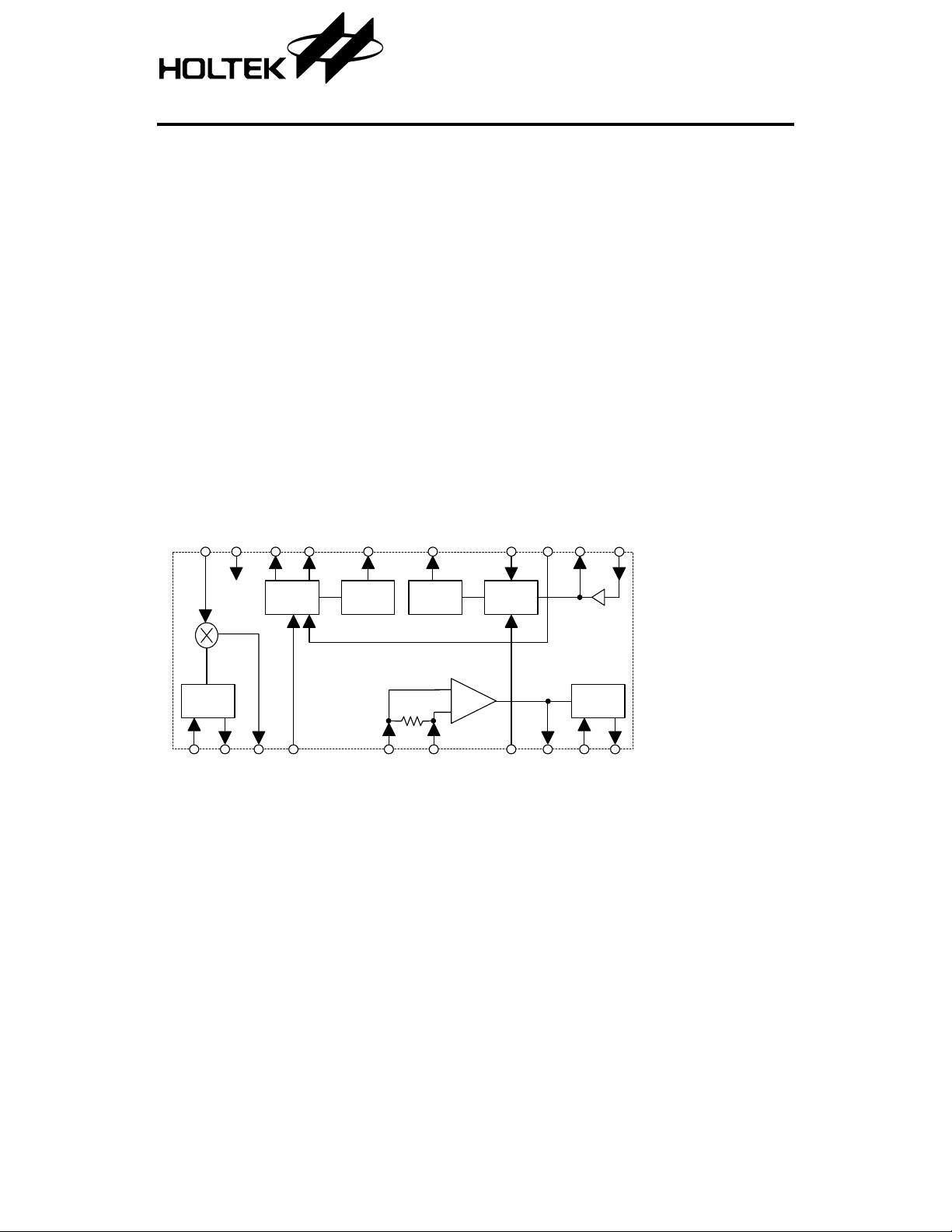
The HT9011 is designed for FM communication
system devices. It combines a paging system,
mixer, IF limiter, Quadrature detector, opera
tion amplifier, comparator and more. The
Block Diagram
MIXI
REGCGND REGO ALM FSKO CHG LPFOBS
=1.1V typ.
ALM
=1.1mA typ.
CCQ
FM IF Detector
Built-in low-pass filter and waveform shap
·
-
-
-
ing circuit enable the extraction of FSK sig
nals from voice signals
Built-in battery-saving function for longer
·
battery life time
High transmission rate: 1200 bps
·
20-pin SSOP package (0.65mm Pitch)
·
HT9011 could provide the customer¢s PAGER
system with total solution along with Holtek¢s
POCSAG Pager Controller series products.
LPFI
-
-
Mixer
OSC
OSCOOSCI MIXO
REG. ALARM
VCC FSKR
FSK
COM P.
IF IN
Quick
C harge
IF A m p
1 March 1, 2000
AM P
Q uad D et
AFOQUADIF ODEC

Pin Assignment
Preliminary
HT9011
OSCI
OSCO
MIXO
VCC
IF IN
DEC
FSKR
IF O
QUAD
AFO
1
2
3
4
5
6
7
8
9
10
MIXI
20
GND
19
REGO
18
REGC
17
ALM
16
FSKO
15
CHG
14
BS
13
LPFO
12
LPFI
11
H T 9011
2 0 S S O P
Pin Description
Pin No. Pin Name I/O Description
1 OSCI I
2 OSCO O
3 MIXO O
4 VCC
5 IFIN I Input terminal for IF Amp.
6 DEC I Bias Decoupling
7 FSKR I
8 IFO O
9 QUAD I
10 AFO O FM demodulator output pin
11 LPFI I Low Pass Filter Input pin
12 LPFO O Low Pass Filter Output pin
13 BS I
These pins are connected to the external parts of an oscillating
circuit.
Mixer output pin. Connect a 455kHz ceramic filter between this
pin and the IFIN pin.
Positive power supply
¾
Reference input of differential amplifier for waveform shaping.
Connect the capacitor externally.
IF Amplifier Output pin. Connect the discriminator through the coupling capacitor.
FM demodulator phase shift input pin connected to a quadrature
detector phase shifter.
Battery-saving Control pin
²H² Normal Operation
²L² Battery-saving
2 March 1, 2000

Preliminary
Pin No. Pin Name I/O Description
Control pin for quick charge-discharge circuit.
14 CHG I
15 FSKO O FSK NRZ data output
16 ALM O
17 REGC O
18 REGO O
19 GND
20 MIXI I MIXER Input terminal
²H² turn on quick charge-discharge
²L² turn off quick charge-discharge
Output pin for Low Voltage Alarm
@1.1V, this pin becomes ²H² (@VCC) and can indicate dete
At V
CC
rioration of battery.
Control pin of external transistor for regulator of external power
supply.
Externally connect the PNP transistor
Output voltage monitoring pin of regulator for external power
supply.
Negative power supply, ground
¾
HT9011
Absolute Maximum Ratings
Power Supply Voltage............VCC-0.3V to 4.0V Power Dissipation..................................730mW
Operating Temperature range ........0°Cto45°C
Storage Temperature.................-55°Cto150°C
-
Note: These are stress ratings only. Stresses exceeding the range specified under ²Absolute Maxi-
mum Ratings² may cause substantial damage to the device. Functional operation of this device
at other conditions beyond those listed in the specification is not implied and prolonged exposure to extreme conditions may affect device reliability.
3 March 1, 2000
 Loading...