

Features
•
Operating voltage: 5.0V
•
Long delay time
–
0.8 seconds (SEL=VSS, 256K DRAM)
–
0.2 seconds (SEL=VDD/open, 64K DRAM)
•
25kHz sampling rate
•
Continuous variable delay time
Applications
•
Mixers
•
Karaoke systems
General Description
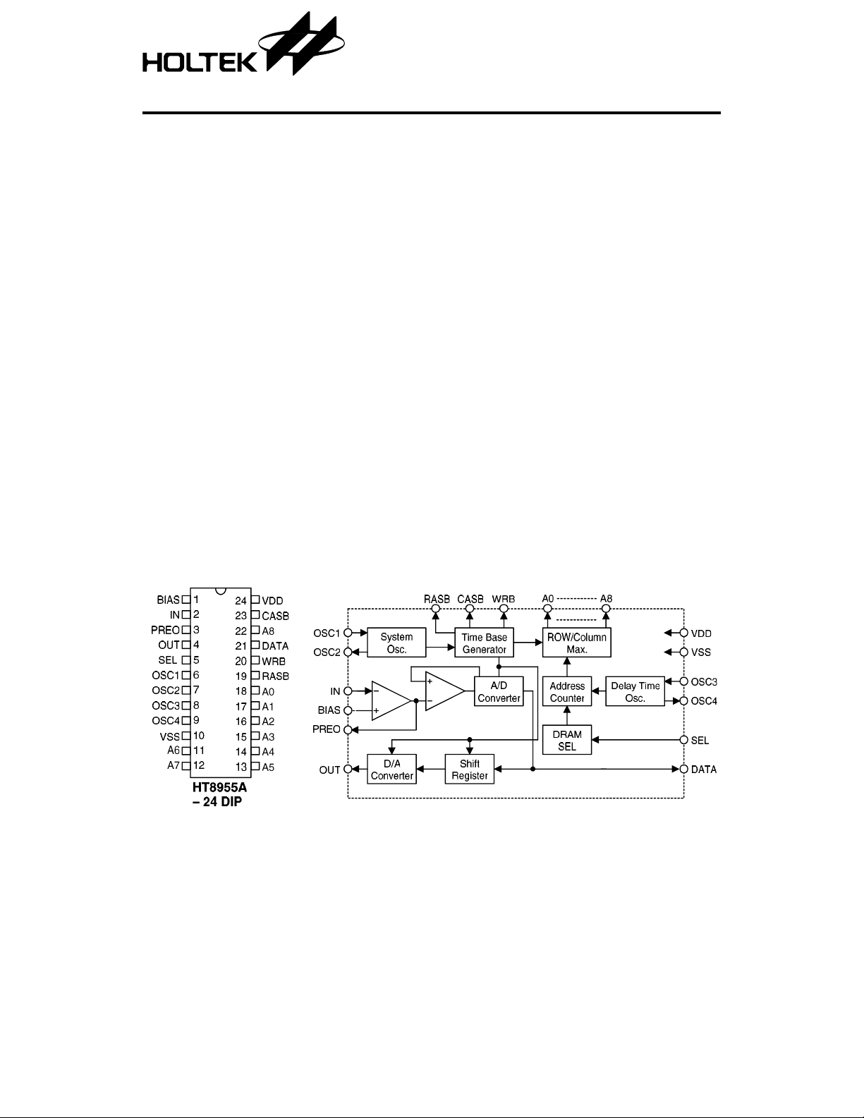
The HT8955A is a CMOS LSI digital audio
signal delay processor. It is designed for
audio system applications including echo
generators, karaoke systems, sound effect
generators, etc.
The chip consists of a built-in pre-amplifier,
on-chip oscillato r, DRAM interface, 10-bit A/D
and D/A converters as well as control logic. It
provides continuously adjustable delay time up
to 0.8/0.2 seconds at a s ampling rate of 25kHz
HT8955A
Voice Echo
•
Built-in pre-amplifier
•
Low distortion
•
High S/N ratio
•
Wide frequency response
•
PCM 10-bit A/D and D/A converters
•
24-pin DIP package
•
Echo generators
•
Sound effect generators
when combined with an external DRAM
(41256/4164). The HT8955A is superior to a
conventional BBD delay un it in its low distortion, high S/N ratio and long delay time. Its
sophisticated lo w pa ss filter wil l not e nd in the
normal application s due to the high sampling
rate (25~50kHz). Hence, the HT8955A is excellent for audio delay sys tem applications. It is
offered in a 24-pin dual-in-line package.
Pin Assignment Block Diagram
1 5th May ’98
HT8955A
Pad Coordinates Unit: µm
Pad
No.
1 –1138.00 796.50 14 1141.50 –547.00
2 –1141.00 523.50 15 1141.50 –197.50
3 –1136.50 201.50 16 1141.50 111.50
4 –1136.50 –163.00 17 1141.50 461.00
5 –1137.00 –507.00 18 1141.50 770.50
6 –1149.00 –774.00 19 896.00 811.00
7 –854.50 –853.50 20 645.00 810.50
8 –548.00 –831.50 21 435.00 794.00
9 –198.50 –831.50 21 335.00 794.00
10 111.50 –831.50 22 150.00 779.00
11 461.00 –831.50 23 –35.00 779.00
12 773.00 –831.50 25 –264.00 806.00
13 1122.50 –831.50
Chip size: 2170
* The IC substrate should be connected to VSS in the PCB layout artwork.
× 2200 (µm)
2
XY
Pad
Pin Description
Pin No. Pin Name I/O
1 BIAS O OP Non-inverted
2 IN I OP Inverted Audio signal input pin (inverted)
3 PREO O OP OUTPUT Pre-amplifier output pin
4 OUT O — Delayed audio signal output pin
5 SEL I Pull-High
6 OSC1 I — System oscillator input
7 OSC2 O — System oscillator output
8 OSC3 I — Delay time control oscillator input
9 OSC4 O — Delay time control oscillator output
10 VSS I — Negative power supply (GND)
11 A6 O CMOS OUT Connects to DRAM A6
12 A7 O CMOS OUT Connects to DRAM A7
Internal
Connection
Description
Internal pre-amplifier bias
Connects to a decoupling capacitor
DRAM type selection:
VDD or Open: 64Kb
VSS: 256Kb
No.
XY
2 5th May ’98
HT8955A
Pin No. Pin Name I/O
Internal
Connection
Description
13 A5 O CMOS OUT Connects to DRAM A5
14 A4 O CMOS OUT Connects to DRAM A4
15 A3 O CMOS OUT Connects to DRAM A3
16 A2 O CMOS OUT Connects to DRAM A2
17 A1 O CMOS OUT Connects to DRAM A1
18 A0 O CMOS OUT Connects to DRAM A0
19 RASB O CMOS OUT Connects to DRAM RASB
20 WRB O CMOS OUT Connects to DRAM WRB
21 DATA I/O CMOS I/O Data I/O pin
22 A8 O CMOS I/O Connects to DRAM A8
23 CASB O CMOS I/O Connects to DRAM CASB
24 VDD I — Positive power supply
Absolu te Maximum Ra tin g s*
Supply Voltage.................................–0.3V to 6V Storage T emperature.................–50°C to 125°C
Input Voltage................. V
–0.3V to VDD+0.3V Operating Temperature...............–20°C to 70°C
SS
*Note: These are stress ra tings on ly. Stresses exceeding the range spe cified un der “Abso lute Maxi-
mum Ratings” ma y cause substantial damage to the device. Functional operation of this
device at other conditions beyond those listed in the specification is not implied and prolonged
exposure to extreme condition s may affect device reliability.
Electrical Characteristics (Ta=25°C)
Symbol Parameter
V
DD
I
OP
A
V
A
V
V
IL
Operating Voltage — — 4.5 5.0 5.5 V
Operating Current 5V
Pre-amplifier Voltage Gain 5V
Comparator Voltage Gain 5V
“L” Input Voltage — — 0 — 0.3V
Test Conditions
V
DD
Conditions
No load,
f
=640kHz
OSC
>100kΩ
R
L
Open loop
>100kΩ
R
L
Open loop
3 5th May ’98
Min. Typ. Max. Unit
—2.58mA
—2000—V/V
—2000—V/V
V
DD

HT8955A
Symbol Parameter
V
IH
V
OMAX
“H” Input Voltage — — 0.7V
Maximum Output Voltage 5V RL>470kΩ 11.5—V
Td
Test Conditions
V
DD
5V
Maximum Delay Time
Td 5V
S/N Signal to Noise Ratio 5V
THD Total Harmonic Distortion 5V
Functional Description
The HT8955A is a single chip LSI with an external DRAM. It is designed for processing audi o
signal delay. The chip includes a built-in pre amplifier, 10-bit A/D and D/A converters. The
A/D and D/A converters ensure low distortion as
well as high S/N ratio of the audio delay system.
The chip also provides two sets of oscillation
circuit for system sampling rate and audio echo
delay time.
Conditions
Min. Typ. Max. Unit
—VDDV
DD
SEL=open, 25kHz
sampling rate
SEL=VSS, 25kHz
sampling rate
=1V, 400Hz
V
O
BW=10kHz
V
=1V, 400Hz
O
BW=7kHz
0.15 0.2 — s
0.6 0.8 — s
—55—dB
—0.5—%
demands an external resistor between the
OSC3 and OSC4 pins. By altering the oscillation resistor, its delay time can be continuously
adjusted up to 0.8/0.2 seconds at a 25kHz sampling rate for DRAM of 256Kb/64Kb.
Playing function block diagram
Syste m os c illator
The HT8955A provides two oscillators, one for
the sampling rate and one for echo delay time.
The sampling rate o scillato r requi res an exte rnal resistor between the OSC1 and OSC2 pins.
A higher sampling rate (25~50kHz) can thus be
derived by adjusting the oscillation resistor
without having a so phisticated low pass filter.
The delay time oscillator, on the other hand,
DRAM selectio n
The HT8955A can interface with a DRAM for
storing delay signals. T he type along with the
maximum delay time of DRAM is determined
by the status of the SEL pin as shown:
SEL Connection
DRAM
Type
Delay Time
VDD or Open 64Kb 0. 2 sec on ds
VSS 256Kb 0.8 seconds
4 5th May ’98

Application Circuits
Low cost echo
HT8955A
5 5th May ’98

Basic KARAOKE syste m
HT8955A
6 5th May ’98

Basic KARAOKE syste m with pre-emphasis
HT8955A
7 5th May ’98
 Loading...