Holtek Semiconductor Inc HT8950, HT8950A Datasheet

Features
•
Operating voltage: 2.4~4.0V
•
On-chip SRAM
•
Robot function
•
Vibrato function
•
8kHz sampling rate
•
7-step level shifting
Applications
•
Toys
•
Mixers
•
Recorders
General Description
The HT8950 is a single chip CMOS LSI voice
modulator. It provides 7 steps to shift the frequency of an input voice, producing a dramati cal change in the outp ut.
The HT8950 provides two special effects: Vibrato and Robot. The Vibrato effect is generated
by alternating the freq ue ncy o f an i nput signa l
up and down at a rate of 8Hz. The Robot function, on the other hand, converts an input voice
into a Robot voice. B oth effects can be se lected
depending on which pin is triggered, either
ROB or VIB. For the output frequency level
shifting, the chip provides 7 steps which can be
selected from the two groups of pins namely,
HT8950
Voice Modulator
•
8-bit A/D and D/A converters
•
LED indicator with voice level
•
Push button selection or electronic mode
•
Few external components required
•
16-pin/18-pin DIP package
•
Audio system
•
Speech system
•
Telephone system
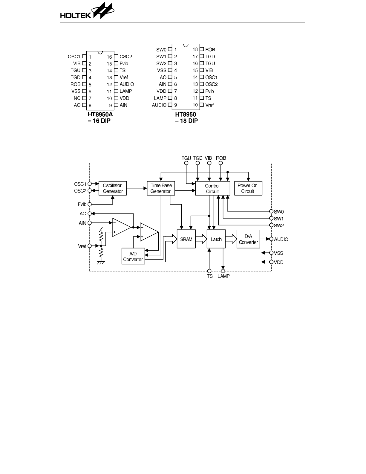
SW0, SW1 and SW2 for electronic direct selection and ROB, TGD, TGU and VIB for push
button selection.
The HT8950 includes a built-in microphone amplifier with an intern al bias, an 8-bit A /D converter, a built-in SRAM as well as a current
output type 8-bit D/A converter. The 8-bit A/D
and D/A converters with a sampling rate of
8kHz ensures a high quality and high S/N ratio
output voice. The chip provides an LED indicator which flashes with the vo lume of the input
voices. It is offered in a 16-pin or 18-pin DIP
package.
1 5th May ’98

Pin Assignment
Block Diagram
HT8950
2 5th May ’98

HT8950
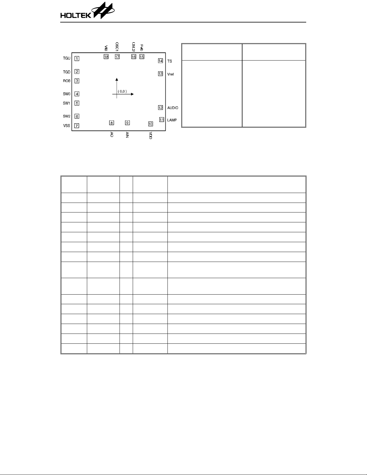
Pad Coordinates Unit: µm
Pad
No.
Chip size: 2350
∗ The IC substrate should be connected to VSS in the PCB layout artwork.
× 2080 (µm)
2
XY
1 –957.0 720.5 10 732.0 –774.0
2 –957.0 423.5 11 984.0 –675.0
3 –957.0 210.0 12 956.5 –400.0
4 –957.0 –87.0 13 956.5 374.5
5 –957.0 –299.5 14 956.5 671.5
6 –957.0 –596.5 15 530.5 765.5
7 –962.0 –815.0 16 345.50 765.5
8 –161.5 –747.5 17 –33.50 765.5
9 200.5 –747.5 18 –287.50 765.5
Pad
No.
Pin Description (18 Pin Version)
Pin No. Pin Name I/O
1 SW0 I Pull-High Function setting pin (for electronic setting)
2 SW1 I Pull-High Function setting pin (for electronic setting)
3 SW2 I Pull-High Function setting pin (for electronic setting)
4 VSS I — Negative power supply (GND)
5 AO O — Internal amplifier output
6 AIN I — Internal amplifier input (inverted)
7 VDD O — Positive power supply
8LAMPO
9
10 Vref I — Internal amplifier reference voltage
11 TS I — For IC test only
12 Fvib O — Vibrato frequency control
13 OSC2 O — Oscillator output
14 OSC1 I — Oscillator input
15 VIB I Pull-High Switch to Vibrato mode (toggle)
AUDIO O
Internal
Connection
NMOS
Open Drain
PMOS
Open Drain
Description
Lamp output (brightness changes with voice volume)
Audio output
XY
3 5th May ’98

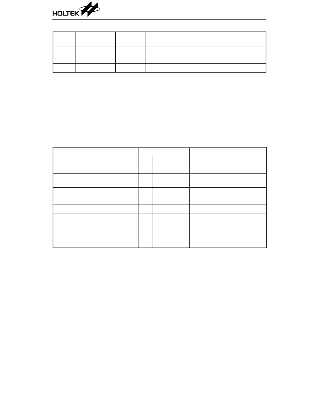
HT8950
Pin No. Pin Name I/O
Internal
Connection
Description
16 TGU I Pull-High Switch to Upward step mode
17 TGD I Pull-High Switch to Downward step mode (internal pull-high)
18 ROB I Pull-High Switch to Robot mode (internal pull-high)
Absolu te Maxim u m Rating s*
Supply Voltage.................................–0.3V to 6V Storage Temperature.................–50°C to 125°C
Input Voltage................. V
–0.3V to VDD+0.3V Operating Temperature...............–20°C to 70°C
SS
*Note: These are stress ra tings on ly. Stresses exceeding th e range spe cified und er “Absolute M axi-
mum Ratings” ma y cause substantial damage to the device. Functional operation of this
device at other conditions beyond those listed in the specification is not implied and prolonged
exposure to extreme condition s may affect device reliability.
Electrical Characteristics (Ta=25°C)
Symbol Parameter
V
I
OP
V
I
LAMP
A
I
O
V
V
f
OSC
Operating Voltage — — 2.4 3.0 4.0 V
DD
Operating Current 3V
Input Signal 3V — — — 580 mV
IN
Lamp Sink Current 3V VOL=1.3V 5.0 9.5 — mA
OPA Gain Value 3V Open loop — 2000 —
V
Audio Output Voltage 3V During silence — –1.0 — mA
“H” Input Voltage — — 0.7V
IH
“L” Input Voltage — — — — 0.3V
IL
Oscillating Freque ncy 3V R
Test Conditions
V
DD
Conditions
No load,
f
=640kHz
OSC
=47kΩ — 512 — kHz
OSC
Min. Typ. Max. Unit
— 2.0 10 mA
——V
DD
V
DD
4 5th May ’98
 Loading...