

Features
Operating voltage: 2.4V~5.0V
·
Driver speaker (32W)VDD=4.5V,
·
I
=90mA
DD
Programmable tone melody generator
·
ADPCM, m-law PCM, PCM synthesis
·
Wide range of sampling rate for voice
·
synthesis
Minimum sampling rate step: 100Hz
·
Voice melody mixed output
·
Programmable 2 channels of melody
·
mixed output
Programmable 2 channels of voice
·
mixed output
General Description
The HT85XXX family is a series of programma
ble speech synthesizers and tone generators de
signed for user-defined voice and melody
applications. It provides various sampling
rates and beats, tone levels, tempos for the
speech synthesizer and melody generator.
The HT85XXX series has a built-inhigh quality,
currenttypeD/Aoutputswith 16levelsof volume
control. The user¢s commands enable the user to
HT85XXX
Green Voice
13 kinds of melody beats
·
5 octaves of tone level and 18 tempos
·
16 levels of digital volume control
·
Eight programmable I/O pins
·
Four programmable input pins
·
Provides 36 sec to 96 sec of voice capacity
·
Timer controller
·
Voice fill-in function
·
Powerful user-defined functions
·
Power-on initial setting
·
28-pin SKDIP package
·
program the powerful custom functionsuch as to
build-in a tiny controller. The Green Voice pro
vides various operational functions similar to
arithmetic operation, logic operation, branch de
cision, random counter, and a programmable
timer. The Green Voice series are suitable for
versatilevoiceandsoundeffect applications.
The HT85XXX Green Voice series is Easy For-
TM
mat
supported.
TM
-
-
Selection Table
The HT85XXX series provides various voice capacity as shown below:
Part No. HT85036 HT85048 HT85072 HT85096
ROM 768Kb 1024Kb 1536Kb 2048Kb
Voice
Length
Note: The voice capacity is based on a sampling rate of 4-bit ADPCM 5.25kHz.
*: under development.
Green VoiceTMand Easy FormatTMare trademark of Grow With Me, Inc.
36 sec 48 sec 72 sec 96 sec
1 August 24, 2000
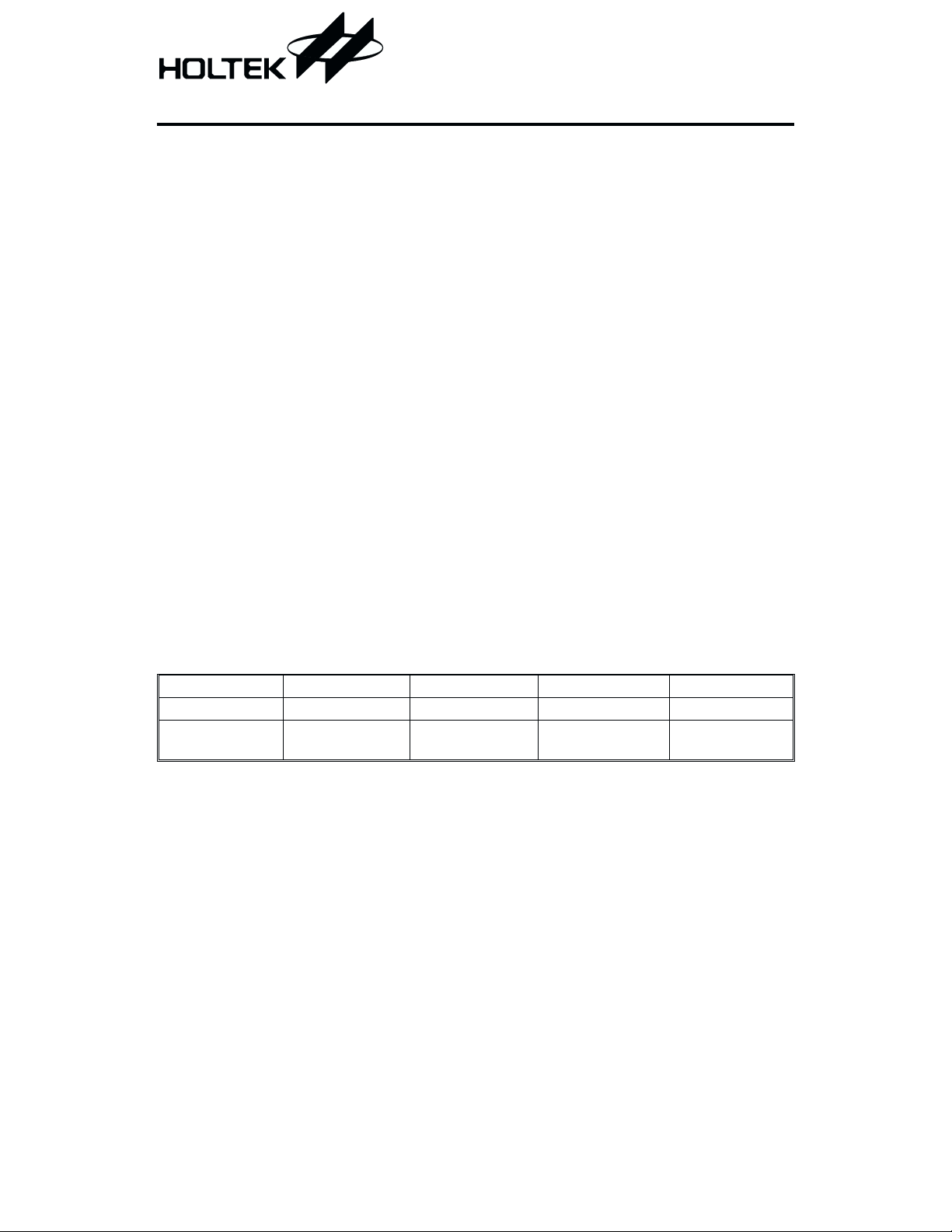
Block Diagram
HT85XXX
OSC
PB0~PB7
PA0~PA3
VDD
VSS
Tim e Base
G enerator
D ecoder
C ontroller
Pin Assignment
NC
1
NC
2
PP0
3
PDA
4
PP1
5
VDD
6
AUD
7
NC
8
PB7
9
PB6
10
PB5
11
PB4
12
PB3
13
PB2
14
H T 8 5 X X X
28 S K D IP
and
28
27
26
25
24
23
22
21
20
19
18
17
16
15
NC
NC
NC
NC
NC
OSC
VSS
VSS
PA0
PA1
PA2
PA3
PB0
PB1
Tone/M elody
Generator
DATA
and
User
Instruction
ROM
D/A
and
G reen
Driver
Speech
Synthesizer
AUD
PDA
PP1
PP0
2 August 24, 2000
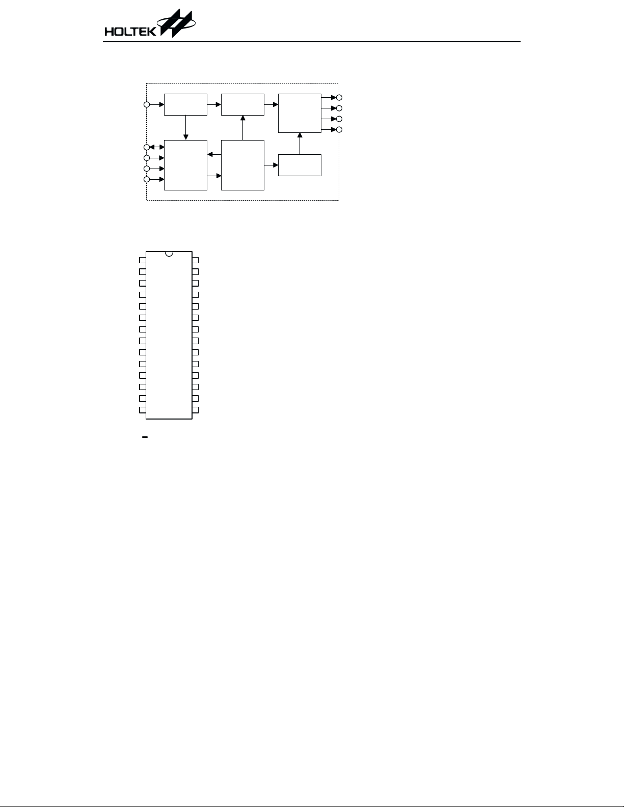
Pad Assignment
HT85036, HT85048, HT85072, HT85096
PP0
PDA
PP1
VDD
VDD
AUD
1
2
3
4
5
6
(0 ,0 )
21
20
19
18
HT85XXX
OSC
VSS
VSS
PA0
13
7 8 9 10 11
PB5
PB6
PB7
12
PB2
PB3
PB4
Chip size: 2315 ´ 2875 (mm)
15 16
14
PA3
PB0
PB1
2
* The IC substrate should be connected to VSS in the PCB layout artwork.
Pad Coordinates
HT85036, HT85048, HT85072, HT85096
Pad No. X Y Pad No. X Y
1
2
3
4
5
6
7
8
9
10
-785.05 -216.50
-785.05 -377.10
-785.05 -533.85
-785.05 -671.55
-970.35 -761.05
-973.35 -910.10
-577.70 -1172.50
-443.35 -1172.50
-226.85 -1172.50
-132.35 -1172.50
11 44.15
-1172.50
12 178.65
13 355.15
14 489.95
15 662.95
16 789.70
17 962.20
18 961.30
19 958.10
20 956.30
21 960.96
3 August 24, 2000
17
PA1
PA2
Unit: mm
-1172.50
-1172.50
-1172.50
-1172.50
-1172.50
-1172.50
-861.10
-634.65
-505.15
-192.93
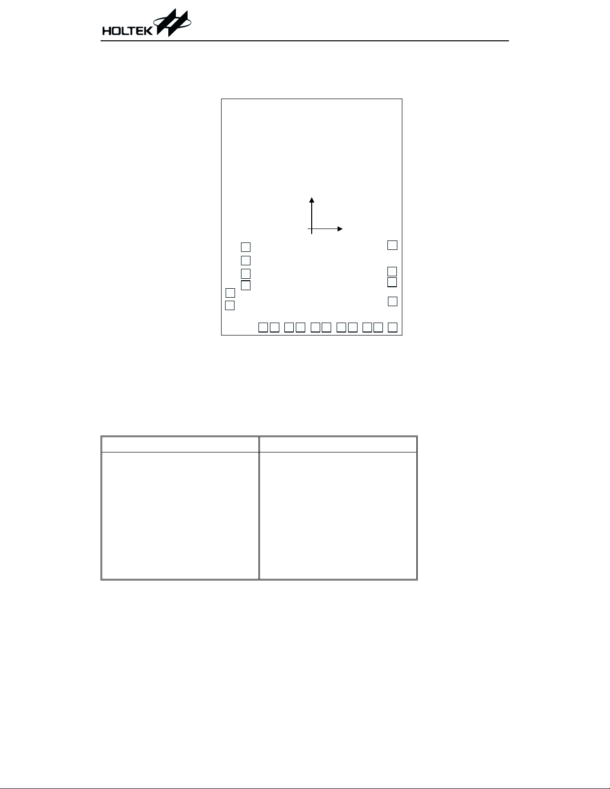
Pin Description
HT85XXX
Pin No. Pin Name I/O
1, 2, 8,
24~28
3, 4, 5
NC
PP0, PDA,
PP1
6 VDD
7 AUD O
15~9 PB1~PB7 I/O
16 PB0 I/O
20~17 PA0~PA3 I
21, 22 VSS
23 OSC I
Internal
Connection
¾¾
O
¾
¾¾
PMOS
Open Drain
Pull-high
or CMOS
Pull-high
or CMOS
Wake-up
Pull-high
¾¾
¾
No connection
Green Voice Speaker control pin
Positive power supply
Audio output for driving an external transistor
Bidirectional I/O pins
Can be optioned as trigger inputs or LED outputs
Bidirectional I/O pins
Can be optioned as CDS interface with internal
Schmitt trigger input
Trigger inputs
Can also be configured as wake-up inputs
Negative power supply, ground
Built-in RC oscillator
An oscillator resistor is connected between OSC and VSS
Absolute Maximum Ratings
Supply Voltage .................................-0.3V to 6V
Input Voltage .................V
-0.3V to VDD+0.3V
SS
Description
Storage Temperature.................-50°Cto125°C
Operating Temperature ..............-20°Cto70°C
Note: These are stress ratings only. Stresses exceeding the range specified under ²Absolute Maxi-
mum Ratings² may cause substantial damage to the device. Functional operation of this device
at other conditions beyond those listed in the specification is not implied and prolonged exposure to extreme conditions may affect device reliability.
Electrical Characteristics
Symbol Parameter
V
I
I
I
I
f
DD
STB
DD
OL
O
SYS
Operating Voltage
Standby Current 3V No load, system HALT
Operating Current 3V
PB0~PB7 Sink Current 3V
Max. AUD Output Current 3V
System Frequency 3V
Test Conditions
V
DD
Conditions
¾¾
No load, f
V
=0.3V
OL
V
=0.6V
OH
=240kW
R
OSC
4 August 24, 2000
SYS
=4MHz
Min. Typ. Max. Unit
2.4
¾
¾
¾
13
58mA
46
-1.5 -2 ¾
3.6 4.0 4.4 MHz
Ta=25°C
5.2 V
mA
mA
¾
mA

Functional Description
The Green Voice series is a series of program
mable speech synthesizers and melody genera
tors. It provides various sampling rates and
beats, tone levels, tempos for speech synthe
sizer and melody generator. For voice synthe
sizer, the Green Voice provides 8-bit PCM, 6-bit
m-law PCM and 4-bit ADPCM synthesis. In
HT85XXX series, a mixed output of two chan
nels PCM synthesis is allowed but only one
channel ADPCM synthesis is allowed. For mel
ody generator, the Green Voice supports a tone
melody and PCM melody generator and two
channels mixed output for the whole series.
The Green Voice series build-in 8 programma
ble I/O pins and 4 programmable input pins
along with powerful user¢s command. The
user¢s instructions are employed to develop
new and customized functions for a wide vari
ety of innovative applications.
Speech and melody analysis
The speech and melody sources of the Green
Voice can be recorded and edited from the PC
sound card and media tools. Holtek¢s CAD tools
first load a speech source file as .WAV or .PCM
format, then transfer the speech file as PCM,
LOG-PCM or ADPCM format, and finally save
it to the internal mask ROM by changing a
layer of the mask. The PCM format generates a
higher sound quality whereas the ADPCM format brings about a longer recording capacity.
The melody source can either be in the .MID or
in the .MLD format.
The .MID file is the standard format of the win
dows media tools. The .MLD file is a text for
mat. After the .MID file is compiled, the .MLD
file is automatically generated.
The Green Voice can support the following com
pression format of the voice .WAV and .PCM
file: AD4, PCM8, m-law PCM.
Current type D/A output
-
The HT85XXX series supply high accuracy cur
rent type D/Aoutput pins for audio output. The
output volume is changeable from 0 to 15 digi
tal levels by writing a value to the VOLUME
registers. The D/A pins are PMOS open drain
structure and ouput synthesized signals for
driving a speaker through an external NPN
transistor when the chip is active. However, it
becomes floating when the chip is in the
standby state. An 8050 type transistor with
h
=150 is recommended for the output driver
FE
of the D/A output pin.
-
Melody/Tone generator
The HT85XXX family has a built-in mel
ody/tone generator. The generator can generate
13 different kinds of melody beats, 5 octaves of
tone level, 18 tempos, and 2 channels mixed
output. Of these components, the melody tempo
is changeable and generates sound effects by
writing a control value to the TEMPO register.
The chip provides the following 18 tempos, 13
beats, and 5 octaves for user¢s programming.
·
18 tempos (Beats/Min.)
68 78 82 93 100 105
109 114 119 125 132 139
147 156 179 192 227 310
·
13 beats
1241121816141312233
, ,,, ,,,, ,,,,
-
·
-
5 octaves
C1~B1, C2~B2, C3~B3, C4~B4, C5~B5
433
1
4
2
-
HT85XXX
-
-
-
2
5 August 24, 2000

PCM/ADPCM synthesizer
The HT85XXX family contains a PCM and
ADPCM synthesizer. The synthesizer offers a
wide range of sampling rates from 4kHz to
24kHz for PCM synthesis and 4kHz to 16kHz
for ADPCM synthesis. The sampling rate of the
synthesizer can be changed by writing a control
value to the sampling rate register. It also sup
ports a small variety of 100Hz. For a higher
performance sound quality, the PCM coding is
required. But for a longer recording capacity,
the ADPCM coding is recommended.
The capability of the voice sampling rate for
various voice compression format.
f
OSC
PCM8
m-law
PCM
AD4
4M 12kHz 11kHz 8kHz
5M 15kHz 14kHz 10kHz
6M 18kHz 16kHz 12kHz
8M 24kHz 22kHz 16kHz
Oscillator configuration
The HT85XXX series provides an RC oscillator
for the system clock. The system oscillator
stops in the standby state so as to reduce power
consumption.
For the oscillator circuit, an external resistor is
required between OSC and VSS. The oscillator
frequency is typically 4MHz for an external re
sistor of 240kW. The RC type of oscillator offers
the most cost-effective solution, although the
frequency of the oscillation may vary with tem
perature and the chip itself due to process vari
ation.
R
OSC
f
OSC
4M
5M
6M
8M
HT84EVA HT84P00 IC
180kW 240kW 240kW
150kW 210kW 210kW
120kW 180kW 180kW
91kW 150kW 150kW
Mask options
The following options have to be defined to en
sure a proper system functioning:
·
Pull-high resistor: 33kW/98kW (3V)
·
Key debounce time:0ms~255ms (f
HT85XXX
=4MHz)
OSC
-
-
-
-
6 August 24, 2000

Application Circuits
Basic application
HT85XXX
EASY 4
V
DD
VDD
1mF
8050
1mF
8050
PP0
PP1
PDA
AUD
OSC
R
OSC
VSS
EASY 8
V
DD
VDD
PP0
PP1
PDA
AUD
OSC
R
OSC
VSS
PA0
PA1
PA2
PA3
PB7
PB6
PB5
PB4
PB3
PB2
PB1
PB0
PA0
PA1
PA2
PA3
PB7
PB6
PB5
PB4
PB3
PB2
PB1
PB0
TR1
TR2
TR3
TR4
OUT8
OUT7
OUT6
OUT5
OUT4
OUT3
OUT2
OUT1
TR1
TR2
TR3
TR4
OUT6
OUT5
OUT4
OUT3
OUT2
OUT1
TR5
TR6
TR7
TR8
1mF
8050
1mF
8050
V
DD
R
V
DD
R
EASY 4-1
VDD
PP0
PP1
PDA
AUD
OSC
OSC
VSS
EASY 12
VDD
PP0
PP1
PDA
AUD
OSC
OSC
VSS
PA0
PA1
PA2
PA3
PB7
PB6
PB5
PB4
PB3
PB2
PB1
PB0
PA0
PA1
PA2
PA3
PB7
PB6
PB5
PB4
PB3
PB2
PB1
PB0
TR1
TR2
TR3
TR4
OUT7
OUT6
OUT5
OUT4
OUT3
OUT2
OUT1
TR1
TR2
TR3
TR4
OUT5
OUT4
OUT3
OUT2
OUT1
TR5
TR6
TR7
TR8
TR9
TR10
TR11
TR12
7 August 24, 2000

HT85XXX
1mF
EASY 16
V
DD
VDD
PP0
PP1
PDA
8050
1mF
8050
R
V
DD
R
AUD
OSC
OSC
VSS
EASY 20
VDD
PP0
PP1
PDA
AUD
OSC
OSC
VSS
PA0
PA1
PA2
PA3
PB7
PB6
PB5
PB4
PB3
PB2
PB1
PB0
PA0
PA1
PA2
PA3
PB7
PB6
PB5
PB4
PB3
PB2
PB1
PB0
TR1
TR2
TR3
TR4
OUT4
OUT3
OUT2
OUT1
TR1
TR2
TR3
TR4
OUT3
OUT2
OUT1
TR5
TR6
TR7
TR8
TR5
TR6
TR7
TR8
TR9
TR10
TR11
TR12
TR9
TR10
TR11
TR12
TR13
TR14
TR15
TR16
TR13
TR14
TR15
TR16
TR17
TR18
TR19
TR20
8 August 24, 2000

HT85XXX
EASY 24
V
DD
VDD
1mF
8050
PP0
PP1
PDA
AUD
OSC
R
OSC
VSS
PA0
PA1
PA2
PA3
PB7
PB6
PB5
PB4
PB3
PB2
PB1
PB0
TR1
TR2
TR3
TR4
OUT2
OUT1
TR5
TR6
TR7
TR8
TR9
TR10
TR11
TR12
TR13
TR14
TR15
TR16
TR17
TR18
TR19
TR20
TR21
TR22
TR23
TR24
EASY 28
V
DD
VDD
1mF
8050
PP0
PP1
PDA
AUD
OSC
R
OSC
VSS
PA0
PA1
PA2
PA3
PB7
PB6
PB5
PB4
PB3
PB2
PB1
PB0
TR1
TR2
TR3
TR4
OUT1
TR5
TR6
TR7
TR8
TR9
TR10
TR11
TR12
TR13
TR14
TR15
TR16
TR17
TR18
TR19
TR20
TR21
TR22
TR23
TR24
TR25
TR26
TR27
TR28
9 August 24, 2000

HT85XXX
EASY 32
V
DD
VDD
1mF
8050
PP0
PP1
PDA
AUD
OSC
R
OSC
VSS
PA0
PA1
PA2
PA3
PB7
PB6
PB5
PB4
PB3
PB2
PB1
PB0
TR1
TR2
TR3
TR4
TR5
TR6
TR7
TR8
TR9
TR10
TR11
TR12
TR13
TR14
TR15
TR16
TR17
TR18
TR19
TR20
TR21
TR22
TR23
TR24
TR25
TR26
TR27
TR28
TR29
TR30
TR31
TR32
EASY 64
V
DD
VDD
1mF
8050
PP0
PP1
PDA
AUD
OSC
R
OSC
VSS
PA3
PA2
PA1
PA0
TR1
TR9
PB6
TR17
PB5
TR25 TR 26 TR27 TR 28 TR 29 TR30 TR 31
PB4
TR33 TR 34 TR35 TR 36 TR 37 TR38 TR 39
PB3
TR41 TR42 TR43 TR 44 TR45 TR 46 TR47
PB2
TR49 TR50 TR51 TR 52 TR53 TR 54 TR55
PB1
TR57 TR58 TR59 TR 60 TR61 TR 62 TR63
PB0
TR2
TR10
TR18 TR 19 TR 20 TR 21 TR 22 TR23
TR3
TR11
TR4
TR12
TR5
TR13
TR6
TR14 TR 15
TR7
TR8
TR16
TR24
TR32
TR40
TR48
TR56
TR64
PB7
Note: In Easy 64 mode, only falling edge trigger can be used in input state
In Easy 64 mode, the path command ²TRn?L:pathname² and ²TRn?H:pathname² are invalid
10 August 24, 2000

HT85XXX
Holtek Semiconductor Inc. (Headquarters)
No.3 Creation Rd. II, Science-based Industrial Park, Hsinchu, Taiwan, R.O.C.
Tel: 886-3-563-1999
Fax: 886-3-563-1189
Holtek Semiconductor Inc. (Taipei Office)
5F, No.576, Sec.7 Chung Hsiao E. Rd., Taipei, Taiwan, R.O.C.
Tel: 886-2-2782-9635
Fax: 886-2-2782-9636
Fax: 886-2-2782-7128 (International sales hotline)
Holtek Semiconductor (Hong Kong) Ltd.
RM.711, Tower 2, Cheung Sha Wan Plaza, 833 Cheung Sha Wan Rd., Kowloon, Hong Kong
Tel: 852-2-745-8288
Fax: 852-2-742-8657
Copyright Ó 2000 by HOLTEK SEMICONDUCTOR INC.
The information appearing in this Data Sheet is believed to be accurate at the time of publication. However, Holtek
assumes no responsibility arising from the use of the specifications described. The applications mentioned herein are
used solely for the purpose of illustration and Holtek makes no warranty or representation that such applications
will be suitable without further modification, nor recommends the use of its products for application that may pres
ent a risk to human life due to malfunction or otherwise. Holtek reserves the right to alter its products without prior
notification. For the most up-to-date information, please visit our web site at http://www.holtek.com.tw.
11 August 24, 2000
-
 Loading...