

HT82V731
Preliminary
Features
CMOS technology
·
Low power consumption
·
Two voltage output channel in the same
·
chip
Applications
Digital audio equipment
·
CD ROM/VCD
·
General Description
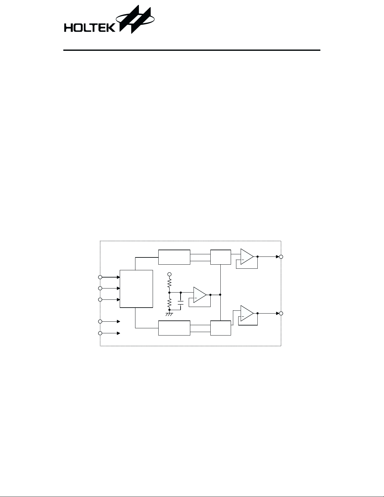
HT82V731 is a 16-bit digital-to-analog con
verter IC utilizing CMOS technology specially
designed for stereo audio application.
HT82V731 converts the 16 bits serial data into
an analog output voltage. The digital data is in
ternally converted to floating point expression
whose format consists of 10 bits mantissa and
7step exponent.
Audio D/A Converter
16-bit dynamic range
·
Low total harmonic distortion
·
5 voltage single power supply
·
8-pin SOP package
·
MPEG card
·
Using an R-string voltage divider, this floating
point expression data is then converted to
analog voltage.
It is compatible with TDA1311. It is available in
8-pin SOP package.
-
Block Diagram
BCK
WS
DIN
VDD
VSS
D ata Latch
Floating D ata
C onversion
V
DD
Floating D ata
C onversion
Out
+
DAC
Out
+
op
DAC
1 February 1, 2000
op
Out
+
op
RCH
LC H
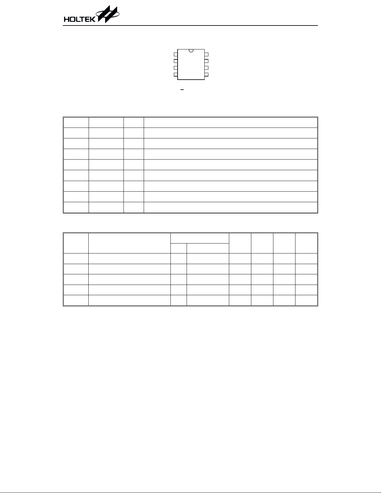
Pin Assignment
Preliminary
HT82V731
BCK
WS
DIN
VSS
1
2
3
4
RCH
8
NC
7
LC H
6
VDD
5
HT82V731
8 S O P
Pin Description
Pin No. Pin Name I/O Description
1
2
3
4
5
6
7
8
BCK
WS
DIN
VSS
VDD
LCH
NC
RCH
I Bit serial clock input
I Word select input
I Data input
Negative power supply
¾
Positive power supply
¾
O Left channel output
No connection
¾
O Right channel output
Electrical Characteristics
Ta=25°C
Symbol Parameter
Test Conditions
DD
Conditions
¾¾
V
V
O
Maximum Output Amplitude 5V
THD Total Harmonic Distortion 5V 1kHz, 0dB
DR Dynamic Range 5V
¾¾16¾
S/N Signal to Noise Ratio 5V 1kHz, 0dB
CT Cross Talk 5V 1kHz, 0dB
2 February 1, 2000
Min. Typ. Max. Unit
¾
2.5
0.12
¾
¾
Vpp
%
Bit
¾
82
¾
¾¾¾
dB
dB

Timing Diagrams
WS
t
r
t
t
f
h
BCK
Preliminary
HT82V731
DIN
Data
BCK
WS
LSBLSB+1 M SB M SB-1
MSB
LEFT
Sam ple O ut
Application Circuits
10
V
DD
W
+
1
2
3
+
47mF
BCK
HT82V731
WS
DATA
100nF
VSS
VDD
4
5
LSB
RCH
NC
LC H
LSB
MSB
RIGHT
420pF
22k
W
22k
22k
W
W
8
2.2nF
7
420pF
22k
6
W
2.2nF
+
100pF
+
100pF
3 February 1, 2000

Preliminary
HT82V731
Holtek Semiconductor Inc. (Headquarters)
No.3 Creation Rd. II, Science-based Industrial Park, Hsinchu, Taiwan, R.O.C.
Tel: 886-3-563-1999
Fax: 886-3-563-1189
Holtek Semiconductor Inc. (Taipei Office)
5F, No.576, Sec.7 Chung Hsiao E. Rd., Taipei, Taiwan, R.O.C.
Tel: 886-2-2782-9635
Fax: 886-2-2782-9636
Fax: 886-2-2782-7128 (International sales hotline)
Holtek Semiconductor (Hong Kong) Ltd.
RM.711, Tower 2, Cheung Sha Wan Plaza, 833 Cheung Sha Wan Rd., Kowloon, Hong Kong
Tel: 852-2-745-8288
Fax: 852-2-742-8657
Copyright Ó 2000 by HOLTEK SEMICONDUCTOR INC.
The information appearing in this Data Sheet is believed to be accurate at the time of publication. However, Holtek
assumes no responsibility arising from the use of the specifications described. The applications mentioned herein are
used solely for the purpose of illustration and Holtek makes no warranty or representation that such applications
will be suitable without further modification, nor recommends the use of its products for application that may pres
ent a risk to human life due to malfunction or otherwise. Holtek reserves the right to alter its products without prior
notification. For the most up-to-date information, please visit our web site at http://www.holtek.com.tw.
4 February 1, 2000
-
 Loading...