

14-Bit CCD/CIS Analog Signal Processor
Features
Low power CMOS : 350 mW
·
9 ADC clock latency for digital data output
·
14-bit 6 MSPS A/D converter
·
3-channel correlated double sampler
·
1~6 programmable gain
·
Input clamp circuitry for CDS-mode
·
Internal/external circuitfor CIS
·
General Description
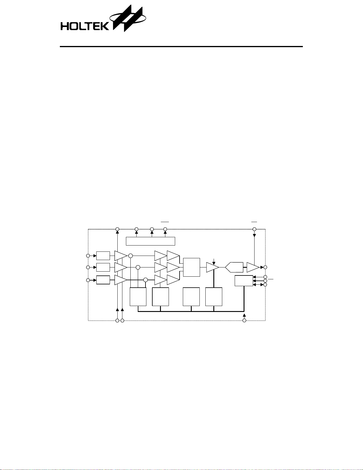
The HT82V14 is a complete analog signal pro
cessor for CCD imaging applications. It fea
tures a 3-channel architecture designed to
sample and condition the outputs of the
trilinear color CCD arrays. Each channel con
sists of an input clamp, Correlated Double
Sampler (CDS), offset DAC and Programmable
Gain Amplifier (PGA), multiplexed to a high
performance 14-bit A/D converter.
HT82V14
Internal/external voltage reference
·
Internal MUX for channel operation
·
1 or 3-channel operation
·
Pixel-rate or line-rate switch operation
·
Programmable 3-wire serial interface
·
+5V digital I/O compatibility
·
28-pin SOP/SOJ package
·
The CDS amplifiers may be disabled for use
with sensors such as Contact Image Sensors
(CIS) and CMOS active pixel sensors, which do
not require CDS.
The 14-bit digital output is multiplexed into an
8-bit output word that is accessed using two
read cycles. The internal registers are pro
grammed through a 3-wire serial interface,
which provides gain, offset, and operating mode
adjustments.
-
Block Diagram
RIN
GIN
BIN
CLP
CLP
CLP
CDSCLK1 CDSCLK2
O F F S E T R E F T C M L R E F
Voltage R eference
CDS
CDS
CDS
+
+
3´8 bits
DAC
Offset
+
VGA
VGA
VGA
3´2 bits
C oarse
Gain
OE
Pixel Rate
G uarantee
MUX
C onfig
R egister
1 July 12, 2000
PGA
3´5 bits
F in e
Gain
14-bit
ADC
ADC CLK
C ontrol
Port
D 13~D 0
SCLK
CS
SDATA
Pin Assignment
HT82V14
CDSCLK1
CDSCLK2
ADC CLK
OE
DRVDD
DRVSS
D 13/D 5
D 12/D 4
D 11/D 3
D 10/D 2
D9/D1
D8/D0
D7
D6
1
2
3
4
5
6
7
8
9
10
11
12
13
14
28
27
26
25
24
23
22
21
20
19
18
17
16
15
AVDD
AVSS
RIN
OFFSET
GIN
CML
BIN
REFT
REF
AVSS
AVDD
SLO AD
SCLK
SDATA
HT82V14
2 8 S O P /S O J
Pin Description
Pin No. Pin Name I/O Description
1 CDSCLK1 DI CDS reset clock pulse input
2 CDSCLK2 DI CDS data clock pulse input
3 ADCCLK DI A/D sample clock input for 3-channels mode
4OE
5 DRVDD
6 DRVSS
14~7 D0~D13 DO Digital data output
15 SDATA DIO Serial data input/output
16 SCLK DI Clock input for serial interface
17 CS
18, 27 AVSS
19, 28 AVDD
20 REF
21 REFT AO Reference decoupling
22 BIN AI Analog Input, blue
23 CML AO Internal reference output
24 GIN AI Analog Input, green
25 OFFSET AO CIS reference decoupling
26 RIN AI Analog input, red
DI Output enable
¾
¾
Digital driver power
Digital driver ground
DI Chip select
¾
¾
Analog ground
+5V analog supply
AO Reference decoupling
2 July 12, 2000
Absolute Maximum Ratings
HT82V14
Supply Voltage .............................-0.3V to 5.5V
Input Voltage ................V
-0.3V to VDD+0.3V
SS
Storage Temperature ......................0°Cto70°C
Operating Temperature ...............25°Cto50°C
Note: These are stress ratings only. Stresses exceeding the range specified under ²Absolute Maxi
mum Ratings² may cause substantial damage to the device. Functional operation of this device
at other conditions beyond those listed in the specification is not implied and prolonged expo
sure to extreme conditions may affect device reliability.
Electrical Characteristics
Symbol Parameter
Conversion Rate
3-channel Mode with CDS
1-channel Mode with CDS
A/D Converter
Resolution
Integral Nonlinearity
(INL)
Differential Nonlinearity
(DNL)
Analog Inputs
Full-scale Input Range
Input Limits
Input Capacitance
Input Current
Amplifiers
Coarse Gain Range
Coarse Gain Resolution
PGA Gain Range
PGA Gain Resolution
Offset Range
Offset Resolution
Test Conditions
Min. Typ. Max. Unit
V
5V±10% ¾¾¾
5V±10% ¾¾¾
DD
Conditions
6 MSPS
5 MSPS
5V±10% ¾¾14¾
5V±10% ¾¾±4.5 ¾
5V±10% ¾-0.5 ¾
1.2 LSB
5V±10% ¾¾4¾
TBD
TBD
¾
AV
DD
¾
¾mA
3 V/V
5V±10% ¾ AV
-0.3 ¾
DD
5V±10% ¾¾
5V±10% ¾¾
5V±10% ¾
1
5V±10% ¾¾2¾
5V±10% ¾
1
¾
2 V/V
5V±10% ¾¾5¾
5V±10% ¾-200 ¾
200 mV
5V±10% ¾¾8¾
+0.3
BIT
LSB
Vp-p
V
pF
Bits
Bits
Bits
-
-
3 July 12, 2000
HT82V14
Symbol Parameter
Power Supplies
AVDD
DRVDD
Power Consumption
Power Consumption
Digital Specifications
Symbol Parameter
Logic Inputs
V
IH
V
IL
I
IH
I
IL
C
IN
High Level Input Voltage 3.3V~5V
Low Level Input Voltage 3.3V~5V
High Level Input Current 3.3V~5V
Low Level Input Current 3.3V~5V
Input Capacitance 3.3V~5V
Logic Outputs
V
V
V
V
C
OH
OH
OL
OL
OUT
High Level Output Voltage 3.3V~5V
High Level Output Voltage 3.3V~5V
Low Level Output Voltage 3.3V~5V
Low Level Output Voltage 3.3V~5V
Output Capacitance 3.3V~5V
Test Conditions
Min. Typ. Max. Unit
V
5V±10% ¾
5V±10% ¾
5V±10% ¾¾
DD
Conditions
4.75
4.75
¾
¾
350
Test Conditions
Min. Typ. Max. Unit
V
DD
Conditions
¾
2.0
¾¾¾
¾¾10¾mA
¾¾10¾mA
¾¾10¾
I
=50mA
OH
I
=0.5mA
OH
=-50mA ¾¾
I
OL
=-0.6mA ¾¾
I
OL
4.5 4.9
2.4
¾¾5¾
5.25 V
5.25 V
¾
¾¾
0.8 V
¾
¾¾
0.1 V
0.4 V
mW
V
pF
V
V
pF
4 July 12, 2000

Timing Diagrams
Timing Mode Sensor Mode Channel Mode
A CDS 3-channel internally-defined and pixel-rate mux (00)
B CDS 1-channel internally-defined mux (01)
C CIS/SHA 3-channel internally-defined and pixel-rate mux (00)
D CIS/SHA 1-channel internally-defined mux (01)
Mode A
P ix e l n P ix e l n + 1
t
Analog Input
t
AD
AD
HT82V14
t
C1AtC1C2A
t
C2C1A
t
CRA
CDSCLK1
t
C2A
CDSCLK2
ADC CLK
D 13~D 0
R
R (n-4)
D 13~D6
R (n-4)
D5~D0
G
G (n-4)
D 13~D6
G (n-4)
D5~D0
t
NVP
B
t
CP
B(n-4)
D 13~D6
t
STL1
B(n-4)
D5~D0
R
R(n-3)
D 13~D6
t
NVP
R (n-3)
D5~D0
G
G (n-3)
D 13~D6
G (n-3)
D5~D0
B
B(n-3)
D13~D6
B(n-3)
D5~D0
R
R (n-2)
D13~D6
R(n-2)
D5~D0
G
B
Note: DATA timing from pixel to pixel is decided by the first rising edge of ADCCLK when
CDSCLK2 is from high to low.
Mode B
Analog Input
CDSCLK1
P ix e l n P ix e l n + 1
t
AD
t
C1C2B
t
C1B
t
C2B
t
AD
t
C2C1B
t
CRB
P ix e l n + 2
CDSCLK2
D 13~D 0
D (n-10)
D 13~D 6
D (n-10)
D5~D0
D (n-9)
D 13~D 6
D (n-9)
D5~D0
D (n-8)
D 13~D 6
5 July 12, 2000

Mode C
HT82V14
Analog Input
CDSCLK2
ADCCLK
D 13~D 0
Mode D
Analog Input
CDSCLK1
D 13~D 0
P ix e l n
t
C1A
t
NVP
B
B(n-4)
D 13~D6
t
t
B(n-4)
D5~D0
AD
STL
R
R (n-3)
D 13~D6
P ix e l n + 1 P ix e l n + 2
t
CRA
R (n-3)
D5~D0
G (n-3)
D5~D0
B
B(n-3)
D 13~D6
G
t
CP
G (n-3)
D 13~D6
B(n-3)
D5~D0
R
R (n-2)
D 13~D6
R (n-2)
D5~D0
G
G(n-2)
D13~D6
G(n-2)
D5~D0
B
B(n-2)
D 13~D6
B(n-2)
D5~D0
P ix e l n P ix e l n + 1 P ix e l n + 2 P ix e l n + 3 P ix e l n + 4 P ix e l n + 5 P ix e l n + 6
t
AD
t
D (n-10)
D 13~D6
STL1
D (n-10)
D5~D0
t
STL1
D (n-9)
D 13~D6
D (n-9)
D5~D0
D (n-8)
D 13~D6
D (n-8)
D5~D0
t
CRB
D (n-7)
D 13~D6
D (n-7)
D5~D0
D(n-6)
D 13~D6
D (n-6)
D5~D0
D (n-5)
D 13~D6
D (n-5)
D5~D0
D (n-4)
D13~D6
6 July 12, 2000

Interface Timing
HT82V14
SDATA
SCLK
CS
SDATA
SCLK
CS
D 13~D 0
*C L K
OE
t
t
LS
LS
R/W b
R/W b
A2
t
A1 A0
DH
t
DS
D7 D6
D5 D4 D3 D2 D1 D0
t
LH
I/O write operation timing
A2
t
DH
A1 A0
t
DS
D7 D6
t
RDV
D5 D4 D3 D2 D1 D0
t
LH
I/O read operation timing
t
OD
t
OD
t
HZ
t
EDV
*C LK: M ode A ,C reference A DCCLK
Note:
M ode B reference from the vising edge of C D S C LK 1 to the falling edge of C D S C LK 2
M ode D reference C D S C LK 1
Digital output timing
7 July 12, 2000

HT82V14
Analog Timing Specification
Symbol Parameter Min. Typ. Max. Unit
t
CRA
t
CRB
t
C1A
t
C1B
t
C2A
t
C2B
t
C2C1A
t
C2C1B
t
C1C2A
t
C1C2B
t
CP
t
STL1
t
AD
t
NVP
3-channel Conversion Rate
1-channel Conversion Rate
CDSCLK1 Pulse Width
CDSCLK1 Pulse Width
CDSCLK2 Pulse Width
CDSCLK2 Pulse Width
CDSCLK2 Falling to CDSCLK1 Rising
CDSCLK2 Falling to CDSCLK1 Rising
CDSCLK1 Falling to CDSCLK2 Rising
CDSCLK1 Falling to CDSCLK2 Rising
ADCCLK Period
3-Channel Settling Time
Aperture Delay
Non-overlapping Space
¾
¾
¾
¾
¾
¾
¾
¾
¾
¾
¾
¾
¾
¾
500
200
50
50
50
50
85
80
20
20
166
80
10
5
¾
¾
¾
¾
¾
¾
¾
¾
¾
¾
¾
¾
¾
¾
ns
ns
ns
ns
ns
ns
ns
ns
ns
ns
ns
ns
ns
ns
Digital Timing Specification
Symbol Parameter Min. Typ. Max. Unit
Data Output
t
OD
t
EDV
t
HZ
Output Delay
¾
3-state to Data Valid 15
Output Enable High to 3-state 5
Latency
¾
25
¾
¾¾
¾¾
9
¾
ADCCLK
Interface Timing
t
DS
t
DH
t
LS
t
LH
t
RDV
Data Setup Time
Data Hold Time
Enable Setup Time
Enable Hold Time
Read Data Valid Time
¾
¾
¾
¾
¾
8 July 12, 2000
5
5
5
5
3
¾
¾
¾
¾
¾
ns
ns
ns
Cycles
ns
ns
ns
ns
ns

Register Overview
A2 A1 A0 Register
0 0 0 Configuration Register
0 0 1 Red Gain Register
0 1 0 Green Gain Register
0 1 1 Blue Gain Register
1 0 0 Red Offset Register
1 0 1 Green Offset Register
1 1 0 Blue Offset Register
1 1 1 Color Index Register
·
Configuration register
Bit
Function
7 Sensor mode
6 Sensor mode
5 Clamp mode
4 Clamp mode
3 External VREF
2 Channel mode
1 Channel mode
0 External CIS reference
HT82V14
·
Description of configuration register
7 6 Mode Function
0 0 CDS For CCD
0 1 CIS For CIS dark reference: 1.4V
1 0 SHA For CIS dark reference: 0V
1 1 Reserved
5 4 Mode Function
0 0 Reserved
0 1 Pixel Clamp For CDS pixel-by-pixel clamp
1 0 No Clamp For CDS reset reference<5V
1 1 Reserved
2 1 Mode Function
0 0 0 3-channel pixel-rate mux
0 1 1 1-channel for internal define
9 July 12, 2000

Gain registers for R, G and B
Bit
7 MSB of Coarse Gain (VGA)
6 LSB of Coarse Gain (VGA)
5 Reserved
4 MSB of Fine Gain (PGA)
3
2
1
0 LSB of Fine Gain (PGA)
Note:
Offset registers for R, G and B
Bit
7 MSB of Offset word
6
5
4
3
2
1
0 LSB of Offset word
Function
VGA: Variable Gain Amplifier, formula: gain=1+
PGA: Programmable Gain Amplifier (PGA): specifies R, G, B sequence by color index register,
formula: gain=1+
Function
x
where x=0~31
31
x
where x=0~3
1.5
HT82V14
Note:
Offset range from -200mV to +200mV, 8-bit, 256 levels; (00.....0) equal to -200mV, (100.....0)
equal to 0mV, and (11.....1) equal to +198.4mV.
Color index register
Bit7 Reserved
Bit6 Reserved
Bit5 Reserve
Bit4 Index for 3 channel mode
Bit3 Index for 3 channel mode
Bit2 Index for 3 channel mode
Bit1 Index for 1 channel mode
Bit0 Index for 1 channel mode
10 July 12, 2000

·
Truth table for 1 channel index mode
Bit1 Bit0
0 0 R channel
0 1 G channel
1 0 B channel
1 1 Reserved
·
Truth table for 3 channel index mode
Bit4 Bit3 Bit2
000
001
010
011
100
101
1 1 0 Reserved
1 1 1 Reserved
Application Circuits
HT82V14
R®G®B
R®B®G
G®R®B
G®B®R
B®R®G
B®G®R
AVDD
AVSS
RIN
GIN
CML
BIN
REFT
REF
AVSS
AVDD
SLO AD
SCLK
SDATA
28
27
26
25
24
23
22
21
20
19
18
17
16
15
0.1mF
0.1mF
0.1mF
0.1mF
0.1mF
0.1mF
0.1mF
0.1mF10mF
0.1mF
0.1mF
1
CDSCLK1
2
CDSCLK2
3
ADC CLK
4
OE
5
DRVDD
6
DRVSS
7
D 13/D 5
8
D 12/D 4
9
D 11/D 3
10
D 10/D 2
11
D9/D1
12
D8/D0
13
D7
14
D6
OFFSET
HT82V14
Note:
Decoupling capacitor of RIN, GIN, BIN may change its value from 300pF to 0.1mF depending
on the system environment.
11 July 12, 2000

HT82V14
Holtek Semiconductor Inc. (Headquarters)
No.3 Creation Rd. II, Science-based Industrial Park, Hsinchu, Taiwan, R.O.C.
Tel: 886-3-563-1999
Fax: 886-3-563-1189
Holtek Semiconductor Inc. (Taipei Office)
5F, No.576, Sec.7 Chung Hsiao E. Rd., Taipei, Taiwan, R.O.C.
Tel: 886-2-2782-9635
Fax: 886-2-2782-9636
Fax: 886-2-2782-7128 (International sales hotline)
Holtek Semiconductor (Hong Kong) Ltd.
RM.711, Tower 2, Cheung Sha Wan Plaza, 833 Cheung Sha Wan Rd., Kowloon, Hong Kong
Tel: 852-2-745-8288
Fax: 852-2-742-8657
Copyright Ó 2000 by HOLTEK SEMICONDUCTOR INC.
The information appearing in this Data Sheet is believed to be accurate at the time of publication. However, Holtek
assumes no responsibility arising from the use of the specifications described. The applications mentioned hereinare
used solely for the purpose of illustration and Holtek makes no warranty or representation that such applications
will be suitable without further modification, nor recommends the use of its products for application that may pres
ent a risk to human life due to malfunction or otherwise. Holtek reserves the right to alter its products without prior
notification. For the most up-to-date information, please visit our web site at http://www.holtek.com.tw.
12 July 12, 2000
-
 Loading...