

Feature
•
Microsoft Intelli mouse compatible
•
IBM PS/2 mouse and Microsoft serial mouse
compatible
•
Support rolling buttons in serial and PS/2
mouse mode
•
Supports three buttons (RB, Ro, LB) and
three axis (X, Y, Z) inputs
General Description
The HT82M33A is a Plug and Play 2-in-1 (Serial and PS/2) 3D mouse controller . It is compatible with Microsoft Intelli mouse. The Z axis can
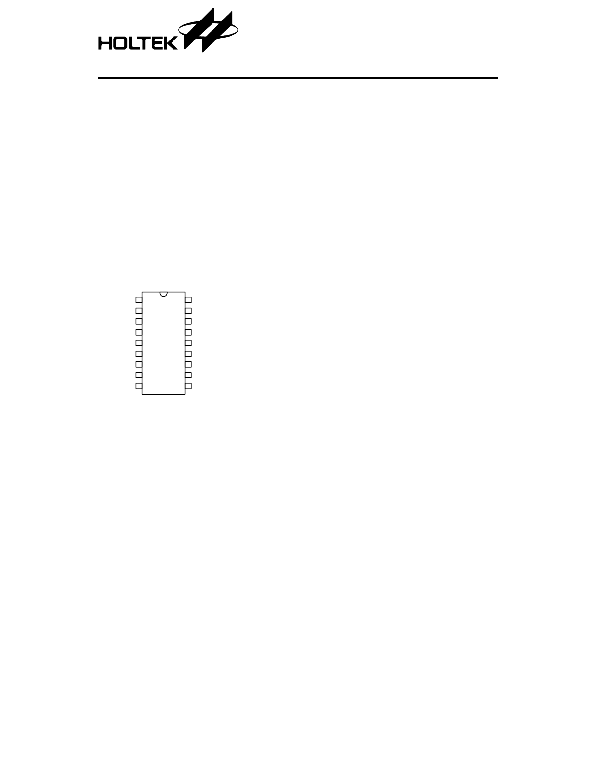
Pin Assignment
HT82M33A
3D Mous e Contro ller
•
Fit Plug and Play com port device specification
•
Z axis can support two kinds of scroller input (optomechanical and mechanical)
•
2MHz operating frequency with external
resonator
•
18-pin DIP package
support two kinds of scroller input, namely; optomechanical and mechanical.
Z1
Z2
RESET
MODE
OSCI
OSCO
CLOCK
DATA
VSS
18
1
17
2
16
3
15
4
14
5
13
6
12
7
11
8
10
9
HT82M33A
– 18 DIP
VDD
TEST
Y2
Y1
X2
X1
LB
Ro
RB
1 3rd Mar ’99
Pin Description
Pin No. Pin Name I/O Description
1,2 Z1, Z2 I
3 RESET I
4 MODE I
5 OSCI I “Oscillator in”: Connect to 2MHz crystal or resonator
6 OSCO O “Oscillator out”: Connect to 2MHz crystal or resonator
7 CLOCK I/O
8 DATA I/O
9 VSS I Negative power pin
10~12 RB, Ro, LB I
13~16
X1, X2,
Y1, Y2
17 TEST I
18 VDD I Positive power pin.
“Z axis input”: Supports two kinds of scroller input, optomechanical
and mechanical
“Reset input”: Resets internal circuit by input low, normal is
connected to high by internal pull-high resistor (120k
“MS or PS/2 mode selection”: Low for PS/2 mouse, high for MS
mouse. The MS PnP mouse ID code sure will appear when this pin
rise from low to high. Normal is connected to low by internal
pull-low resistor (60k
Ω). The mode input transition voltage is 2.0V.
“CLOCK I/O”: PS/2 mouse CLOCK line. NMOS open drain output
with 7.5k
Ω pull-high resistor.
“DATA/RXD I/O” PS/2 mouse DATA line or MS mouse
NMOS open drain output with 7.5k
“Right Button”: Normal pull-high (45k
“Rolling Button” : Norma l pull-high (45k
“Left Button”: Normal pull-high (45k
“X/Y axis input”: Auto level detecting inpu t. Any signal o ver 0.6V
I
V
is acceptable but the +VP cannot be over 2.5V
PP
Ω pull-high resistor.
Ω), press connect to low.
Ω), press connect to low.
Ω), press connect to low.
“IC test pin”: with built-in pull-low res istor. In normal operation
this is connected to VSS or floating. While the pin is connected to
VDD, this will provide the H/W test. The chip will accord the state
of the RB pin, to switch the X1/Y1 and X2/Y2 via th e PIN Ro an d
LB output.
HT82M33A
Ω).
RXD output.
Absolu te Maximu m R a tin g s
Supply Voltage.......................... ....–0.3V to 6.5V Storage Temperature.................–50°C to 125°C
Input V oltage................. V
Note: These are stress ratings only. Stresses exceeding the range specifie d under “Absolute Maxi-
mum Ratings” may cause substantial damage to the device. Functional operation of this device
at other conditions beyond those listed in the specification is not implied and prolonged
exposure to extreme condition s may affect device reliability.
–0.3V to VDD+0.3V Operating Temperature...............–25°C to 70°C
SS
2 3rd Mar ’99
HT82M33A
D.C. Characteristics Ta=25°C
Symbol Parameter
V
DD
I
SD
I
DD
V
IL
V
IH
V
IL1
V
IH1
V
IL2
V
IH2
V
IL3
V
IH3
I
OL
I
OH
R
L
R
L1
R
L2
R
L3
R
H
R
H1
Operating Voltage — — 4.5 5.0 5.5 V
Standby Voltage 5V RESET=0V, no load — — 1.5 mA
Operating Current 5V
Input Low Voltage
(RB, Ro, LB, TEST)
Input High Voltage
(RB, Ro, LB, TEST)
Input Low Voltage (Z1, Z2) 5V — 0 — 1.0 V
Input High Voltage (Z1, Z2) 5V — 1.2 — 5.0 V
Input Low Voltage
(CLOCK, DATA)
Input High Voltage
(CLOCK, DATA)
Input Low Voltage (RESET) 5V — 0 — 1.8 V
Input High Voltage (RESET) 5V — 3.3 — 5.0 V
Output Sink Current
(CLOCK, DATA)
Output Source Current
(CLOCK, DATA)
Pull-low Resistor (Z1, Z2) 5V VIH=5V, VSS=0V — 600 — kΩ
Pull-low Resistor (TEST) 5V VIH=5V, VSS=0V 10 17 30 kΩ
Pull-low Resistor (RB, Ro, LB) 5V VIH=5V,VSS=0V 33 45 56 kΩ
Pull-low Resistor (MODE) 5V VIH=5V,VSS=0V 48 60 72 kΩ
Pull-high Resistor
(CLOCK, DATA)
Pull-high Resistor ( RES ET) 5V VIL=0V 100 125 150 kΩ
Test Conditions
V
DD
Conditions
Freq=2MHz,
RESET=5V, no load
Min. Typ. Max. Unit
—2.23mA
5V — 0 — 1.5 V
5V — 3.5 — 5.0 V
5V — 0 — 1.2 V
5V — 2.1 — 5.0 V
5V V
5V V
5V V
=0.5V 6 — — mA
IL
=4.5V — 2 — mA
IH
=0V 5 7.5 10 kΩ
IL
3 3rd Mar ’99
HT82M33A
A.C. Characteristics Ta=25°C
Symbol Parameter
f
P
f
N
t
KD
t
MS
t
S
t
D
t
P
t
RD
t
R
t
F
t
RESET
F
OSC
X,Y Input Frequency 5V — — — 8.2 kHz
X,Y Operating Frequency 5 V — — — 8 kHz
Key Debounce 5V — — 52 — ms
Transmission Time 5 V Serial mouse mode — 33 — ms
Start Bit Time 5V Serial mouse mode — 0.85 — ms
Data Bit Time 5V Serial mouse mode — 0.82 — ms
Stop Bit Time 5V Serial mouse mode — 0.82 — ms
ID Code Delay 5V Serial mouse mode — 15 — ms
Rising Edge Crossed Width 5V — 50 — — µs
Falling Edge Crossed Width 5V — 50 — — µs
Reset Low Pulse Width 5V — 1 — — µs
System Clock 5V Crystal Oscillator — 2.0 — MHz
Test Conditions
V
DD
Conditions
Min. Typ. Max. Unit
4 3rd Mar ’99

HT82M33A
Functional Description
•
Serial mouse
•
Data format of 3D Serial mouse
1200 bps, N, 7, 1, single direction
Bit No. 6 5 4 3 2 1 0
1st word 1 L R Y7 Y6 X7 X6
2nd word 0 X5 X4 X3 X2 X1 X0
3rd word 0 Y5Y4Y3Y2Y1Y0
4th word 0 0 Ro Z3 Z2 Z1 Z0
Notes: X7~X0: -128<X<127, (2’s complement)
Y7~Y0: -128<Y<127, (2’s complement)
Z3~Z0: -8<Z<7, (2’s complement)
Button status:1=pressed, 0=released
Microsoft mode
Field Name Size Field Data Description
Old Mouse ID 1 4D
Compatible with Microsoft
Intelli mouse
Begin PnP 1 08 “(” indicates PnP IDs will follow
PnP Rev 2 01, 24 Identifiers PnP version 1.0
EISA ID 3 28, 34, 2B “HTK” (A mouse company)
Product ID 4 10, 10, 10, 11 “0001” (Unique product identifier)
Extended 1 3C “\”
Class Name 6 3C, 2D, 2F, 35, 33, 25
Driver ID 8
Checksum 2 19, 10
End PnP 1 09 “)” indicates PnP IDs complete
5 5A, 40, 00, 00, 00 “Z@”
3C, 30, 2E, 30, 10,
26, 10, 21
Win 95 Plug and Play ID fields
For compatibility with the old serial mouse
drivers, all mouse-compatible pointing devices must restrict themselves to a 6-bit character set, for all fields except the mo use ID.
Therefore, all old-mouse-compatible strings
are limited to values of 0
strings are ASCII codes from 0
offset by subtracting 0
Identifies a mouse for old Microsoft
mode drivers
“\MOUSE” fits a d efined Windows 95
class name
“\PNP0F0A” fits a defined Windows 95
Microsoft mouse compatible ID
Checksum of all characte rs from be gin
PnP to End PnP, exclusive of the
checksum characters themselves.
×00 to 0×3f; character
×20 to 0×5f,
×20.
5 3rd Mar ’99

•
Encourage the Plug and Play mouse ID
RTS
HT82M33A
RXD
PS/2 mouse
•
PS/2 status byte
15ms '4d 5a 40 00 00 00'+PnP ID stream
bit
7:RESERVED
6: 0=STREAM MODE, 1= REMOTE MODE
5: 0=DISABLED, 1=ENABLED
4: 0=SCALING 1:1, 1= SCALING 2:1
3: 1=WRAP MODE, 0=STREAM or REMOTE
(different from IBM spec.)
2: 1= LEFT BUTTON PRESSED
1: 1= MIDDLE BUTTON PRESSED
0: 1= RIGHT BUTTON PRESSED
•
Standard PS/2 data format
Variable rps, O, 8, 1, bidirectional, synchronous
Bit No. 7 6 5 4 3 2 1 0
1st word YV XV YS XS 1 M R L
2nd word X7 X6 X5 X4 X3 X2 X1 X0
3rd word Y7 Y6 Y5 Y4 Y3 Y2 Y1 Y0
•
Mouse mode changes between Standard a nd
3D PS/2 mode
Sending the commands in the following sequence will set the mouse to 3D PS/2 mode.
Command Response Fro m M ous e
F3h FAh
C8h FAh
F3h FAh
64h FAh
F3h FAh
50h FAh
F2h FAh, 03h
Any time the PC sends a reset “FFh” com-
*
mand to the mouse, it wil l reset the mou se
to Standard PS/2 mode.
After power on reset is initiated, the mouse
*
is set to Standard PS/2 mode.
•
Data format for 3D PS/2
Variable rps, O, 8, 1, bidirectional, synchronous
Bit No. 7 6 5 4 3210
1st word YV XV YS XS 1 Ro R L
2nd word X7 X6 X5 X4 X3 X2 X1 X0
3rd word Y7 Y6 Y5 Y4 Y3 Y2 Y1 Y0
4th word Z7 Z6 Z5 Z4 Z3 Z2 Z1 Z0
The x/y data report is 9-bit 2’s complement
The z data report is 8-bit 2’s complement
X move right is positive, move left is negative
Y move up is positive, move down is negative
Z rolling toward user is positive, else is negative
Button status : 1=pressed, 0=released
6 3rd Mar ’99

Timing Diagrams
X,Y,Z input
•
X,Y Axis Photo-coupler crossed width
X1 (Y1)
X2 (Y2)
T
R
•
Z Axis counting
Z1
Z2
+1 +1 +1+1 +1 +1 +1+1
Serial mouse
•
Word structure
HT82M33A
T
F
RXD
•
Key output
Key in/release
RXD
•
Bit structure
RXD
Data bit no.
1234
1
0
D
T
S
T
T
tms
D
4th word1st word 2nd word 3rd word
123 4
tms
2
3
4
5
6
D
D
D
D
T
T
T
DTDTP
T
T
7 3rd Mar ’99
1

•
Encourage the Plug and Play ID
RTS
t
RD
RXD
PnP ID4D PnP ID4D
•
PnP COM Enumerator timing
HT82M33A
t
RD
DTR
RTS
35ms
1st
setup
200ms
+35ms
1st
wait
200ms
+35ms
2nd
setup
T2T3 T4T2 T4
200ms
+35ms
2nd
wait
200ms
+35ms
ldle
check
dev
T1
200ms
35ms
+
200ms
+
T1: Interval to hold DTR high while waiting for DSR
T2: Interval for external device to power down or detect the port state
T3: DTR-RTS enumerator signature delay
T4: Maximum interval to wait for DSR and/or first received character
T5: PnP COM ID per/character timeout 200ms ( not shown )
T6: PnP COM ID EndPnP timeout 2.2 seconds ( not shown )
T7: Disconnect verification timeout 5 seconds ( not shown )
8 3rd Mar ’99

PS/2 mouse
•
Data output
HT82M33A
•
Data input
9 3rd Mar ’99

Application Circuits
HT82M33A 3D 2 in1 mouse (This application circuit is for reference only)
Clock/DTR
680pF
VDD
5.1V
100k
Ω
51k
Ω
10
µ
F
0.1
µ
F
1N4148
CLock/DTR
1N5871
VCC/RTS
Resonator
Reserve
for
1N4148
47pF
Ω
47pF1M
100
Ω
2MHz
1.5k
Ω
100k
Ω
HT82M33A
IR
51k
Ω
6
3
TXD
TXD
DATA
1
RXD
Data
47k
Ω
HT82M33A(X~Z)
8
9
DATA
VSS
VDD
RB
Ro
11
10
Button
Button
1.5k
Ω
CLOCK
LB
7
12
Button
IR
6
OSCI
OSCO
X2
X1
13
5
MODE
Y1
14
1
2
3
4
Z1
Z2
RESET
TEST
VDD
Y2
18
17
16
15
100k
Ω
1N4148
47k
Ω
1N4148
GND
3
SG5
4.7k
Ω
RXD
2
2
RXD
TXD
CLOCK/DTR
VCC/RTS
4
5
6
RTS7
DTR4DSR
47k
Ω
1µF
1N4148
IR
VDD
Notes: CLOCK & DAT A is internal pull-high 10kΩ.
OSCI & OSCO are build in R & C.
Z1 & Z2 is internal pull-low 250k
Ω.
10 3rd Mar ’99

HT82M33A 3D 2 in1 mouse (This application circuit is for reference only)
Clock/DTR
680pF
VDD
5.1V
1N4148
100
10
µ
F
0.1
µ
F
1N4148
CLock/DTR
1N5871
VCC/RTS
Resonator
Reserve
for
Ω
47pF
2MHz
Ω
47pF1M
HT82M33A
EVZVXC0012B
Encoder
6
3
TXD
TXD
6
DSR
TXD
CLOCK/DTR
5
4
DTR
100k
Ω
47k
Ω
1N4148
VCC/RTS
GND
3
4
7
RTS
SG5
1N4148
4.7k
Ω
RXD
2
2
RXD
DATA
1
Data
HT82M33A(X~Z)
47k
Ω
VDD
RXD
9
DATA
VSS
RB
Ro
10
Button
1.5k
Ω
8
CLOCK
LB
11
Button
IR
7
12
Button
OSCO
X1
5
6
MODE
OSCI
Y1
X2
14
13
1
2
3
4
Z1
Z2
RESET
TEST
VDD
Y2
18
17
16
15
47k
Ω
1
µ
F
1N4148
IR
VDD
Notes: CLOCK & DAT A is internal pull-high 10kΩ.
OSCI & OSCO are build in R & C.
Z1 & Z2 is internal pull-low 250k
Ω.
11 3rd Mar ’99

HT82M33A 3D PS2 mouse (This application circuit is for reference only)
1.5k
Ω
47pF
Resonator
Reserve
for
Ω
47pF1M
2MHz
CLOCK
DATA
HT82M33A
IR
HT82M33A(X~Z)
1
2
3
4
5
6
7
8
9
Z1
Z2
RESET
MODE
OSCI
OSCO
CLOCK
DATA
VSS
TEST
RB
Ro
LB
11
10
S2
S3
1.5k
Ω
Y1
X2
X1
14
13
12
S1
IR
VDD
Y2
18
17
16
15
IR
47k
Ω
1µF
1N4148
0.1
µ
F
VDD
12 3rd Mar ’99

HT82M33A 3D PS2 mouse (This application circuit is for reference only)
47pF
Resonator
Reserve
for
Ω
47pF1M
2MHz
CLOCK
DATA
EVZVXC0012B
Encoder
HT82M33A
HT82M33A(X~Z)
1
2
3
4
5
6
7
8
9
Z1
Z2
RESET
MODE
OSCI
OSCO
CLOCK
DATA
VSS
TEST
RB
Ro
LB
11
10
S2
S3
1.5k
Ω
Y1
X2
X1
14
13
12
S1
IR
VDD
Y2
18
17
16
15
IR
47k
Ω
1µF
1N4148
0.1
µ
F
VDD
13 3rd Mar ’99
 Loading...