


8-Bit Microcontroller with Voice ROM
Features
8-bit microcontroller
Operating voltage: 2.4V~5.2V
·
8K´16 program ROM
·
208´8 data RAM
·
36 bidirectional I/O lines
·
Interrupt input
·
16-bit programmable timer/event
·
counter with overflow interrupts
Watchdog timer
·
On-chip crystal or RC types of oscillator
·
Voice and melody synthesizer
128K´8 voice ROM
·
3/4 bit ADPCM coding algorithm
·
26 kinds of voice sampling rates
·
Tone level of 4 octaves
·
14 kinds of melody beats
·
Applications
Intelligent educational toys
·
High end toy controllers
·
Talking alarm clocks
·
HT827A0
Halt function and wake-up feature reduces
·
power consumption
63 powerful instructions
·
Up to a 1ms instruction cycle with a 4MHz
·
system clock at V
All instructions in 1 or 2 machine cycles
·
16-bit table read instruction
·
8-level subroutine nesting
·
Bit manipulation instruction
·
Current type of D/A switch output
·
Tone generator counter
·
Controllable volume
·
48-pin DIP package
·
Alert and warning systems
·
Public address systems
·
Sound effect generators
·
DD
=5V
General Description
The HT827A0 is 8-bit high performance
microcontroller with a voice synthesizer and
tone generator. They are designed for applications on multiple I/Os with sound effects. The
LSIs provide 26 kinds of voice sampling rates, 4
octaves of tone level as well as a high quality of
current type D/A output. With such a flexible
structure, the HT827A0 is excellent for versatile voice and sound effect product applications.
It also includes a halt function to reduce power
consumption.
1 March 15, 2000
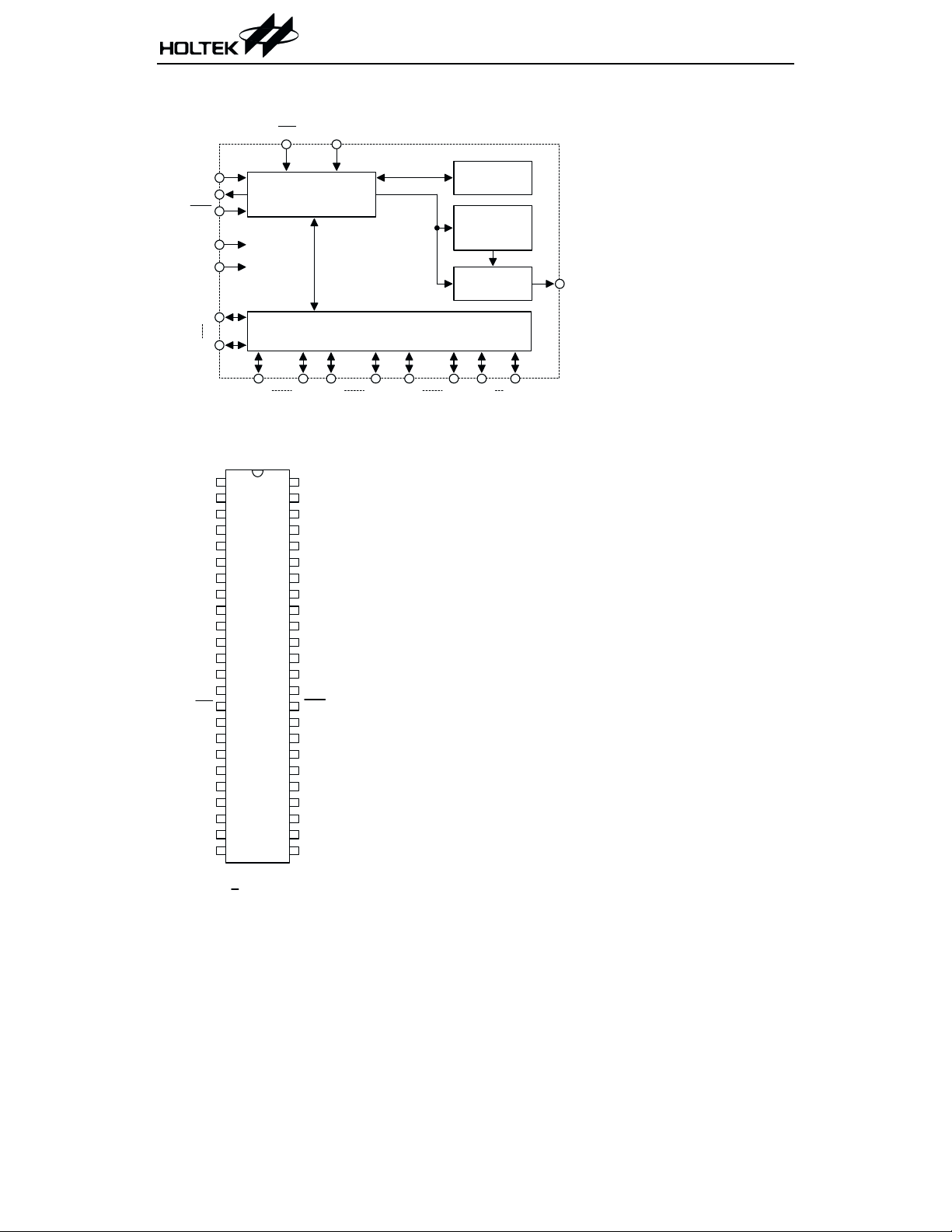
Block Diagram
IN T
HT827A0
TM R
OSC1
OSC2
8-bit H igh P erform ance
RES
VDD
VSS
PA0
PA7
PB0 PB7 PC0 PC7
Pin Assignment
PA3
1
PA2
2
3
PA1
4
NC
5
PA0
6
PB3
7
PB2
8
PB1
9
PB0
10
VSS
11
PE0
12
PE1
13
PE2
14
PE3
15
IN T
16
TM R
17
PD0
18
PD1
19
PD2
20
PD3
21
PD4
22
PD5
23
PD6
24
PD7
0 6& %)
"&, 12
M icrocontroller
48
PB4
PB5
47
46
PB6
45
PB7
44
PA4
43
PA5
42
PA6
41
PA7
40
NC
39
NC
38
NC
37
OSC2
36
OSC1
35
VDD
34
RES
33
AUD
32
PC7
31
PC6
30
PC5
29
PC4
28
PC3
27
PC2
26
PC1
25
PC0
36-bit Bidirectional
I/O P o r ts
PD0 PD7 PE0 PE3
Voice RO M
& C ontroller
Voice
Synthesizer &
Tone generator
C urrent T ype
D/A Output
AUD
2 March 15, 2000
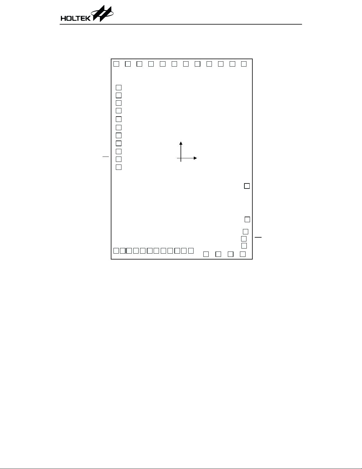
Pad Assignment
HT827A0
PA7
PB4
PA3
PA2
PA1
PA0
PB6
PB5
PA4
PB7
PA6
PA5
1
PB3
PB2
PB1
PB0
VSS
PE0
PE1
PE2
PE3
IN T
TM R
13 14 15 16 17
PD0
2
3
4
5
6
7
8
9
10
11
12
44
PD2
PD1
42 43
41
19
18
20 21 22
PD7
PD6
PD5
PD4
PD3
39 40
(0 ,0 )
23 24
PC3
PC2
PC1
PC0
25 26
PC5
PC4
36 37 38
35
34
33
OSC2
32
OSC1
31
VDD
30
RES
AUD
29
28
27
PC7
PC6
Chip size: 3555 ´ 5015 (mm)
2
* The IC substrate should be connected to VSS in the PCB layout artwork.
* The TMR pad must be bound to VDD or VSS if it is not used.
3 March 15, 2000
HT827A0
Pad Coordinates
Pad No. X Y Pad No. X Y
10
11
12
13
14
15
16
17
18
19
20
21
22
1
2
3
4
5
6
7
8
9
-1543.05
-1486.75
-1486.75
-1486.75
-1486.75
-1486.75
-1486.75
-1486.75
-1486.75
-1486.75
-1486.75 -28.35
-1486.75 -219.25
-1547.75 -2211.75
-1389.55 -2211.75
-1239.35 -2211.75
-1072.15 -2211.75
-913.45 -2211.75
-744.65 -2211.75
-585.95 -2211.75
-417.15 -2211.75
-258.45 -2211.75
-89.65 -2211.75
2242.95 23 69.05
1675.25 24 237.85
1491.25 25 598.35
1308.95 26 890.95
1126.15 27 1184.35
925.35 28 1476.95
727.25 29 1507.85
538.35 30 1499.05
347.85 31 1539.95
157.35 32 1585.75
33 1574.15
34 1502.55 2242.95
35 1227.35 2242.95
36 951.35 2242.95
37 676.15 2242.95
38 396.95 2242.95
39 119.35 2242.95
40
41
42
43
44
-159.85
-437.45
-716.65
-991.85
-1267.85
Unit: mm
-2211.75
-2211.75
-2291.45
-2291.45
-2291.45
-2291.45
-2091.35
-1925.15
-1757.35
-1465.55
-667.75
2242.95
2242.95
2242.95
2242.95
2242.95
Pad Description
Pad No. Pad Name I/O
1, 44~42,
37~34
5~2,
41~38
21~28 PC0~PC7 I/O
PA0~PA7 I/O
PB0~PB7 I/O
Mask
Option
Wake-up
Pull-high
or None
Pull-high
or None
Pull-high
or None
Description
Bidirectional 8-bit input/output ports
Each bit can be configured as a wake-up input by mask
option. Software instructions determine the CMOS output or schmitt trigger input with or without a pull-high resistor (mask option).
Bidirectional 8-bit input/output ports
Software instructions determine the CMOS output or
schmitt trigger input with or without a pull-high resistor
(mask option).
Bidirectional 8-bit input/output ports
Software instructions determine the CMOS output or
schmitt trigger input with or without a pull-high resistor
(mask option).
4 March 15, 2000
HT827A0
Pad No. Pad Name I/O
13~20 PD0~PD7 I/O
6 VSS
7~10 PE0~PE3 I/O
11 INT
12 TMR I
29 AUD O
30 RES
31 VDD
32
33
OSC1
OSC2
¾¾
I
I
¾¾
IOCrystal or
Mask
Option
Pull-high
or None
Pull-high
or None
¾
¾
¾
¾
RC
Description
Bidirectional 8-bit input/output ports
Software instructions determine the CMOS output or
schmitt trigger input with or without a pull-high resistor
(mask option).
Negative power supply, ground
Bidirectional 8-bit input/output ports
Software instructions determine the CMOS output or
schmitt trigger input with or without a pull-high resistor
(mask option).
External interrupt schmitt trigger input with a
pull-high resistor
Edge triggered is activated on a high to low transition.
Schmitt trigger input for a timer/event counter
Audio output for driving an external transistor
PMOS open drain output
Schmitt trigger reset input, active low
Positive power supply
OSC1 and OSC2 connect to an RC network or crystal os
cillator (determined by mask option) for an internal sys
tem clock. In the case of RC operation, an oscillation
resistor connects to OSC1. OSC2 is the output terminal
of a 1/4 system clock.
-
-
Absolute Maximum Ratings
Supply Voltage..............................-0.3V to 5.5V
Input Voltage.................V
Note: These are stress ratings only. Stresses exceeding the range specified under ²Absolute Maxi
mum Ratings² may cause substantial damage to the device. Functional operation of this de
vice at other conditions beyond those listed in the specification is not implied and prolonged
exposure to extreme conditions may affect device reliability.
-0.3V to VDD+0.3V
SS
Storage Temperature.................-50°Cto125°C
Operating Temperature ..............-25°Cto70°C
5 March 15, 2000
-
-
HT827A0
D.C. Characteristics
Symbol Parameter
V
DD
I
DD1
I
DD2
I
STB1
I
STB2
V
IL
V
IH
V
IL1
V
IH1
I
OL1
I
OH1
I
OL2
I
OH2
R
PH
I
O
Operating Voltage
Operating Current (Crystal OSC)
Operating Current (RC OSC)
Standby Current (WDT Enabled)
Standby Current (WDT Disabled)
Input Low Voltage for I/O Ports
Input High Voltage for I/O Ports
Input Low Voltage
(RES
, TMR, INT)
Input High Voltage
(RES
, TMR, INT)
I/O Port Sink Current
(PA, PC, PD, PE)
I/O Port Source Current
(PA, PC, PD, PE)
PB Sink Current
PB Source Current
Pull-high Resistance of I/O Ports
& INT
Max. AUD Output Current
Test Conditions
V
DD
Conditions
¾¾
3V
No load,
=4MHz
f
SYS
5V
3V
No load,
=4MHz
f
SYS
5V
3V
No load,
system Halt
5V
3V
No load,
system Halt
5V
3V
5V
3V
5V
3V
5V
3V
5V
3V
5V
3V
5V
3V
5V
3V
5V
3V
5V
3V
5V
¾
¾
¾
¾
¾
¾
¾
¾
V
=0.3V
OL
=0.5V
V
OL
V
=2.7V
OH
V
=4.5V
OH
V
=0.3V
OL
V
=0.5V
OL
V
=2.7V
OH
V
=4.5V
OH
¾
¾
V
=0.6V
OH
V
=0.6V
OH
Ta=25°C
Min. Typ. Max. Unit
2.4
1.5 3 mA
¾
¾
1.5 3 mA
¾
2.5 5 mA
¾
¾¾
¾¾
¾¾
¾¾
0
0
2.4
4.0
0
0
2.4
4.0
24
610
-1 -1.5 ¾
-2 -4 ¾
610
20 25
-0.5 -1 ¾
-1 -2 ¾
25 50 100
10 30 60
-1.5 -2 ¾
-3.5 -4 ¾
5.2 V
¾
35mA
10
mA
20
mA
3
mA
5
mA
0.6 V
¾
1.0 V
¾
¾
¾
¾
¾
¾
¾
3V
5V
0.6 V
1.0 V
3V
5V
mA
¾
mA
¾
mA
mA
mA
¾
mA
¾
mA
mA
kW
kW
mA
mA
6 March 15, 2000
HT827A0
A.C. Characteristics
Symbol Parameter
f
SYS1
f
SYS2
f
TIMER
t
WDTOSC
t
WDT1
t
WDT2
t
RES
t
INT
Note: t
System Clock (Crystal OSC)
System Clock (RC OSC)
Timer I/P Frequency (TMR)
Watchdog Oscillator 5V
Watchdog Timeout Period (RC) 5V
Watchdog Timeout Period
(System Clock)
External Reset Low Pulse Width 5V
Interrupt Pulse Width 5V
SYS
=1/(f
SYS
)
Test Conditions
DD
Conditions
¾
¾
¾
¾
¾
¾
V
3V
5V
3V
5V
3V
5V
¾
Without WDT
prescaler
Without WDT
5V
prescaler
¾
¾
Ta=25°C
Min. Typ. Max. Unit
400
400
400
400
0
0
31 78 140
¾
¾
¾
¾
¾
¾
4000 kHz
4000 kHz
4000 kHz
4000 kHz
4000 kHz
4000 kHz
ms
82036ms
¾
1024
1
¾¾ms
1
¾¾ms
¾
t
SYS
7 March 15, 2000
Functional Description
Executive flow
The HT827A0 provides a system clock which is
derived from a crystal or an RC type of oscillator.
The clock is internally divided into four
non-overlapping clocks denoted by P1, P2, P3 and
P4. An instruction cycle consists of T1~T4.
Instruction fetching and execution are
pipelined in such a way that a fetch takes an in
struction cycle while decoding and execution
take the next instruction cycle. The pipelining
scheme causes each instruction to execute ef
fectively in a cycle. If an instruction changes
the program counter, two cycles are required to
complete that instruction.
Program counter - PC
The program counter (PC) controls the se
quence in which the instructions stored in the
program ROM are executed.
The contents of the program counter are incre
mented by one after a program memory word is
accessed to fetch an instruction code. The pro
gram counter then points to a memory word
containing the next instruction code.
The PC manipulates a program transfer by
loading the address corresponding to each in
struction when executing a jump instruction,
conditional skip execution, loading PCL regis
ter, subroutine call, initial reset, internal inter
rupt, external interrupt or return from
-
subroutine.
The conditional skip is activated by instructions.
Once the condition is satisfied, the next instruc
tion, fetched during the current instruction exe
cution, is discarded and a dummy cycle replaces
it to get a proper instruction. Otherwise, the sys
tem will proceed with the next instructions.
The lower byte of the program counter (PCL) is
a readable and writable register (06H). Moving
data into PCL performs a short jump. The desti
nation is within 256 locations.
Once a control transfer takes place, the execu
tion suffers from an additional dummy cycle.
-
HT827A0
-
-
-
-
-
-
-
-
S yste m C lock
OSC2 (RC only)
P1
P2
P3
P4
PC
T1 T2 T3 T4 T1 T2 T3 T4 T1 T2 T3 T4
PC PC+1 PC+2
F e tc h IN S T (P C )
Execute IN S T (P C -1)
F e tc h IN S T (P C + 1 )
Execute IN S T (P C )
F e tc h IN S T (P C + 2 )
Execute IN S T (P C +1)
Execution flow
8 March 15, 2000
Internal
Phase
C lo cks
HT827A0
Program memory - ROM
The program memory stores the to-be-executed
program instructions. It also includes data, ta
ble and interrupt entries, addressed by the pro
gram counter along with the table pointer.
The program memory size for HT827A0 is
8K´16.
Certain locations in the program memory are
reserved for special usage:
·
Location 000H
This area is reserved for program initializa
tion. The program always begins execution at
location 000H each time the system is reset.
·
Location 004H
This area is reserved for an external interrupt
service program. The program begins execu
tion at location 004H if the INT
input pin is
activated, the interrupt is enabled and the
stack is not full.
·
Location 008H
This area is reserved for a voice sampling rate
counter interrupt service program. The pro
gram begins execution at location 008H if a
timer interrupt results from a sampling rate
000H
004H
-
-
-
008H
00C H
1FFFH
D evice initialization program
External interrupt subroutine
Sam pling rate counter interrupt subroutine
Tim er/event counter interrupt subroutine
Look-up table (256 w ords)
Look-up table (256 w ords)
Program
ROM
Program memory
counter overflow, the interrupt is enabled and
the stack is not full.
-
·
Location 00CH
This area is reserved for a timer/event coun
ter interrupt service program. The program
begins execution at location 00CH if an inter
rupt results from a timer/event counter over
-
flow, the interrupt is enabled and the stack is
-
not full.
Mode
*12 *11 *10 *9 *8 *7 *6 *5 *4 *3 *2 *1 *0
Program Counter
Initial reset 00000000000 0 0
External interrupt 00000000001 0 0
Sampling rate counter
overflow
Timer/event counter
overflow
00000000010 0 0
00000000011 0 0
Skip PC+2
Loading PCL *12 *11 *10 *9 *8 @7 @6 @5 @4 @3 @2 @1 @0
Jump, call branch #12 #11 #10 #9 #8 #7 #6 #5 #4 #3 #2 #1 #0
Return from subroutine S12 S11 S10 S9 S8 S7 S6 S5 S4 S3 S2 S1 S0
Program counter
Note: *12~*0: Bits of program counter S12~S0: Bits of stack register
#12~#0: Bits of instruction code @7~@0: Bits of PCL
9 March 15, 2000
HT827A0
·
Table location
Any location in the program ROM can be used
as a look-up table. The instructions
²TABRDC [m]² (the current page, 1 page=256
words) and ²TABRDL [m]² (the last page)
transfer the contents of the lower-order byte
to the specified data memory, and the
higher-order byte to TBLH (08H). Only the
destination of the lower-order byte in the ta
ble is well-defined. The other bits of the table
word are transferred to the lower portion of
TBLH. The higher-order byte register
(TBLH) of the table is read only. The table
pointer (TBLP), on the other hand, is a
read/write register (07H) indicating the table
location. This location must be placed in
TBLP before accessing the table. All the table
related instructions require 2 cycles to com
plete an operation. These areas may function
as a normal program memory depending
upon the user¢s requirements.
Stack register - Stack
The stack register is a special part of the mem
ory used to save the contents of the program
counter (PC). This stack is organized into 8 levels. It is neither part of the data nor program
space, and cannot be read or written to. Its activated level is indexed by a stack pointer (SP)
and cannot be read or written to. At a subroutine call or interrupt acknowledgment, the contents of the program counter are pushed onto
the stack. The program counter is restored to
its previous value from the stack at the end of a
subroutine or interrupt routine, which is signaled by a return instruction (RET or RETI).
After a chip resets, SP will point to the top of
the stack.
The interrupt request flag will be recorded but
the acknowledgment will be inhibited when the
stack is full and a non-masked interrupt takes
place. After the stack pointer is decremented
(by RET or RETI), the interrupt will be ser
viced. This feature prevents stack overflow and
allows programmers to use the structure more
easily. In a similar case, if the stack is full and a
²CALL² is subsequently executed, stack over
flow occurs and the first entry is lost.
Data memory - RAM
The data memory is further divided into two
functional groups, namely, special function reg
isters and general purpose data memories. Al
though most of them can be read or be written
to, some are read only.
The data memory size for HT827A0 is shown as
follows.
Pard No.
HT827A0 00H~2FH 30H~FFH
The special function registers include an indi
rect addressing register (00H), timer/event
counter high byte register (TMRH; 0FH),
timer/event counter low byte register (TMRL;
10H); timer/event counter control register
(TMRC; 11H), program counter lower-order
byte register (PCL; 06H), memory pointer register (MP; 01H), accumulator (ACC; 05H), table
pointer (TBLP; 07H), table higher-order byte
register (TBLH; 08H), status register
(STATUS; 0AH), interrupt control register
(INTC; 0BH), watchdog timer option setting
register (WDTS; 09H), I/O registers (PA; 12H,
PB; 14H, PC; 16H, PD; 18H, PE; 1AH) and I/O
Special
RAM
RAM Address
-
-
-
-
General
-
Instruction(s)
TABRDC [m] P12 P11 P10 P9 P8 @7 @6 @5 @4 @3 @2 @1 @0
TABRDL [m] 1 1 1 1 1 @7 @6 @5 @4 @3 @2 @1 @0
Note: *12~*0: Bits of table location P12~P8: Bits of current program counter
@7~@0: Bits of table pointer
*12 *11 *10 *9 *8 *7 *6 *5 *4 *3 *2 *1 *0
Table Location
Table location
10 March 15, 2000
HT827A0
Ind irect A dd ressing R e giste r
00H
01H
02H
03H
04H
05H
06H
07H
08H
09H
0AH
0BH
0C H
0D H
0EH
0FH
10H
11H
12H
13H
14H
15H
16H
17H
18H
19H
1AH
1BH
1C H
1D H
1EH
1FH
20H
21H
22H
23H
24H
25H
26H
27H
28H
29H
2AH
2BH
2C H
2D H
2EH
2FH
30H
G eneral P urpose
DATA M EM ORY
FFH
MP
ACC
PCL
TBLP
TBLH
WDTS
STATUS
IN T C
TM R H
TM R L
TM RC
PA
PAC
PB
PBC
PC
PCC
PD
PDC
PE
PEC
DAL
DAH
VCR
SRC
BEAT
TEM PO
TO N E
ROM C
RAM mapping
Special P urpose
DATA M EM ORY
: U n u s e d
R ead as "00"
control registers (PAC; 13H, PBC; 15H, PCC;
17H, PDC; 19H, PEC; 1BH). The 20H to 2FH
are used for sound and tone (melody) synthesis.
The function registers include a lower-order
byte register (DAL; 20H) of D/A data,
higher-order byte register (DAH;21H) of D/A
data , volume control register (VCR; 22H), sam
pling rate control register (SRC; 23H), beat con
trol register (BEAT; 28H), tempo control
register (TEMPO; 29H), tone control register
(TONE; 2AH) and voice ROM control register
(ROMC; 2CH). The remaining space before 30H
is reserved for future expansion. Reading these
remaining locations will get ²00H². The general
purpose data memory is used for data and con
trol information under instruction commands.
All of the areas of data memory can handle
arithmetic, logic, increment, decrement and ro
tate operations directly. Except for some dedi
cated bits, each bit in the data memory can be
set and reset by ²SET [m].i² and ²CLR [m].i²,
and can also be indirectly accessed through a
memory pointer register (MP; 01H).
Indirect addressing register
Location 00H is an indirect addressing register
that is not physically implemented. Any
read/write operation of [00H] accesses the data
memory pointed to by MP (01H). Indirectly reading location 00H will return the result to 00H
whereas, indirectly writing it will have no effect.
Arithmetic and logic unit - ALU
This circuit performs 8-bit arithmetic and logic
operations. ALU provides the following functions:
·
Arithmetic operations (ADD, ADC, SUB,
SBC, DAA)
·
Logic operations (AND, OR, XOR, CPL)
·
Rotation (RL, RR, RLC, RRC)
·
Increment & decrement (INC, DEC)
·
Branch decision (SZ, SNZ, SIZ, SDZ ....)
ALU not only saves the results of a data opera
tion but also change the status register.
-
-
-
-
-
-
11 March 15, 2000

HT827A0
Status register - STATUS
This 8-bit register (0AH) consists of a zero flag
(Z), carry flag (C), auxiliary carry flag (AC),
overflow flag (OV), power down flag (PD) and
watchdog time-out flag (TO). It also records the
status information and controls the operation
sequence.
Except the TO and PD flags, bits in the status
register can be altered by instructions similar to
other registers. Any data written into the status
register will not change the TO or PD flag. Opera
tions related to the status register may yield dif
ferent results from those intended. The TO and
PD flags can be altered only by a watchdog timer
overflow, chip power-up, clearing the watchdog
time or executing the ²HALT² instruction.
The Z, OV, AC and C flags generally reflect the
statuses of the latest operations.
The status register will not be pushed onto the
stack automatically on entering the interrupt
sequence or executing the subroutine call. If the
status contents are important and the subrou
tine may corrupt the status register, the pro
grammer must take precautions and save it
properly.
Labels Bits Function
C is set if an operation results in a carry during an addition operation or if a bor-
C0
AC 1
Z2
OV 3
PD 4
TO 5
¾
¾
row does not take place during a subtraction operation; otherwise C is cleared. It
is also affected by a rotate through carry instruction.
AC is set if the operation results in a carry out of the low nibbles in addition or if
no borrow from the high nibble into the low nibble in subtraction takes place;
otherwise AC is cleared.
Z is set if the result of an arithmetic or logic operation is zero; otherwise Z is
cleared.
OV is set if an operation results in a carry into the highest-order bit but not a
carry out of the highest-order bit, or vice versa, otherwise OV is cleared.
PD is cleared by a system power-up or executing the ²CLR WDT² instruction.
PD is set by executing the ²HALT² instruction.
TO is cleared by a system power-up or executing the ²CLR WDT² or ²HALT² in
structions. TO is set by a WDT time-out.
6
Undefined, read as ²0²
7
Undefined, read as ²0²
Interrupt
The HT827A0 provides an external interrupt in
addition to two internal timer/event counter in
terrupts. The interrupt control register (INTC;
0BH) includes interrupt control bits to set the
enable/disable and the interrupt request flags.
Once an interrupt subroutine is serviced, all
the other interrupts will be blocked (by clear
ing the EMI bit). This scheme may prevent any
further interrupt nesting. Other interrupt re
quests may happen during this interval but
only the interrupt request flag is recorded. If
an interrupt needs servicing within the ser
vice routine, the programmer may set the EMI
bit and the corresponding bit of INTC, allow
ing interrupt nesting. If the stack is full, the
interrupt request will not be acknowledged till
the SP is decremented, whether or not the re
lated interrupt is enabled. If immediate ser
vice is desired, the stack has to be prevented
from becoming full.
All these interrupts have a wakeup capability.
As an interrupt is serviced, a control transfer
occurs by pushing the program counter onto the
-
-
-
-
-
-
-
-
STATUS register
12 March 15, 2000

HT827A0
stack and then branching to subroutines at the
specified location(s) in the program memory.
Only the program counter is pushed onto the
stack. The programmer must save the contents
of the register or status register (STATUS) in
advance if they are altered by an interrupt ser
vice program which corrupts the desired con
trol sequence.
External interrupts are triggered by a high to
low transition of INT
quest flag (EIF; bit 4 of INTC) are also set.
When an interrupt is enabled, the stack is not
full and the external interrupt is active, a sub
routine call to location 04H will occur. The in
terrupt request flag (EIF) and EMI bits will be
cleared to disable other interrupts.
The sampling rate counter interrupt is initial
ized by setting a sampling rate counter inter
rupt request flag (SRF; bit 5 of INTC), which is
caused by a timer overflow. When an interrupt
is enabled, the stack is not full and the SRF bit
is set, a subroutine call to location 08H will oc
cur. The related interrupt request flag (SRF)
will be reset and the EMI bit be cleared to dis
able further interrupts.
. The related interrupt re
The internal timer/event counter interrupt is
initialized by setting a timer/event counter in
terrupt request flag (TF; bit 6 of INTC), which
is caused by a timer overflow. When an inter
rupt is enabled, the stack is not full and the TF
bit is set, a subroutine call to location 0CH will
occur. The related interrupt request flag (TF)
will be reset and the EMI bit will be cleared to
disable further interrupts.
During the execution of an interrupt subrou
tine, other interrupt acknowledgments are all
held until the ²RETI² instruction is executed or
-
the EMI bit and the related interrupt control
-
bit are set to 1 (if the stack is not full). To return
from an interrupt subroutine, ²RET² or ²RETI²
may be invoked. RETI will set the EMI bit to
enable an interrupt service, but RET will not.
-
-
Interrupts occurring in an interval between the
rising edges of two consecutive T2 pulses will be
serviced at the latter of the two T2 pulses if the
corresponding interrupts are enabled. In the
-
case of simultaneous requests, they can be
masked by resetting the EMI bit. The following
-
table illustrates the priority of applying the si
multaneous requests:
-
-
-
-
Register Bit No. Label Function
Controls a master (global) interrupt
(1=enabled; 0=disabled)
Controls an external interrupt
(1=enabled; 0=disabled)
Controls a sampling rate counter interrupt
(1=enabled; 0=disabled)
Controls a timer/event counter interrupt
(1=enabled; 0=disabled)
External interrupt request flag
(1=active; 0=inactive)
Sampling rate counter request flag
(1=active; 0=inactive)
Internal timer/event counter request flag
(1=active; 0=inactive)
INTC register
13 March 15, 2000
INTC
(0BH)
0 EMI
1 EEI
2 ESI
3 ETI
4 EIF
5 SRF
6TF
7
¾ Unused bit, read as ²0²

HT827A0
No.
Interrupt
Source
Priority Vector
a External Interrupt 1 04H
Sampling Rate
b
Counter Overflow
Timer/Event
c
Counter Overflow
2 08H
3 0CH
The timer/event counter interrupt request flag
(TF), external interrupt request flag (EIF), sam
pling rate counter interrupt request flag (SRF),
enable timer/event counter bit (ETI), enable ex
ternal interrupt bit (EEI), enable sampling rate
counter bit (ESI) and enable master interrupt bit
(EMI) make up an interrupt control register
(INTC) which is located at 0BH in the data mem
ory. EMI, EEI, ESI and ETI are used to control
the enable/disable status of interrupts. These bits
prevent the requested interrupt from being ser
viced. Once the interrupt request flags (TF, SRF,
EIF) are all set, they will remain in the INTC reg
ister till the interrupts are serviced or cleared by
a software instruction.
The ²CALL subroutine² is preferably not used
within the interrupt subroutine. This is because
interrupts often occur in an unpredictable manner or required to be serviced immediately in certain applications. If only one stack is left and
enabling the interrupt is not well controlled, operation of the ²call² in the interrupt subroutine
will damage the original control sequence.
Oscillator configuration
The HT827A0 provides two kinds of oscillator circuits, namely, RC and crystal oscillators, for system clocks. Selection of the oscillator circuit
type is determined by mask option. When the
device enters the HALT mode, the system oscil
lator stops to conserve power. The system clock
is later reset with an external signal.
If an RC type of oscillator is used, an external
resistor between OSC1 and GND is required
and the range of the resistance has to be from
51kW to 1MW. The system, divided by 4, is
available on OSC2, which synchronizes exter
nal logic. The RC type of oscillator provides the
most cost-effective solution. Nonetheless, the
OSC1
OSC2
C rystal O scilla to r
f
SYS
/4
System oscillator
frequency of the oscillation may vary with
VDD, temperature and the chip itself due to
process variations. It is, therefore, not suitable
for timing sensitive operations where an accu
rate oscillator frequency is demanded.
On the other hand, if a crystal type of oscillator
is used instead, a crystal across OSC1 and OSC2
is required, providing feedback and phase shift
for the oscillator. No other external components
are needed. The resonator can replace the crys
tal and connects between OSC1 and OSC2 so
that a frequency reference can be derived. But
two external capacitors in OSC1 and OSC2 are
required.
The WDT oscillator is a free running on-chip RC
oscillator, requiring no external components. The
WDT oscillator still works a period of approximately 78ms even when the system enters the
power down mode and the system clock is terminated. It nonetheless can be disabled by mask option for conserving power.
Watchdog timer - WDT
The clock source of WDT is implemented by a
dedicated RC oscillator (WDT oscillator) or instruction clock (system clock divided by 4), de
cided by mask option. The watchdog timer is
designed to prevent a software malfunction or
sequence jumping to an unknown location with
unpredictable results. It can be disabled by
mask option. After it is disabled, all executions
related to WDT are ignored.
WDT is first divided by 256 (8 stages) to get a
nominal time-out period of 20 ms once an inter
nal WDT oscillator (RC type of oscillator nor
mally with a period of 78ms) is selected. This
time-out period may vary with temperature,
VDD and process variations. By invoking the
OSC1
OSC2
R C O scillator
-
-
-
-
-
14 March 15, 2000
HT827A0
WDT prescaler, a longer time-out period can be
attained. Writing data to WS2, WS1 and WS0
(bits 2, 1 and 0 of WDTS) can derive different
time-out periods. If WS2, WS1 and WS0 are all
equal to 1, the division ratio is up to 1:128, and
the maximum time-out period is 2.6 seconds.
WS2 WS1 WS0 Division Ratio
000 1:1
001 1:2
010 1:4
011 1:8
1 0 0 1:16
1 0 1 1:32
1 1 0 1:64
1 1 1 1:128
WDTS register
If the WDT oscillator is disabled, the WDT clock
may still come from an instruction clock. It oper
ates in the same manner except that WDT may
stop counting and loses its protecting purpose in
the HALT state. In this situation the logic can
only be re-initialized by external logic. The high
nibble and bit 3 of WDTS are reserved for user¢s
defined flags. The programmer may use these
flags to indicate some specified statuses.
The on-chip RC oscillator (WDT OSC) is
strongly recommended if the device operates in
a noisy environment, since the HALT function
will stop the system clock.
Overflow of the WDT under a normal operation
initializes a ²chip reset² and sets the status bit
²TO². It will initialize a ²warm reset², and only
PC and SP are reset to zero in the HALT mode.
To clear the contents of WDT (including the
WDT prescaler), three methods are adopted,
namely, external reset (a low level to RES
software instructions, and ²HALT² instruction.
The software instructions include ²CLR WDT²
and the other sets -²CLR WDT1² and ²CLR
WDT2². Of these two types of instructions, by
mask option only one can be active at a time ²CLR WDT times selection option².If²CLR
WDT² is chosen (i.e., CLRWDT times equal
one), any execution of the ²CLR WDT² instruc
tion will clear WDT. In the case that ²CLR
WDT1² and ²CLR WDT2² are selected (i.e.,
CLRWDT times equal two), these two instruc
tions must be executed to clear WDT; otherwise
WDT may reset the chip as a result of time-out.
Power down operation - HALT
The HALT mode is initialized by the ²HALT²
instruction and results in the following:
·
-
The system oscillator is turned off but the
WDT oscillator still keeps running (if the
WDT oscillator is selected).
·
The contents of the on-chip RAM and regis
ters remain unchanged.
·
The WDT and WDT prescaler are cleared and
re-counted (if the clock of WDT is from the
WDT oscillator).
·
All the I/O ports maintain their original
statuses.
·
The PD flag is set and the TO flag cleared.
The system can quit the HALT mode by an external reset, interrupt, external falling edge signal
on port A or WDT overflow. An external reset
leads to device initialization and a WDT overflow
performs a ²warm reset². The reason for chip re
),
-
-
-
-
S yste m C lock/4
WDT
OSC
Mask
Option
S e le c tio n
W D T P rescale r
8-bit C ounter
7-bit C ounter
8 -to -1 M U X
W D T Tim e-out
WS0~WS2
Watchdog timer
15 March 15, 2000

HT827A0
set can then be determined after examining the
TO and PD flags. The PD flag is cleared when the
system powers up or executes the ²CLR WDT²in
struction and set when the ²HALT² instruction is
executed. The TO flag is set if the WDT time-out
occurs, and causes a wake-up that resets only the
PC and SP. The others maintain their original
statuses.
The port A wake-up and interrupt methods can
be considered as a continuation of normal exe
cution. Each bit in port A can be independently
selected to wake up the device by mask option.
Awakening from an I/O port stimulus, the pro
gram resumes execution of the next instruc
tion. However, if it is awakening from an
interrupt, two sequences may happen. The pro
gram will resume execution at the next instruc
tion if the related interrupt is disabled or the it
is enabled but the stack is full. Nonetheless, if
the interrupt is enabled and the stack is not
full, a regular interrupt response takes place.
Once the wake-up event occurs, and the system
clock comes from a crystal, it takes 1024 t
SYS
(system clock period) to resume a normal opera
tion. In other words, the HT827A0 will insert a
dummy period after the wake-up. If the system
clock, on the other hand, is from an RC type of
oscillator, it will continue operation. The actual
interrupt subroutine execution will be delayed
by one or more cycles if the wake-up results
from an interrupt acknowledgment. On the
other hand, it will be executed immediately after the dummy period is finished if the wake-up
results in the next instruction execution.
To minimize power consumption, all the I/O
pins should be carefully managed before entering the HALT mode.
Reset
There are threeways in whicha reset can occur:
·
RES reset during normal operation
·
RES reset during HALT
·
WDT time-out reset during a normal operation
The WDT time-out during HALT is different
from other chip reset conditions, since it can
perform a ²warm reset² that resets only the PC
and SP, leaving the other circuits to remain in
their original states. Some registers will re
main unchanged during reset conditions. Most
registers are reset to the ²initial condition² once
the reset conditions are met. The program can
distinguish between different ²chip resets² by
examining the PD flag and TO flag.
TO PD RESET Conditions
0 0 RES
-
-
-
uu
0 1 RES
1u
reset during power-up
reset during normal
RES
operation
wake-up HALT
WDT time-out during normal
operation
-
-
11
WDT wake-up HALT
Note: ²u² means ²unchanged²
To guarantee that the crystal oscillator is
started and stabilized, XST (Crystal Start-up
Timer) provides an extra-delay by an OSC
mask option. The extra-delay delays 1024 sys
tem clock pulses when the system awakes from
the HALT state or from system power-up and
the RES
transforms low to high. XST is auto
matically selected if the crystal oscillator is invoked. On the other hand, it is disabled when
the RC oscillator is chosen. The XST delay is
added after XST is chosen and awakening from
the HALT state or the system powers up.
The reset duration comes only from RES
RC oscillator is selected. An extra delay, on the
other hand, is added during the power-up period and any wakeup from HALT only if a crystal oscillator is chosen instead.
The HT827A0 provides another useful feature for
purposes of testing and synchronization. Re
leasing RES
high will start execution if RES
keeps low long enough.
-
-
-
if an
-
16 March 15, 2000

HT827A0
The chip reset status are shown below:
PC 0000H
Interrupt Disabled
Prescaler Cleared
Cleared. After a
WDT
master reset, WDT
begins counting.
Timer/Event Counter Off
Input/Output Ports Input mode
SP
V
DD
Point to the top of
the stack.
RES
Reset circuit
Audio output and volume control
The HT827A0 provides a current type D/A output for driving external 8W speaker through an
external NPN transistor. The user must write
the voice data to the register DAL (20H) and
DAH (21H). Only 12 bits which include the high
nibble of DAL and the whole byte of DAH are
used. For the current type D/A output the high
nibble data of DAL must be written at first, and
then the DAH data is written.
There are 16 steps of volume controllable level
that are provided for the current type D/A out
put. The user only writes the volume control
data to the VCR register (22H). Only the high
nibble of VCR are used. Note that writing 0H to
the high nibble of VCR doesn¢t denote mute out
put. When bit 7 (SRON) of the TEMPO register
(29H) is set as ²1² the change of volume level is
valid. The following is a table of the 16 kinds of
volume level:
Code Volume Code Volume
0000 xxxx 1/16 1000 xxxx 9/16
0001 xxxx 2/16 1001 xxxx 10/16
0010 xxxx 3/16 1010 xxxx 11/16
0011 xxxx 4/16 1011 xxxx 12/16
0100 xxxx 5/16 1100 xxxx 13/16
0101 xxxx 6/16 1101 xxxx 14/16
0110 xxxx 7/16 1110 xxxx 15/16
0111 xxxx 8/16 1111 xxxx 16/16
Volume level table
Note: ²xx² means don¢t care
-
-
17 March 15, 2000

HT827A0
The states of the registers are summarized in the following table:
Register
TMRH xxxx xxxx uuuu uuuu uuuu uuuu uuuu uuuu uuuu uuuu
TMRL xxxx xxxx uuuu uuuu uuuu uuuu uuuu uuuu uuuu uuuu
TMRC 00-0 1--- 00-0 1--- 00-0 1--- 00-0 1--- uu-u u---
PC 0000H 0000H 0000H 0000H 0000H
MP xxxx xxxx uuuu uuuu uuuu uuuu uuuu uuuu uuuu uuuu
ACC xxxx xxxx uuuu uuuu uuuu uuuu uuuu uuuu uuuu uuuu
TBLP xxxx xxxx uuuu uuuu uuuu uuuu uuuu uuuu uuuu uuuu
TBLH xxxx xxxx uuuu uuuu uuuu uuuu uuuu uuuu uuuu uuuu
STATUS --00 xxxx --1u uuuu --uu uuuu --01 uuuu --11 uuuu
INTC -000 0000 -000 0000 -000 0000 -000 0000 -uuu uuuu
WDTS 0000 0111 0000 0111 0000 0111 0000 0111 uuuu uuuu
PA 1111 1111 1111 1111 1111 1111 1111 1111 uuuu uuuu
PAC 1111 1111 1111 1111 1111 1111 1111 1111 uuuu uuuu
PB 1111 1111 1111 1111 1111 1111 1111 1111 uuuu uuuu
PBC 1111 1111 1111 1111 1111 1111 1111 1111 uuuu uuuu
PC 1111 1111 1111 1111 1111 1111 1111 1111 uuuu uuuu
PCC 1111 1111 1111 1111 1111 1111 1111 1111 uuuu uuuu
PD 1111 1111 1111 1111 1111 1111 1111 1111 uuuu uuuu
PDC 1111 1111 1111 1111 1111 1111 1111 1111 uuuu uuuu
PE ---- 1111 ---- 1111 ---- 1111 ---- 1111 ---- uuuu
PEC ---- 1111 ---- 1111 ---- 1111 ---- 1111 ---- uuuu
DAL 0000 ---- 0000 ---- 0000 ---- 0000 ---- 0000 ----
DAH 0000 0000 0000 0000 0000 0000 0000 0000 0000 0000
VCR 0000 ---- 0000 ---- 0000 ---- 0000 ---- 0000 ----
SRC --xx xxxx --uu uuuu --uu uuuu --uu uuuu --uu uuuu
BEAT xxxx xxxx uuuu uuuu uuuu uuuu uuuu uuuu uuuu uuuu
TEMPO 00-- xxxx 00-- uuuu 00-- uuuu 00-- uuuu 00-- uuuu
TONE 0-xx xxxx 0-uu uuuu 0-uu uuuu 0-uu uuuu 0-uu uuuu
Reset
(Power On)
WDT Time-out
(Normal
Operation)
RES
Reset
(Normal
Operation)
RES
(HALT)
Reset
WDT
Time-out
(HALT)*
Note:
²*² means ²warm reset²
²u² means ²unchanged²
²x² means ²unknown²
18 March 15, 2000

HT827A0
Sampling rate counter
The HT827A0 offers a sampling rate counter.
This counter contains a 5 bit programmable
count-up counter. The clock may come from
128kHz or 2kHz by code option and the clock
base on 3.579545MHz system clock.
¾
Bit
s
To define a voice sampling
0~4
rate or envelope decaying time
To define an input clock
5
source (0=128K; 1=2K)
6~7
Unused bits, read as ²0²
Function
Labels
SR0~
SR4
2K/
128K
SRC register
DATA
128K
2K
2K/128K S R O N
Sam pling R ate
C ounter
Preload R egister
Sam pling R ate
C ounter
RELOAD
1
¸
C ounter
BUS
OVERFLOW
to Interrupt
Sample rate counter
When the 128kHz clock is selected, 26 kinds of
sampling rate are provided for a voice synthesizer. The following is a table of the 26 kinds of
sampling rates:
Code Freq. Code Freq.
xx00 0000 3.50kHz xx00 1101 5.89kHz
xx00 0001 3.61kHz xx00 1110 6.21kHz
xx00 0010 3.72kHz xx00 1111 6.58kHz
xx00 0011 3.86kHz xx01 0000 6.99kHz
xx00 0100 3.99kHz xx01 0001 7.46kHz
xx00 0101 4.14kHz xx01 0010 7.99kHz
xx00 0110 4.30kHz xx01 0011 8.61kHz
xx00 0111 4.48kHz xx01 0100 9.32kHz
xx00 1000 4.66kHz xx01 0101 10.17kHz
xx00 1001 4.86kHz xx01 0110 11.19kHz
Code Freq. Code Freq.
xx00 1010 5.08kHz xx01 0111 12.43kHz
xx00 1011 5.33kHz xx01 1000 13.98kHz
xx00 1100 5.59kHz xx01 1001 15.98kHz
Sampling rate table
Note: ²xx² means don¢t care
On the other hand, when the 2kHz clock is cho
sen, 32 kinds of time periods of the envelope de
cay is offered.
The following is a table of the envelope decay:
Code Freq. Code Freq.
xx10 0000 54.6Hz xx11 0000 109.3Hz
xx10 0001 56.4Hz xx11 0001 116.5Hz
xx10 0010 58.3Hz xx11 0010 124.9Hz
xx10 0011 60.3Hz xx11 0011 134.5Hz
xx10 0100 62.4Hz xx11 0100 145.7Hz
xx10 0101 64.7Hz xx11 0101 158.9Hz
xx10 0110 67.2Hz xx11 0110 174.8Hz
xx10 0111 69.9Hz xx11 0111 194.2Hz
xx10 1000 72.8Hz xx11 1000 218.5Hz
xx10 1001 76.0Hz xx11 1001 249.7Hz
xx10 1010 79.5Hz xx11 1010 291.3Hz
xx10 1011 83.2Hz xx11 1011 349.6Hz
xx10 1100 87.4Hz xx11 1100 437.0Hz
xx10 1101 92.0Hz xx11 1101 582.7Hz
xx10 1110 97.1Hz xx11 1110 874.0Hz
xx10 1111 102.8Hz xx11 1111 1.75kHz
Envelope decay table
Note: ²xx² means don¢t care
-
-
19 March 15, 2000

HT827A0
One of the relative counter values is preloaded
to the sampling rate counter after a code is
written to the counter (SRC; 23H). Once the
sampling rate counter starts counting, it will
count from its current contents to 1FH. The
counter is reloaded from the sampling rate
counter preload register, and generates an in
terrupt request flag (SRF; bit 5 of INTC) if over
flow of the divide-by-1 counter occurs.
To enable a counting operation, the ON bit
(SRON; bit 7 of TEMPO) of the counter should
be set to 1. Overflow of the sampling rate coun
ter is one of the wake-up sources. Writing a ²0²
to ESI will disable the interrupt service.
Writing data to the sampling rate preload regis
ter will also reload the data to the sampling
rate counter in the case of 1F condition of the
sampling rate counter. On the other hand, data
written to the sampling rate counter will be
kept only in the counter preload register if the
counter is turned on. The sampling rate counter
still goes on working till an overflow of the di
vide-by-1 counter occurs.
S yste m C lock/4
TM R 0
TM R 1
TE
TM 1
TM 0
The clock is blocked to avoid errors once the
sampling rate counter is read. The programmer
should take the counting error into account
since blocking of the clock may result in a
counting error.
Timer/event counter
-
The HT827A0 provides a timer/event counter.
This timer contains an 8-bit/16-bit programma
ble count-up counter. The clock may come from
an external source or from the system clock di
vided by 4. Only one reference time-base is avail
able when an internal instruction clock is
selected. The external clock input allows the
user to count external events, measure time in
tervals or pulse widths, or generate an accurate
time base.
For the 16-bit timer/event counter, there are
three registers related to the timer/event counter,
namely, TMRH ([0FH]), TMRL ([10H]) and
TMRC ([11H]). Three physical registers are
mapped to the TMR location. Writing TMRL only
writes the data into a low byte buffer, and writing
DATA BUS
Tim er/event C ounter
Preload R egister
RELOAD
-
-
-
-
TM 1
TM 0
TO N
S yste m C lock/4
TM R
TM 1
TM 0
TO N
Pulse W idth
M easurem ent
M ode C ontrol
16-bit Timer/event counter
TM 1
TM 0
TE
Pulse W idth
M easurem ent
M ode C ontrol
8-bit Timer/event counter
20 March 15, 2000
Tim er/event
C ounter
Low B yte
B u ffe r
Tim er/event C ounter
Preload R egister
Tim er/event
C ounter
OVERFLOW
To Interrupt
DATA BUS
RELOAD
OVERFLOW
T o In te rru p t

HT827A0
TMRH will write the data and the content of the
low byte buffer into the timer/event counter
preload register (16-bit) simultaneously. The
timer/event counter preload register is changed
by writing TMRH operations and writing TMRL
will keep the timer/event counter preload register
unchanged.
Reading TMRH will also latch the TMRL into
the low byte buffer to avoid the false timing
problem. Reading TMRL returns the content of
the low byte buffer. In other words, the low byte
of the timer/event counter can not be read di
rectly. It must read the TMRH first to make the
low byte content of the timer/event counter
latched into the buffer.
For the 8-bit timer/event counter, TMRH is unde
fined. Writing TMRL makes the starting value be
placed in the timer/event counter preload register
and reading it gets the contents of the
timer/event counter. TMRC is a timer/event
counter control register which defines some op
tions.
The TM0 and TM1 bits define the operation
mode. The event counting mode counts external
events, indicating that the source of the clock is
from an external (TMR) pin. The timer mode
functions as a normal timer with the clock
source coming from an instruction clock. The
pulse width measurement mode can be used to
count a high to low level duration of an external
signal (TMR). This counting is based on the instruction clock.
In the event counting or timer mode, after the
timer/event counter starts counting, it will count
from its current contents to FFFFH for 16-bit
timer/event counter or FFH for 8-bit timer/event
counter. Once an overflow occurs, the counter is
reloaded from the timer/event counter preload
register and generates an interrupt request flag
(TF; bit 6 of INTC).
In the pulse width measurement mode with the
TON and TE bits equal to one, after TMR tran
sition from low to high (or high to low when the
TE bit is ²0²), it will start counting till it returns
to the original level and resets the TON. The
measured result still remains in the
timer/event counter even when the activated
transition re-occurs. In other words, only one
cycle can be measured till TON is set. The cycle
measurement will go on functioning as long as
further transient pulses are received. In this
operation mode, the timer/event counter starts
counting not according to the logic level but to
the transient edges. In the case of a counter
overflow, the counter is reloaded from the
timer/event counter preload register and issues
an interrupt request, like the other two modes.
The timer ON bit (TON; bit 4 of TMRC) should
be set to 1 to enable a counting operation. In the
pulse width measurement mode, TON will be
cleared automatically after the measurement
cycle is completed. In the other two modes,
TON can be reset only by instructions. The
overflow of the timer/event counter is one of the
wake-up sources. Writing a ²0² to ETI will dis
able the interrupt service no matter what kind
of operation mode is chosen.
In the case of the timer/event counter OFF con
-
dition, writing data to the timer/event counter
preload register will also reload it to the
timer/event counter. Data written to the
timer/event counter will however be kept in the
timer/event counter preload register if the
timer/event counter is turned on. It will keep on
operating till an overflow occurs.
The clock will be blocked to avoid errors when
the timer/event counter (reading TMR) is read.
The programmer should take the counting error into account since clock blocking may result
in a counting error.
-
-
-
21 March 15, 2000

Labels (TMRC) Bits Function
¾
TE 3
0~2
Unused bits, read as ²0²
To define the TMR active edge of a timer/event counter
(0=active on low to high; 1=active on high to low)
TON 4 To enable/disable timer counting (0=disabled; 1=enabled)
¾
5
Unused bits, read as ²0²
To define the operation mode
TM0
TM1
01=Event count mode (external clock)
6
10=Timer mode (internal clock)
7
11=Pulse width measurement mode
00=Unused
TMRC register
HT827A0
Tone and melody generator
The HT827A0 provides a tone frequency register
(TONE; 2AH), beat frequency register (BEAT;
28H) as well as tempo frequency register
(TEMPO; 29H) for generating melody and sound
effects.
The chip can generate four octaves, labeled
from C2
#
to C6. Desired frequencies can be ob
tained by first writing the related data into a
tone frequency register (TONE; 2AH) and then
enabling the tone counter. A Tone frequency is
generated and remained if the tone counter
overflows.
Labels Bits Function
TN0~
TN3
OCT0
OCT1
¾
To define the tone frequency
0~3
(refer to the tone frequency
table)
To define the 4 octave tone
4
frequencies (refer to the
5
tone frequency table)
6
Unused bit, read as ²0²
To enable/disable the tone
TEN 7
counter
(0= disabled; 1= enabled)
TONE register
Tone R egister
Tone Frequency
PLA T able
-
128kHz
TEN
Tone C ounter
TONE counter
The BEAT register counts melody beats. Bit 7
(BTO) of the BEAT register is set when the beat
counter overflows. No interrupt is generated if
the beat counter overflows. So bit 7 (BTO) of the
BEAT register must be polled to generate correct
beat frequencies. After reading the BTO status,
the bit 7 should be cleared by the programmer to
avoid malfunction of the next polling.
Labels Bits Function
To define the beat frequency
B0~B6 0~6
(refer to the beat frequency
table)
BTO 7
BTO is set during beat
counter time-out
DATA BUS
Tone Frequency
BEAT register
22 March 15, 2000

HT827A0
Code Frequency Tone Code Frequency Tone
1x00 0000
¾¾
1x00 0001 138.5Hz
1x00 0010 146.4Hz
1x00 0011 155.4Hz
1x00 0100 164.5Hz
1x00 0101 174.8Hz
1x00 0110 185.2Hz
1x00 0111 195.6Hz
1x00 1000 207.2Hz
1x00 1001 220.2Hz
1x00 1010 233.1Hz
1x00 1011 247.5Hz
1x00 1100 261.4Hz
1x00 1101
1x00 1110
1x00 1111
1x01 0000
¾¾
¾¾
¾¾
¾¾
1x01 0001 279.6Hz
1x01 0010 292.9Hz
1x01 0011 310.8Hz
1x01 0100 329.0Hz
1x01 0101 349.6Hz
1x01 0110 370.4Hz
1x01 0111 391.2Hz
1x01 1000 414.4Hz
1x01 1001 440.5Hz
1x01 1010 466.1Hz
1x01 1011 495.0Hz
1x01 1100 522.8Hz
1x01 1101
1x01 1110
1x01 1111
¾¾
¾¾
¾¾
C2
D2
D2
E2
F2
F2
G2
G2
A2
A2
B2
C3
C3
D3
D3
E3
F3
F3
G3
G3
A3
A3
B3
C4
#
#
#
#
#
#
#
#
#
#
1x10 0000
¾¾
1x10 0001 553.8Hz
1x10 0010 585.7Hz
1x10 0011 621.5Hz
1x10 0100 658.1Hz
1x10 0101 699.2Hz
1x10 0110 740.9Hz
1x10 0111 782.3Hz
1x10 1000 828.7Hz
1x10 1001 880.9Hz
1x10 1010 932.3Hz
1x10 1011 990.0Hz
1x10 1100 1045.6Hz
1x10 1101
1x10 1110
1x10 1111
1x11 0000
¾¾
¾¾
¾¾
¾¾
1x11 0001 1107.7Hz
1x11 0010 1171.5Hz
1x11 0011 1243.1Hz
1x11 0100 1316.2Hz
1x11 0101 1398.4Hz
1x11 0110 1481.8Hz
1x11 0111 1564.7Hz
1x11 1000 1657.4Hz
1x11 1001 1761.8Hz
1x11 1010 1864.6Hz
1x11 1011 1980.1Hz
1x11 1100 2091.1Hz
1x11 1101
1x11 1110
1x11 1111
¾¾
¾¾
¾¾
C4
D4
D4
E4
F4
F4
G4
G4
A4
A4
B4
C5
C5
D5
D5
E5
F5
F5
G5
G5
A5
A5
B5
C6
#
#
#
#
#
#
#
#
#
#
Note:
²x² means don¢t care
²¾² means invalid
TONE frequency table
23 March 15, 2000

HT827A0
Code Beat
1xxx xxxx Beat time-out
0000 0000 1/24 Beat
0000 0010 1/8 Beat
0000 0011 1/6 Beat
0000 0101 1/4 Beat
0000 0111 1/3 Beat
0000 1011 1/2 Beat
0000 1111 2/3 Beat
0001 0001 3/4 Beat
0001 0111 1 Beat
0010 0011 3/2 Beat
0010 1111 2 Beats
0100 0100 3 Beats
0101 1111 4 Beats
0111 0111 5 Beats
Other codes
¾
BEAT frequency table
Note: ²¾² means unknown beats
DATA BUS
Beat frequency
ta b le P L A
2kHz
TEN
Beat counter
Set the BTO
BEAT counter
The TEMPO register counts melodies. A tempo
frequency is generated after tempo data are
loaded and the TEMPO counter is also enabled.
The tempo determines the beat time period.
When the SRON bit of TEMPO register be clear
as ²0², the ²TMPEN¬0² is automatic occur at
the same time. That is to say, if SRON=0,
TMPEN always equals ²0².
Labels Bits Function
TN0~
TN3
¾
To define the tempo frequency
0~3
(refer to the tempo frequency
table)
4,5
Unused bits, read as ²0²
To enable/disable the tempo
TMPEN 6
counter (0=disabled;
1=enabled)
To enable/disable the D/A
SRON 7
output, sampling rate
counter and voice ROM
(0=disabled; 1=enabled)
TEMPO register
Code TEMPO CLK TEMPO BPM
0000 30.5Hz
0001 32.55Hz
0010 34.88Hz
0011 37.56Hz
0100 40.69Hz
0101 44.39Hz
0110 48.83Hz
0111 54.25Hz
1000 61Hz
1001 65.1Hz
1010 69.8Hz
1011 75.12Hz
1100 81.38Hz
1101 88.78Hz
1110 97.66Hz
1111 108.5Hz
68.3
72.8
78.0
84.0
91.0
99.3
109.3
121.4
136.6
145.7
156.1
168.1
182.1
198.6
218.5
242.8
TEMPO frequency table
24 March 15, 2000

HT827A0
Voice ROM
The HT827A0 includes a ROM for storing
sound and tone (melody) data. Coded data can
be saved in an internal mask ROM by changing
one layer of the mask after the sound and tone
(melody) sources are coded by Holtek¢s tools.
The voice ROM size for HT827A0 is 128K´8.
The handshaking between the microcontroller
and voice ROM is through a ROM control register
(ROMC; 2CH). To enable the voice ROM, the bit 7
of the TEMPO register should be set as ²1². The
related ROM address has to be saved in the ROM
control register first if the microcontroller at
tempts to read the sound or tone (melody) data in
the mask ROM. The ROM is comprised by a set of
address counters internally. After the
microcontroller finishes reading a byte of data, its
internal address counter will automatically be in
creased by one. In this case, reading continuous
data only requires loading the starting address to
the ROM control register.
The lower-order nibble is valid whereas the
higher-order nibble is not valid in the ROM con
trol register. Based on this difference, the start
address has to be divided into six nibbles, and
written into the ROM control register six times
with respect to the divided-by-six nibbles. The
lower-order nibble and higher-order nibble data
can then be read back by reading twice after the
sound or tone (melody) starting address is written. Every times of reading must interval at
least fifty instruction cycles after the address is
exchanged or fore reading. For example, if the
AD0~AD 3
ROM C
WR
RD
Address
Counter
Address
Counter
Address
Counter
Address
Counter
2
¸
starting address of the sound data to be read is
0CF0H, the program of reading one byte of
sound or tone (melody) data is as follows:
Read-New-Data:
SET TEMPO.7
MOV A, 00H
MOV [ROMC], A; Write the first nibble
address
MOV A,0FH
MOV[ROMC], A; Write the second
nibble address
MOV A, 0CH
MOV [ROMC], A; Write the third
nibble address
MOV A, 00H
MOV [ROMC], A; Write the fourth nibble
address
MOV A, 00H
MOV [ROMC]
MOV A, 00H
MOV [ROMC], A
CALL DELAY;
Write the fith nibble
address
Writh the sixth nibble
address
Delay 50 instruction cy
cles
MOV A, [ROMC]; Read the lower-order
nibble data
MOV [DATA], A;
MOV A, [ROMC]; Read the high-order
nibble data
A1X~A12
EN
D4~D7
D0~D3
TEM P O .7
D ata R egister
(high nibble)
D ata R egister
(low nibble)
X = 4 , 5 o r 6
RD
A11~ A 8
A7~A4
A3~A0
Voice
ROM
-
Voice ROM
25 March 15, 2000

HT827A0
SWAPA [ACC];
ORM A, [DATA]; Combine the lower-order
data and
higher-order data
Input/Output ports
The HT827A0 includes 36 bidirectional in
put/output lines, labeled from PA to PC or PE
which are mapped to the data memories of
[12H], [14H], [16H], [18H] and [1AH], respec
tively. All of these I/O ports can be used as input
and output operations. For input operation,
these ports are non-latched, i.e., the inputs
must be ready at the T2 rising edge of the in
struction ²MOV A, [m]² (m=12, 14, 16H, 18H or
1AH). For output operation, all the data are
latched and remain unchanged till the output
latch is re-written.
Each I/O line has its own control register (PAC,
PBC, PCC, PDC and PEC) to control the in
put/output configuration. With a control regis
ter, a CMOS output or schmitt trigger input can
be re-configured dynamically (i.e., on-the-fly)
with or without pull-high resistor structures
under a software control. To function as an in
put, the corresponding latch of a control register must write ²1². The pull-high resistance will
be automatically exhibited if the pull-high option is chosen. The input source also depends on
the control register. If the bit of the control register bit ²1², the input will read the pad state. If
it is ²0², the contents of the latches will move to
the internal bus. The latter is possible only in
the ²read-modify-write² instruction. For the
output function, CMOS is the only configura
tion. These control registers are all mapped to
locations 13H, 15H, 17H, 19H, 1BH. The PE
hi-nibble bits are void, this four bits are read as
-
²0².
These input/output lines stay at a high level or
floating (decided by mask option) after a chip
-
reset. Each bit of the input/output latches can
be set or cleared by the ²SET[m].i² and
²CLR[m].i² (m=12H, 14H, 16H, 18H, 1AH) in
structions.
-
Some instructions will first input data and then
follow the output operations. For instance,
²SET[m].i², ²CLR[m].i², ²CPL[m]², and ²CPLA[m]²
read the entire port state into the CPU, execute
the defined operations (bit-operation), and then
write the results back to the latches or accumula
-
tor.
-
Each line of port A is capable of waking up the
device. The highest four bits of port E are not
physically implemented. A ²0² will return to
reading the highest four bits, but writing them
-
will result with no operation.
-
-
-
DATA BUS
W rite C ontrol R egister
C hip R eset
R ead C ontrol R egister
W rite I/O
R ead I/O
System W ake-up (P A only)
D
Q
CK
Q
S
D
Q
CK
Q
S
M
U
X
M ask O p tio n
Input/Output ports
26 March 15, 2000
V
DD
WEAK
V
DD
Pull-up
M ask O p tio n
PA0~PA7
PB0~PB7
PC0~PC7
PD0~PD7
PE0~PE3

HT827A0
Mask option
The following table illustrates 5 kinds of mask option in the HT827A0. All of them have to be defined
to ensure a proper functioning system.
No. Mask Option
OSC type selection
1
This option determines the selection of a system clock, whether an RC or crystal type of
oscillator.
WDT source selection
2
Three selections are provided, namely, on-chip RC oscillator, instruction clock and WDT
disable.
CLRWDT times selection
This option defines clearing WDT by instructions. ²Once² means ²CLR WDT² can clear
3
WDT. ²Twice²means WDT can be cleared only if both ²CLR WDT1²and ²CLR WDT2² are
executed.
Wake-up selection
4
This option defines the activity of the wake-up function. All of the external I/O pins (PA
only) are capable of waking up the chip from a HALT mode.
Pull-high selection
5
This option determines whether or not the pull-high resistance exists in the input mode of
the I/O ports. Each bit of the I/O port can be independently selected.
27 March 15, 2000

HT827A0
Application Circuits
RC oscillator for multiple I/O applications Crystal oscillator for multiple I/O applications
f
SYS
10k
0.1mF
10M
20pF
20pF
0.1mF
W
10k
OSC1
OSC2
V
DD
W
RES
IN T
TM R
PA0~PA7
PB0~PB7
PC0~PC7
PD0~PD7
PE0~PE3
AUD
V
DD
8050
SPK
8
W
0 6& %)
R
OSC
OSC1
OSC2
/4
V
DD
W
RES
IN T
TM R
PA0~PA7
PB0~PB7
PC0~PC7
PD0~PD7
PE0~PE3
AUD
V
DD
8050
SPK
8
W
0 6& %)
28 March 15, 2000

HT827A0
Instruction Set Summary
Mnemonic Description Flag Affected
Arithmetic
ADD A,[m]
ADDM A,[m]
ADD A,x
ADC A,[m]
ADCM A,[m]
SUB A,x
SUB A,[m]
SUBM A,[m]
SBC A,[m]
SBCM A,[m]
DAA [m]
Logic Operation
AND A,[m]
OR A,[m]
XOR A,[m]
ANDM A,[m]
ORM A,[m]
XORM A,[m]
AND A,x
OR A,x
XOR A,x
CPL [m]
CPLA [m]
Increment & Decrement
INCA [m]
INC [m]
DECA [m]
DEC [m]
Rotate
RRA [m]
RR [m]
RRCA [m]
RRC [m]
RLA [m]
RL [m]
RLCA [m]
RLC [m]
Add data memory to ACC
Add ACC to data memory
Add immediate data to ACC
Add data memory to ACC with carry
Add ACC to register with carry
Subtract immediate data from ACC
Subtract data memory from ACC
Subtract data memory from ACC with result in data memory
Subtract data memory from ACC with carry
Subtract data memory from ACC with carry leaving result in
the data memory
Decimal adjust ACC for addition with result in data memory
AND data memory to ACC
OR data memory to ACC
Exclusive-OR data memory to ACC
AND ACC to data memory
OR ACC to data memory
Exclusive-OR ACC to data memory
AND immediate data to ACC
OR immediate data to ACC
Exclusive-OR immediate data to ACC
Complement data memory
Complement data memory with result in ACC
Increment data memory with result in ACC
Increment data memory
Decrement data memory with result in ACC
Decrement data memory
Rotate data memory right with result in ACC
Rotate data memory right
Rotate data memory right through carry with result in ACC
Rotate data memory right through carry
Rotate data memory left with result in ACC
Rotate data memory left
Rotate data memory left through carry with result in ACC
Rotate data memory left through carry
Z,C,AC,OV
Z,C,AC,OV
Z,C,AC,OV
Z,C,AC,OV
Z,C,AC,OV
Z,C,AC,OV
Z,C,AC,OV
Z,C,AC,OV
Z,C,AC,OV
Z,C,AC,OV
C
Z
Z
Z
Z
Z
Z
Z
Z
Z
Z
Z
Z
Z
Z
Z
None
None
C
C
None
None
C
C
29 March 15, 2000

HT827A0
Mnemonic Description Flag Affected
Data Move
MOV A,[m]
MOV [m],A
MOV A,x
Bit Operation
CLR [m].i
SET [m].i
Branch
JMP addr
SZ [m]
SZA [m]
SZ [m].i
SNZ [m].i
SIZ [m]
SDZ [m]
SIZA [m]
SDZA [m]
CALL addr
RET
RET A,x
RETI
Table Read
TABRDC [m]
TABRDL [m]
Miscellaneous
NOP
CLR [m]
SET [m]
CLR WDT
CLR WDT1
CLR WDT2
SWAP [m]
SWAPA [m]
HALT
Move data memory to ACC
Move ACC to data memory
Move immediate data to ACC
Clear bit of data memory
Set bit of data memory
Jump unconditionally
Skip if data memory is zero
Skip if data memory is zero with data movement to ACC
Skip if bit i of data memory is zero
Skip if bit i of data memory is not zero
Skip if increment data memory is zero
Skip if decrement data memory is zero
Skip if increment data memory is zero with result in ACC
Skip if decrement data memory is zero with result in ACC
Subroutine call
Return from subroutine
Return from subroutine and load immediate data to ACC
Return from interrupt
Read ROM code (current page) to data memory and TBLH
Read ROM code (last page) to data memory and TBLH
No operation
Clear data memory
Set data memory
Clear Watchdog timer
Pre-clear Watchdog timer
Pre-clear Watchdog timer
Swap nibbles of data memory
Swap nibbles of data memory with result in ACC
Enter power down mode
None
None
None
None
None
None
None
None
None
None
None
None
None
None
None
None
None
None
None
None
None
None
None
TO,PD
TO*,PD*
TO*,PD*
None
None
TO,PD
Note: x: 8-bit immediate data
m: 7-bit data memory address
A: Accumulator
i: 0~7 number of bits
addr: 11-bit program memory address
Ö: Flag(s) is affected
-: Flag(s) is unaffected
*: Flag(s) may be affected by the execution status
30 March 15, 2000

HT827A0
Instruction Definition
ADC A,[m] Add data memory and carry to accumulator
Description The contents of the specified data memory accumulator and carry flag are
added simultaneously, leaving the result in the accumulator.
Operation
Affected flag(s)
ADCM A,[m] Add accumulator and carry to data memory
Description The contents of the specified data memory accumulator and carry flag are
Operation
Affected flag(s)
ACC ¬ ACC+[m]+C
TC2 TC1 TO PD OV Z AC C
¾¾¾¾ÖÖÖÖ
added simultaneously, leaving the result in the specified data memory.
[m] ¬ ACC+[m]+C
TC2 TC1 TO PD OV Z AC C
¾¾¾¾ÖÖÖÖ
ADD A,[m] Add data memory to accumulator
Description The contents of the specified data memory and accumulator are added. The
result is stored in the accumulator.
Operation
Affected flag(s)
ADD A,x Add immediate data to accumulator
Description The contents of the accumulator and specified data are added, leaving the re
Operation
Affected flag(s)
ACC ¬ ACC+[m]
TC2 TC1 TO PD OV Z AC C
¾¾¾¾ÖÖÖÖ
sult in the accumulator.
ACC ¬ ACC+x
TC2 TC1 TO PD OV Z AC C
¾¾¾¾ÖÖÖÖ
31 March 15, 2000
-

HT827A0
ADDM A,[m] Add accumulator to data memory
Description The contents of the specified data memory and accumulator are added. The
result is stored in the data memory.
Operation
Affected flag(s)
AND A,[m] Logical AND accumulator with data memory
Description Data in the accumulator and specified data memory perform a bitwise logi
Operation
Affected flag(s)
AND A,x Logical AND immediate data to accumulator
Description Data in the accumulator and specified data perform a bitwise logical_AND
Operation
Affected flag(s)
[m] ¬ ACC+[m]
TC2 TC1 TO PD OV Z AC C
¾¾¾¾ÖÖÖÖ
cal_AND operation. The result is stored in the accumulator.
ACC ¬ ACC ²AND² [m]
TC2 TC1 TO PD OV Z AC C
¾¾¾¾¾Ö¾¾
operation. The result is stored in the accumulator.
ACC ¬ ACC ²AND² x
TC2 TC1 TO PD OV Z AC C
-
¾¾¾¾¾Ö¾¾
ANDM A,[m] Logical AND data memory with accumulator
Description Data in the specified data memory and accumulator perform a bitwise logi-
cal_AND operation. The result is stored in the data memory.
Operation
Affected flag(s)
[m] ¬ ACC ²AND² [m]
TC2 TC1 TO PD OV Z AC C
¾¾¾¾¾Ö¾¾
32 March 15, 2000

HT827A0
CALL addr Subroutine call
Description The instruction unconditionally calls a subroutine which is located at the in
dicated address. The program counter increments once to obtain the address
of the next instruction, and pushes this onto the stack. The indicated address
is then loaded. Program execution continues with the instruction at this ad
dress.
Operation
Affected flag(s)
CLR [m] Clear data memory
Description The contents of the specified data memory are cleared to zero.
Operation
Affected flag(s)
CLR [m].i Clear bit of data memory
Description Bit i of the specified data memory is cleared to zero.
Operation
Affected flag(s)
Stack ¬ PC+1
PC ¬ addr
TC2 TC1 TO PD OV Z AC C
¾¾¾¾¾¾¾¾
[m] ¬ 00H
TC2 TC1 TO PD OV Z AC C
¾¾¾¾¾¾¾¾
[m].i ¬ 0
TC2 TC1 TO PD OV Z AC C
-
-
¾¾¾¾¾¾¾¾
CLR WDT Clear watchdog timer
Description The WDT and WDT Prescaler are cleared (re-count from zero). The power
down bit (PD) and time-out bit (TO) are both cleared.
Operation
Affected flag(s)
WDT & WDT Prescaler ¬ 00H
PD&TO¬ 0
TC2 TC1 TO PD OV Z AC C
¾¾
00
33 March 15, 2000
¾¾¾¾

HT827A0
CLR WDT1 Preclear watchdog timer
Description The PD, TO flags, WDT and the WDT Prescaler are all cleared (re-count
from zero) if the other preclear WDT instruction has been executed. Execu
tion only of this instruction without the other preclear instruction sets the
indicated flag, which implies that this instruction is executed and the PD
and TO flags remain unchanged.
Operation
Affected flag(s)
WDT & WDT Prescaler ¬ 00H*
PD&TO¬ 0*
TC2 TC1 TO PD OV Z AC C
-
]
0* 0*
0* 0*
¾¾¾¾
¾¾¾¾
¾¾
CLR WDT2 Preclear watchdog timer
Description The PD, TO flags, WDT and the WDT Prescaler are all cleared (re-count
from zero) if the other preclear WDT instruction has been executed. Execu
tion only of this instruction without the other preclear instruction sets the
indicated flag, which implies that this instruction is executed and the PD
and TO flags remain unchanged.
Operation
Affected flag(s)
CPL [m] Complement data memory
Description
Operation
Affected flag(s)
WDT & WDT Prescaler ¬ 00H*
PD&TO¬ 0*
TC2 TC1 TO PD OV Z AC C
¾¾
Each bit of the specified data memory is logically complemented (1¢s complement). Bits which previously contained a one are changed to zero and
vice-versa.
[m] ¬ [m
TC2 TC1 TO PD OV Z AC C
¾¾¾¾¾Ö¾¾
-
34 March 15, 2000

HT827A0
CPLA [m] Complement data memory place result in the accumulator
Description
Operation
Affected flag(s)
DAA [m] Decimal-Adjust accumulator for addition
Description The value of the accumulator is adjusted to a BCD (Binary Code Decimal)
Operation If ACC.3~ACC.0 >9 or AC=1
Affected flag(s)
Each bit of the specified data memory is logically complemented (1¢s comple
ment). Bits which previously contained a one are changed to zero and
vice-versa. The complemented result is stored in the accumulator and the
contents of the data memory remain unchanged.
ACC ¬ [m
TC2 TC1 TO PD OV Z AC C
¾¾¾¾¾Ö¾¾
code. If bits 0~3 of the accumulator are greater than 9 or AC is one, six is
added to the low-order nibble of the accumulator, deriving a BCD digit in the
low-order nibble. Similarly, if bits 4~7 of the accumulator are greater than
nine or C is one, six is added to the high-order nibble of the accumulator, gen
erating a BCD digit in the high-order nibble. The result is stored in the data
memory.
then ([m].3~[m].0) ¬ (ACC.3~ACC.0)+6
else ([m].3~[m].0) ¬ (ACC.3~ACC.0)
and
If ACC.7~ACC.4 >9 or C=1
then ([m].7~[m].4) ¬ (ACC.7~ACC.4)+6,C=1
else ([m].7~[m].4) ¬ (ACC.7~ACC.4),C=C
TC2 TC1 TO PD OV Z AC C
]
-
-
¾¾¾¾¾¾¾ Ö
DEC [m] Decrement data memory
Description Data in the specified data memory are decremented by one.
Operation
Affected flag(s)
[m] ¬ [m]-1
TC2 TC1 TO PD OV Z AC C
¾¾¾¾¾Ö¾¾
35 March 15, 2000

HT827A0
DECA [m] Decrement data memory place result in the accumulator
Description Data in the specified data memory are decremented by one, leaving the re
sult in the accumulator. The contents of the data memory remain un
changed.
Operation
Affected flag(s)
HALT Enter power down mode
Description This instruction stops the program execution and turns off the system clock.
Operation
Affected flag(s)
ACC ¬ [m]-1
TC2 TC1 TO PD OV Z AC C
¾¾¾¾¾Ö¾¾
The contents of the RAM and registers are retained. The WDT and prescaler
are cleared. The power down bit (PD) is set and the WDT time-out bit (TO) is
cleared.
PC ¬ PC+1
PD ¬ 1
TO ¬ 0
TC2 TC1 TO PD OV Z AC C
-
-
¾¾
INC [m] Increment data memory
Description Data in the specified data memory are incremented by one.
Operation
Affected flag(s)
INCA [m] Increment data memory-place result in accumulator
Description Data in the specified data memory are incremented by one, leaving the re
Operation
Affected flag(s)
[m] ¬ [m]+1
TC2 TC1 TO PD OV Z AC C
¾¾¾¾¾Ö¾¾
sult in the accumulator. The contents of the data memory remain un
changed.
ACC ¬ [m]+1
TC2 TC1 TO PD OV Z AC C
¾¾¾¾¾Ö¾¾
01
¾¾¾¾
-
-
36 March 15, 2000

HT827A0
JMP addr Direct Jump
Description Bits 0~10 of the program counter are unconditionally replaced with the di
rectly-specified addresses, and the control is passed to this destination.
Operation
Affected flag(s)
MOV A,[m] Move data memory to accumulator
Description The contents of the specified data memory are copied to the accumulator.
Operation
Affected flag(s)
MOV A,x Move immediate data to accumulator
Description The 8-bit data specified by the code is loaded into the accumulator.
Operation
Affected flag(s)
PC ¬ addr
TC2 TC1 TO PD OV Z AC C
¾¾¾¾¾¾¾¾
ACC ¬ [m]
TC2 TC1 TO PD OV Z AC C
¾¾¾¾¾¾¾¾
ACC ¬ x
TC2 TC1 TO PD OV Z AC C
-
¾¾¾¾¾¾¾¾
MOV [m],A Move accumulator to the data memory
Description The contents of the accumulator are copied to the specified data memory (one
of the data memory).
Operation
Affected flag(s)
[m] ¬ ACC
TC2 TC1 TO PD OV Z AC C
¾¾¾¾¾¾¾¾
37 March 15, 2000

HT827A0
NOP No operation
Description No operation is performed. Execution continues with the next instruction.
Operation
Affected flag(s)
OR A,[m] Logical OR accumulator with data memory
Description Data in the accumulator and the specified data memory (one of the data
Operation
Affected flag(s)
OR A,x Logical OR immediate data to accumulator
Description Data in the accumulator and specified data perform a bitwise logical_OR op
Operation
Affected flag(s)
PC ¬ PC+1
TC2 TC1 TO PD OV Z AC C
¾¾¾¾¾¾¾¾
memory) perform a bitwise logical_OR operation. The result is stored in the
accumulator.
ACC ¬ ACC ²OR² [m]
TC2 TC1 TO PD OV Z AC C
¾¾¾¾¾Ö¾¾
eration. The result is stored in the accumulator.
ACC ¬ ACC ²OR² x
TC2 TC1 TO PD OV Z AC C
-
¾¾¾¾¾Ö¾¾
ORM A,[m] Logical OR data memory with accumulator
Description Data in the data memory (one of the data memory) and the accumulator per-
form a bitwise logical_OR operation. The result is stored in the data memory.
Operation
Affected flag(s)
[m] ¬ ACC ²OR² [m]
TC2 TC1 TO PD OV Z AC C
¾¾¾¾¾Ö¾¾
38 March 15, 2000

HT827A0
RET Return from subroutine
Description The program counter is restored from the stack. This is a two-cycle instruc
tion.
Operation
Affected flag(s)
RET A,x Return and place immediate data in the accumulator
Description The program counter is restored from the stack and the accumulator is
Operation
Affected flag(s)
RETI Return from interrupt
Description The program counter is restored from the stack, and interrupts enabled by
Operation
Affected flag(s)
PC ¬ Stack
TC2 TC1 TO PD OV Z AC C
¾¾¾¾¾¾¾¾
loaded with the specified 8-bit immediate data.
PC ¬ Stack
ACC ¬ x
TC2 TC1 TO PD OV Z AC C
¾¾¾¾¾¾¾¾
setting the EMI bit. EMI is an enable master (global) interrupt bit (bit 0; reg
ister INTC).
PC ¬ Stack
EMI ¬ 1
TC2 TC1 TO PD OV Z AC C
-
-
¾¾¾¾¾¾¾¾
RL [m] Rotate data memory left
Description The contents of the specified data memory are rotated 1 bit to the left with
bit 7 rotated into bit 0.
Operation
Affected flag(s)
[m].(i+1) ¬ [m].i; [m].i:bit i of the data memory (i=0~6)
[m].0 ¬ [m].7
TC2 TC1 TO PD OV Z AC C
¾¾¾¾¾¾¾¾
39 March 15, 2000

HT827A0
RLA [m] Rotate data memory to the left - then place result in the accumulator
Description Data in the specified data memory are rotated 1-bit to the left with bit 7 ro
tated into bit 0, leaving the rotation result in the accumulator. The contents
of the data memory remain unchanged.
Operation
Affected flag(s)
RLC [m] Rotate data memory left through carry
Description The contents of the specified data memory and carry flag are rotated 1-bit to
Operation
Affected flag(s)
ACC.(i+1) ¬ [m].i; [m].i:bit i of the data memory (i=0~6)
ACC.0 ¬ [m].7
TC2 TC1 TO PD OV Z AC C
¾¾¾¾¾¾¾¾
the left. Bit 7 replaces the carry bit; the original carry flag is rotated to the bit
0 position.
[m].(i+1) ¬ [m].i; [m].i:bit i of the data memory (i=0~6)
[m].0 ¬ C
C ¬ [m].7
TC2 TC1 TO PD OV Z AC C
¾¾¾¾¾¾¾ Ö
-
RLCA [m]
Description Data in the specified data memory and carry flag are rotated 1-bit left. Bit 7
Operation
Affected flag(s)
Rotate left through carry - then place result in the accumulator
replaces the carry bit and the original carry flag is rotated to the bit 0 position. The rotation result is stored in the accumulator but the contents of the
data memory remain unchanged.
ACC.(i+1) ¬ [m].i; [m].i:bit i of the data memory (i=0~6)
ACC.0 ¬ C
C ¬ [m].7
TC2 TC1 TO PD OV Z AC C
¾¾¾¾¾¾¾ Ö
40 March 15, 2000

HT827A0
RR [m] Rotate data memory to the right
Description The contents of the specified data memory are rotated 1-bit to the right with
bit 0 rotated to bit 7.
Operation
Affected flag(s)
RRA [m] Rotate to the right - then place result in the accumulator
Description Data in the specified data memory are rotated 1-bit to the right with bit 0 ro
Operation
Affected flag(s)
[m].i ¬ [m].(i+1); [m].i:bit i of the data memory (i=0~6)
[m].7 ¬ [m].0
TC2 TC1 TO PD OV Z AC C
¾¾¾¾¾¾¾¾
tated to bit 7, leaving the rotation result in the accumulator. The contents of
the data memory remain unchanged.
ACC.(i) ¬ [m].(i+1); [m].i:bit i of the data memory (i=0~6)
ACC.7 ¬ [m].0
TC2 TC1 TO PD OV Z AC C
¾¾¾¾¾¾¾¾
-
RRC [m] Rotate data memory to the right through carry
Description The contents of the specified data memory and carry flag are rotated 1-bit to
the right. Bit 0 replaces the carry bit; the original carry flag is rotated to the
bit 7 position.
Operation
Affected flag(s)
[m].i ¬ [m].(i+1); [m].i:bit i of the data memory (i=0~6)
[m].7 ¬ C
C ¬ [m].0
TC2 TC1 TO PD OV Z AC C
¾¾¾¾¾¾¾ Ö
41 March 15, 2000

HT827A0
RRCA [m] Rotate to the right through carry - then place result in the accumulator
Description Data of the specified data memory and carry flag are rotated one bit right. Bit
0 replaces the carry bit and the original carry flag is rotated to the bit 7 posi
tion. The rotation result is stored in the accumulator. The contents of the
data memory remain unchanged.
Operation
Affected flag(s)
SBC A,[m] Subtract data memory and carry from the accumulator
Description The contents of the specified data memory and the complement of the carry
Operation
Affected flag(s)
ACC.i ¬ [m].(i+1); [m].i:bit i of the data memory (i=0~6)
ACC.7 ¬ C
C ¬ [m].0
TC2 TC1 TO PD OV Z AC C
¾¾¾¾¾¾¾ Ö
flag are subtracted from the accumulator, leaving the result in the accumula
tor.
ACC ¬ ACC+[m
TC2 TC1 TO PD OV Z AC C
¾¾¾¾ÖÖÖÖ
]+C
-
-
SBCM A,[m] Subtract data memory and carry from the accumulator
Description The contents of the specified data memory and the complement of the carry
flag are subtracted from the accumulator, leaving the result in the data memory.
Operation
Affected flag(s)
[m] ¬ACC+[m
TC2 TC1 TO PD OV Z AC C
¾¾¾¾ÖÖÖÖ
]+C
42 March 15, 2000

HT827A0
SDZ [m] Skip if decrement data memory is zero
Description The contents of the specified data memory are decremented by one. If the re
sult is zero, the next instruction is skipped and the following instruction,
fetched during the current instruction execution, is discarded and a dummy
cycle is replaced to get a proper instruction. This makes a 2-cycle instruction.
Otherwise proceed to the next instruction.
Operation
Affected flag(s)
SDZA [m] Decrement data memory - then place result in ACC, skip if zero
Description The contents of the specified data memory are decremented by one. If the re
Operation
Affected flag(s)
Skip if ([m]-1)=0, [m] ¬ ([m]-1)
TC2 TC1 TO PD OV Z AC C
¾¾¾¾¾¾¾¾
sult is zero, the next instruction is skipped. The result is stored in the accu
mulator but the data memory remains unchanged. If the result is zero, the
following instruction, fetched during the current instruction execution, is
discarded and a dummy cycle is replaced to get a proper instruction, making
a 2-cycle instruction. Otherwise proceed to the next instruction.
Skip if ([m]-1)=0, ACC ¬ ([m]-1)
TC2 TC1 TO PD OV Z AC C
-
-
-
¾¾¾¾¾¾¾¾
SET [m] Set data memory
Description Each bit of the specified data memory is set to 1
Operation
Affected flag(s)
SET [m].i Set bit of data memory
Description
Operation
Affected flag(s)
[m] ¬ FFH
TC2 TC1 TO PD OV Z AC C
¾¾¾¾¾¾¾¾
Bit ²i² of the specified data memory is set to 1.
[m].i ¬ 1
TC2 TC1 TO PD OV Z AC C
¾¾¾¾¾¾¾¾
43 March 15, 2000

HT827A0
SIZ [m] Skip if increment data memory is zero
Description The contents of the specified data memory are incremented by one. If the re
sult is zero, the following instruction, fetched during the current instruction
execution, is discarded and a dummy cycle is replaced to get the proper in
struction. This is a 2-cycle instruction. Otherwise proceed to the next instruc
tion.
Operation
Affected flag(s)
SIZA [m] Increment data memory - then place result in ACC, skip if zero
Description The contents of the specified data memory are incremented by one. If the re
Operation
Affected flag(s)
Skip if ([m]+1)=0, [m] ¬ ([m]+1)
TC2 TC1 TO PD OV Z AC C
¾¾¾¾¾¾¾¾
sult is zero, the next instruction is skipped and the result stored in the accu
mulator. The data memory remains unchanged. If the result is zero, the
following instruction, fetched during the current instruction execution, is
discarded and a dummy cycle is replaced to get a proper instruction. This is a
2-cycle instruction. Otherwise proceed to the next instruction.
Skip if ([m]+1)=0, ACC ¬ ([m]+1)
TC2 TC1 TO PD OV Z AC C
-
-
-
-
-
SNZ [m].i
Description
Operation
Affected flag(s)
¾¾¾¾¾¾¾¾
Skip if bit ²i² of the data memory is not zero
If bit ²i² of the specified data memory is not zero, the following instruction,
fetched during the current instruction execution, is discarded and a dummy
cycle is replaced to get a proper instruction. This is a 2 cycle instruction. Otherwise proceed with the next instruction.
Skip if [m].i¹0
TC2 TC1 TO PD OV Z AC C
¾¾¾¾¾¾¾¾
44 March 15, 2000
HT827A0
SUB A,[m] Subtract data memory from the accumulator
Description The specified data memory is subtracted from the contents of the accumula
tor, leaving the result in the accumulator.
Operation
Affected flag(s)
SUBM A,[m] Subtract data memory from the accumulator
Description The specified data memory is subtracted from the contents of the accumula
Operation
Affected flag(s)
SUB A,x Subtract immediate data from the accumulator
Description The immediate data specified by the code is subtracted from the contents of
Operation
Affected flag(s)
ACC ¬ ACC+[m
TC2 TC1 TO PD OV Z AC C
¾¾¾¾ÖÖÖÖ
tor, leaving the result in the data memory.
[m] ¬ ACC+[m
TC2 TC1 TO PD OV Z AC C
¾¾¾¾ÖÖÖÖ
the accumulator, leaving the result in the accumulator.
ACC ¬ ACC+x
TC2 TC1 TO PD OV Z AC C
]+1
]+1
+1
-
-
¾¾¾¾ÖÖÖÖ
SWAP [m] Swap nibbles within the data memory
Description The low-order and high-order nibbles of the specified data memory (one of the
data memory) are interchanged.
Operation
Affected flag(s)
[m].3~[m].0 « [m].7~[m].4
TC2 TC1 TO PD OV Z AC C
¾¾¾¾¾¾¾¾
45 March 15, 2000

HT827A0
SWAPA [m] Swap data memory - then place result in the accumulator
description The low-order and high-order nibbles of the specified data memory are inter
changed, writing the result to the accumulator. The contents of the data
memory remain unchanged.
Operation
Affected flag(s)
SZ [m] Skip if data memory is zero
Description If the contents of the specified data memory are zero, the following instruc
Operation Skip if [m]=0
Affected flag(s)
ACC.3~ACC.0 ¬ [m].7~[m].4
ACC.7~ACC.4 ¬ [m].3~[m].0
TC2 TC1 TO PD OV Z AC C
¾¾¾¾¾¾¾¾
tion, fetched during the current instruction execution, is discarded and a
dummy cycle is replaced to get a proper instruction. This is a 2-cycle instruc
tion. Otherwise proceed to the next instruction.
TC2 TC1 TO PD OV Z AC C
¾¾¾¾¾¾¾¾
-
-
-
SZA [m] Move data memory to ACC, skip if zero
Description The contents of the specified data memory are copied to the accumulator. If
the contents are zero, the following instruction, fetched during the current
instruction execution, is discarded and a dummy cycle is replaced to get a
proper instruction. This is a 2-cycle instruction. Otherwise proceed to the
next instruction.
Operation Skip if [m]=0
Affected flag(s)
TC2 TC1 TO PD OV Z AC C
¾¾¾¾¾¾¾¾
46 March 15, 2000

HT827A0
SZ [m].i
Description
Operation Skip if [m].i=0
Affected flag(s)
TABRDC [m] Move ROM code (current page) to TBLH and to the data memory
Description The low byte of the ROM code (current page) addressed by the table pointer
Operation
Affected flag(s)
TABRDL [m] Move ROM code (last page) to TBLH and to the data memory
Description The low byte of the ROM code (last page) addressed by the table pointer
Operation
Affected flag(s)
Skip if bit ²i² of the data memory is zero
If bit ²i² of the specified data memory is zero, the following instruction,
fetched during the current instruction execution, is discarded and a dummy
cycle is replaced to get a proper instruction. This is a 2-cycle instruction. Oth
erwise proceed to the next instruction.
TC2 TC1 TO PD OV Z AC C
¾¾¾¾¾¾¾¾
(TBLP) is moved to the specified data memory and the high byte is trans
ferred to TBLH directly.
[m] ¬ ROM code (low byte)
TBLH ¬ ROM code (high byte)
TC2 TC1 TO PD OV Z AC C
¾¾¾¾¾¾¾¾
(TBLP) is moved to the data memory and the high byte is transferred to
TBLH directly.
[m] ¬ ROM code (low byte)
TBLH ¬ ROM code (high byte)
TC2 TC1 TO PD OV Z AC C
-
-
¾¾¾¾¾¾¾¾
XOR A,[m] Logical XOR accumulator with data memory
Description Data in the accumulator and indicated data memory perform a bitwise logi
cal Exclusive_OR operation and the result is stored in the accumulator.
Operation
Affected flag(s)
ACC ¬ ACC ²XOR² [m]
TC2 TC1 TO PD OV Z AC C
¾¾¾¾¾Ö¾¾
47 March 15, 2000
-

HT827A0
XORM A,[m] Logical XOR data memory with accumulator
Description Data in the indicated data memory and accumulator perform a bitwise logi
cal Exclusive_OR operation. The result is stored in the data memory. The
zero flag is affected.
Operation
Affected flag(s)
XOR A,x Logical XOR immediate data to the accumulator
Description Data in the the accumulator and specified data perform a bitwise logical Ex
Operation
Affected flag(s)
[m] ¬ ACC ²XOR² [m]
TC2 TC1 TO PD OV Z AC C
¾¾¾¾¾Ö¾¾
clusive_OR operation. The result is stored in the accumulator. The zero flag
is affected.
ACC ¬ ACC ²XOR² x
TC2 TC1 TO PD OV Z AC C
¾¾¾¾¾Ö¾¾
-
-
48 March 15, 2000

HT827A0
Holtek Semiconductor Inc. (Headquarters)
No.3 Creation Rd. II, Science-based Industrial Park, Hsinchu, Taiwan, R.O.C.
Tel: 886-3-563-1999
Fax: 886-3-563-1189
Holtek Semiconductor Inc. (Taipei Office)
5F, No.576, Sec.7 Chung Hsiao E. Rd., Taipei, Taiwan, R.O.C.
Tel: 886-2-2782-9635
Fax: 886-2-2782-9636
Fax: 886-2-2782-7128 (International sales hotline)
Holtek Semiconductor (Hong Kong) Ltd.
RM.711, Tower 2, Cheung Sha Wan Plaza, 833 Cheung Sha Wan Rd., Kowloon, Hong Kong
Tel: 852-2-745-8288
Fax: 852-2-742-8657
Copyright Ó 2000 by HOLTEK SEMICONDUCTOR INC.
The information appearing in this Data Sheet is believed to be accurate at the time of publication. However, Holtek
assumes no responsibility arising from the use of the specifications described. The applications mentioned herein are
used solely for the purpose of illustration and Holtek makes no warranty or representation that such applications
will be suitable without further modification, nor recommends the use of its products for application that may pres
ent a risk to human life due to malfunction or otherwise. Holtek reserves the right to alter its products without prior
notification. For the most up-to-date information, please visit our web site at http://www.holtek.com.tw.
49 March 15, 2000
-
 Loading...