Preliminary
EasyVoice
Features
Operating voltage: 2.4V~3.6V
·
Directly drives an external transistor
·
PWM function directly driver speaker
·
Low standby current (1mA typ. for VDD=3V)
·
Minimal external components
·
240 notes table ROM for key functions
·
Programmable silence length and end-pulse
·
width (minimal end-pulse width is 1.3ms at
8kHz sampling rate)
3-sec voice capacity (based on a 5kHz sam
·
pling rate)
Controllable volume
·
FLAG1 options
·
-
End-pulse output
-
3Hz, 3HzB flash
-
6Hz, 6HzB flash
-
Busy output
-
OFF
HT81003/HT81R03
TM
3-Second Speech
FLAG2 options
·
-
3Hz flash
-
6Hz flash
-
Busy output
-
OFF
2 keys
·
Key options
·
-
Sequential/Directed
-
Repeat (KEY2)
-
-
STOP key (KEY2)
-
Key debounce time: 1.2ms, 22ms, 45ms
(based on a 8kHz sampling rate)
-
One shot/Normal
-
Pull-high resistance: 0, 50kW,
100kW, 200kW
Section options
·
-
Retriggerable
-
Non-retriggerable
Dice form or 16-pin DIP package
·
Applications
Leisure products
·
Alarm clocks
·
Public address system
·
General Description
The HT81003 is a Mask ROM type and
HT81R03 is an OTP type. The HT81003/
HT81R03 is a single-chip voice synthesizer LSI
with 3-second voice capacity at 5kHz sampling
rate. The chip when triggered drives a speaker
through an external transistor with a PWM
output. Negligible current is consumed in the
standby state.
The HT81003/HT81R03 provides 2-key inputs
and 2 programmable FLAG outputs. With
2.4V~5.0V power supply, a complete synthe
sized voice playback system can be easily built
with very few external components.
EasyVoiceTMis a trademark of Holtek Semiconductor Inc.
Alert and warning system
·
Sound effect generators
·
The customer¢s voice sources are recorded section by section into an internal mask ROM. The
instructions of section playback arrangement of
each key are stored in the table ROM. The key
features are also programmable. With such a
flexible structure, the HT81003/HT81R03 is ex
cellent for versatile voice applications.
-
1 July 24, 2000
-

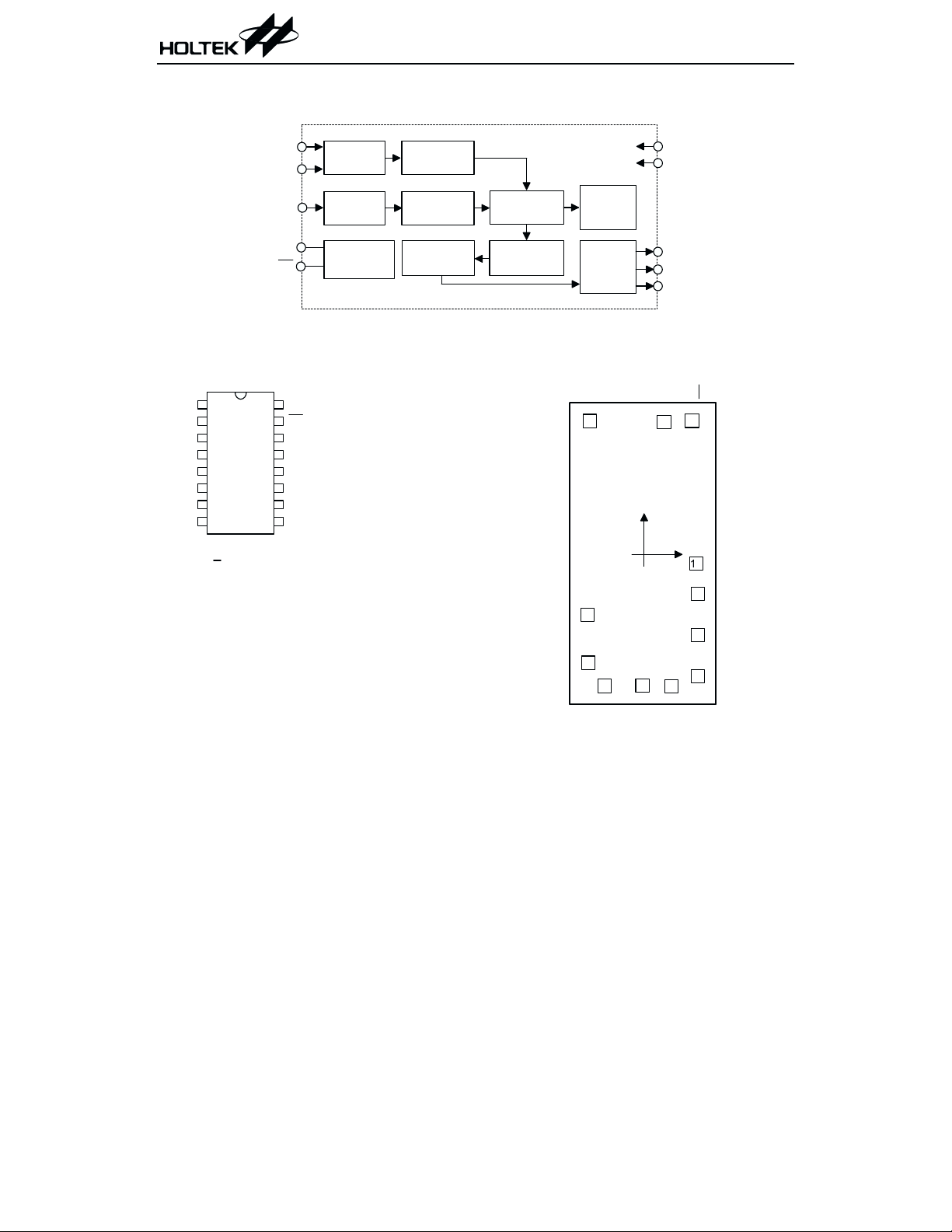
Block Diagram
Preliminary
HT81003/HT81R03
TG 1
I/O 1
OSCI
VPP
OE
D ebounce
Circuit
O s c illa to r
Circuit
OTP
Circuit
(for H T 81R03 only)
O ne-shot
Tim e Base
G enerator
Audio
C ontroller
ROM Address
C ounter
Data RO M
Status
Display
C ontroller
Selector
Pin Assignment Pad Assignment
NC
16 D IP
16
OE
15
VSS
14
OUT1
13
VDD
12
OUT2
11
VSS
10
I/O 2
9
VDD
OSCI
1
2
NC
VPP
NC
VDD
NC
OSCI
KEY1
I/O 1
1
2
3
4
5
6
7
8
HT81R03
(0 ,0 )
VDD
VSS
I/O 2
OUT1
OUT2
VPP
11
OE
12
10
VSS
9
OUT1
VDD
8
3
KEY1
4
5
I/O 2
I/O 1
Chip size: 1020 ´ 1995 (mm)
7
6
VSS
OUT2
2
* The IC substrate should be connected to VSS
in the PCB layout artwork.
2 July 24, 2000

Preliminary
HT81003/HT81R03
Pad Coordinates
Pad No. X Y Pad No. X Y
1
2
3
4
5
6 174.15
-345.85
-361.00 -385.35
-356.60 -691.45
-254.00 -839.95
-11.10 -838.55
850.70 7 343.85
8 343.85
9 343.85
10 334.25
11 305.30 851.65
-842.65
12 128.18 844.24
Unit: mm
-778.05
-514.85
-251.65
-58.75
Pin Description
Pin No. Pin Name I/O
1,3,5,16 NC
2 VPP
4, 12 VDD
6 OSCI I
7 KEY1 I Pull-high Trigger key 1, active low
8 I/O1 I
9 I/O2 O
10, 14 VSS
11 OUT2 O CMOS PWM output +/NMOS output
13 OUT1 O CMOS
15 OE
Internal
Connection
¾¾
¾¾
¾¾
¾
NMOS
Pull-high
NMOS
Pull-high
¾¾
¾¾
Description
No connection
Positive power supply
Oscillator input pin
Trigger key 2, active low/NMOS output
Pull-high/transistor output/NMOS output
Negative power supply
PWM output -/NMOS output
Absolute Maximum Ratings
Supply Voltage ................................-0.3V to 6V
Input Voltage ............... V
Note: These are stress ratings only. Stresses exceeding the range specified under ²Absolute Maxi
mum Ratings² may cause substantial damage to the device. Functional operation of this de
vice at other conditions beyond those listed in the specification is not implied and prolonged
exposure to extreme conditions may affect device reliability.
-0.3V to VDD+0.3V
SS
Storage Temperature ............... -50°Cto125°C
Operating Temperature .............-20°Cto70°C
3 July 24, 2000
-
-

Preliminary
HT81003/HT81R03
Electrical Characteristics
Symbol Parameter
V
I
I
I
I
I
I
I
V
V
DD
STB
OL1
OH1
OL2
OH2
OL3
Operating Voltage
DD
Operating Current 3V No load (OSC on)
Standby Current 3V
OUT1 (PWM+)
PWM Output Current
I/O2 (TR)
Tr Output Current
I/O1 (FLAG Sink Current) 3V
²H² Input Voltage ¾¾
IH
²L² Input Voltage ¾¾
IL
Test Conditions
V
DD
¾¾
3V
3V
3V
3V
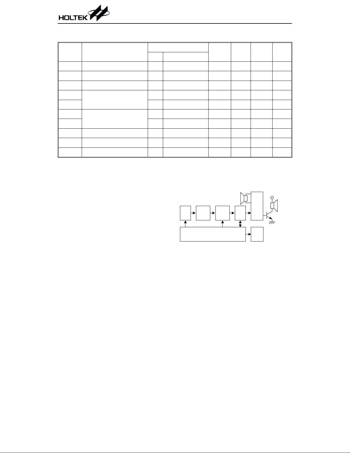
Functional Description
The EasyVoiceTMis voice synthesizer with
3-second voice capacity. A group of pre-recorded
voice sections is played upon receipt of key trigger
input signals. Two FLAG signals are output
while playing voices.
The 3-sec voice capacity can be divided into sections of arbitrary length. Notice that the silence
length and end-pulse width are not included in
the memory.
By using Holtek¢s programming tools, the contents and arrangement of sections, as well as
key features and FLAG output are all programmable before device fabrication.
The IC provides 2 key inputs (KEY1~KEY2),
KEY1 can be optioned as a direct, sequential
trigger key. Key 2 can be selected as a stop or a
direct key.
Conditions
¾¾
V
=0.1V
OL
V
OH
V
OL
V
OH
V
OL
=0.9V
=0.1V
=0.9V
=0.1V
DD
DD
DD
DD
DD
0.8V
Play function block diagram
Key
trigger
Key
features
option
Play control logic
Ta=25°C
Min. Typ. Max. Unit
2.4
¾
¾
1000 1200
13
75 90
36
13
-1 -2 ¾
35
¾
DD
0
Key
fu n c tio n
table
ROM
8/16/32
speaker
¾
W
Voice
ROM
3.6 V
¾
¾
¾
¾
V
DD
0.2V
DD
PW M +
PW M
-
Select
TR
Flag
output
mA
mA
mA
mA
mA
mA
mA
V
DD
speaker
V
V
8
W
4 July 24, 2000
 Loading...