8.4-Second LOG-PCM Speech
Features
Operating voltage: 2.4V~5.0V
·
Directly drives an external transistor
·
Low standby current (1mA typ. for VDD=3V)
·
Minimal external components
·
508 words table ROM for key functions
·
Programmable silence length and end-pulse
·
width (minimal end-pulse width is 330msata
6kHz sampling rate)
8.4-second voice capacity (based on a 6kHz
·
sampling rate)
12 keys
·
Controllable volume
·
FLAG1 options
·
-
End-pulse output
-
3HzB flash
-
6HzB flash
-
Voice output indication
-
Busy output
HT814D0
FLAG2 options
·
-
3Hz flash
-
6Hz flash
-
Busy output
Key options
·
-
Stop key: KEY12
-
Random (only for KEY1)
-
Sequential (only for KEY1)
-
Repeat (for all KEYs)
-
Key debounce time (for all KEYs): 700ms,
22ms, 45ms, 180ms (based on a sampling
rate of approximate 6kHz)
-
One shot (for all KEYs)
-
Level-trigger
-
Pull-high resistance (for all KEYs)
Section options
·
-
Retriggerable
-
Non-retriggerable
Dice form or 20/24-pin DIP/SOP package
·
Applications
Leisure products
·
Alarm clocks
·
Public address system
·
General Description
The HT814D0 is a single chip LOG-PCM voice
synthesizer LSI with 8.4-second voice capacity
at a 6kHz sampling rate. The chip when trig
gered drives a speaker through an external
transistor with a current switch D/A converter
output. Negligible current will be consumed in
the standby state.
The HT814D0 provides 12 key inputs and 2 pro
grammable FLAG outputs. With a 2.4V~5.0V
power supply, a complete synthesized voice
playback system can be easily built with very
few external components.
Alert and warning system
·
Sound effect generators
·
The customer¢s voice sources are recorded section by section into an internal mask ROM. The
-
sectional playback arrangement instructions of
each key are stored in the table ROM. The key
features are also programmable. With such a
flexible structure, the HT814D0 is excellent for
versatile voice applications.
-
1 March 15, 2000

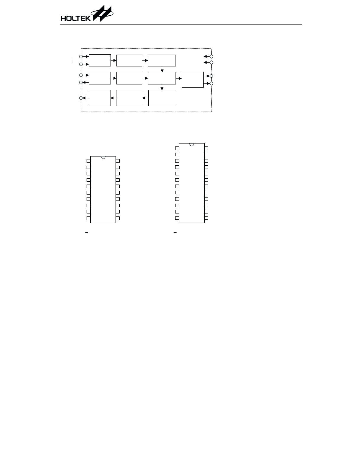
Block Diagram
HT814D0
KEY1
KEY12
OSC1
OSC2
AUD
D ebounce
Circuit
O s c illa to r
Circuit
DAC &
Output
C ontrol
Pin Assignment
KEY7
1
KEY8
2
KEY9
NC
VDD
AUD
OSC2
3
4
5
6
7
8
9
10
H T 8 1 4 D 0
20 D IP/SO P
KEY10
KEY11
KEY12
Speech R OM
20
19
18
17
16
15
14
13
12
11
O ne-shot
Tim e Base
G enerator
48K
6 -b it
´
KEY6
KEY5
KEY4
KEY3
KEY2
KEY1
FLAG 2
VSS
FLAG 1
OSC1
Key Table
Table R O M
508 ´ 14-bit
ROM
Address
Counter
KEY7
KEY8
KEY9
KEY10
KEY11
KEY12
NC
VDD
AUD
OSC2
OSC1
FLAG 1
S ta tu s
D isplay
C ontroller
1
2
3
4
5
6
7
8
9
10
11
12
24
23
22
21
20
19
18
17
16
15
14
13
H T 8 1 4 D 0
24 D IP/SO P
VDD
VSS
FLAG 1
FLAG 2
KEY6
KEY5
KEY4
KEY3
KEY2
KEY1
NC
NC
NC
NC
FLAG 2
VSS
2 March 15, 2000

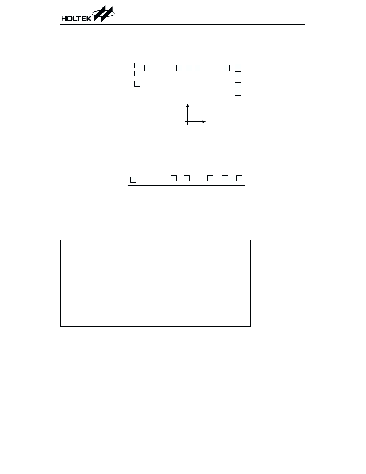
Pad Assignment
KEY9
KEY8
KEY7
KEY6
HT814D0
KEY5
* The IC substrate should be connected to VSS in the PCB layout artwork.
Pad Coordinates
KEY10
KEY11
KEY12
VDD
1
2
3
4
18 19
5 6
AUD
Chip size: 2270 ´ 2450 (mm)
17
OSC2
(0 ,0 )
14
15 16
8
7
FLAG 1
OSC1
2
KEY4
13
KEY3
12
KEY2
11
KEY1
10
9
FLAG 2
VSS
Unit: mm
Pad No. X Y Pad No. X Y
1
2
3
4
5
6
-914.500
-914.500
-914.500
-987.900 -1048.550
-254.600 -1022.050
-18.900 -1022.050
7 411.900
8 674.700
9 806.100
10 937.900
1023.050 11 912.800 526.250
879.650 12 912.800 664.850
689.050 13 912.800 860.250
14 912.800 1003.850
15 709.500 974.350
16 179.200 974.350
-1022.050
-1022.050
-1052.650
17 22.000 974.350
18
19
-156.400
-734.200
974.350
974.350
-1022.050
3 March 15, 2000

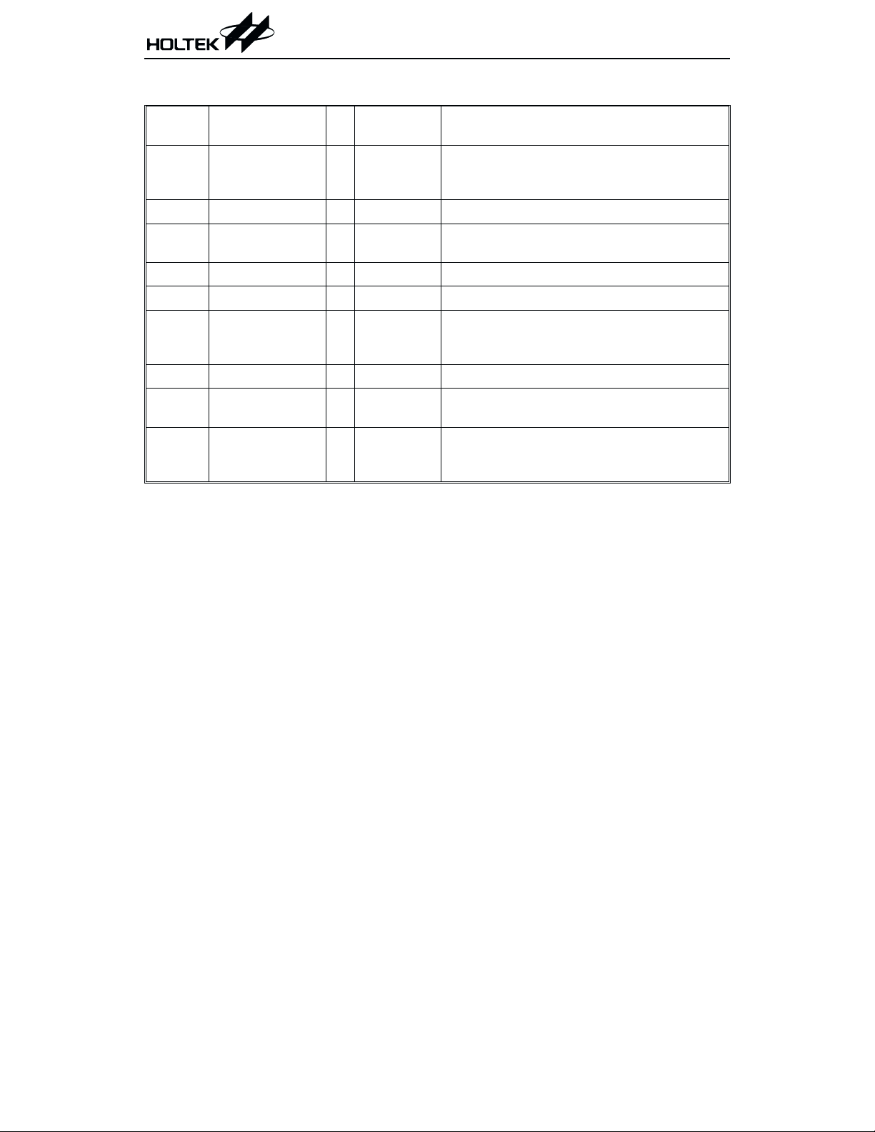
Pad Description
HT814D0
Pad No. Pad Name I/O
1~3 KEY10~KEY12 I Pull-high
4 VDD
5 AUD O
6 OSC2 O
7 OSC1 I
8 FLAG1 O
9 VSS
10 FLAG2 O
11~19 KEY1~KEY9 I Pull-high
Internal
Connection
¾¾
PMOS
Open Drain
¾
¾
NMOS
Open Drain
¾¾
NMOS
Open Drain
Absolute Maximum Ratings
Description
Trigger key, active low. Key features such as
debounce time, pull-high resistance and repeat
(by mask option)
Positive power supply
Voice output for driving an external transistor
Oscillator output pin
Oscillator input pin
3HzB/6HzB flash output, busy output,
end-pulse or voice output indication (by mask
option). Open drain, active low output.
Negative power supply, ground
3Hz/6Hz flash output or busy output (by mask
option). Open drain, active low output.
Trigger key, active low. Key features such as
debounce time, pull-high resistance and repeat
(by mask option)
Supply Voltage ................................-0.3V to 6V
Input Voltage ............... V
Note: These are stress ratings only. Stresses exceeding the range specified under ²Absolute Maxi-
mum Ratings² may cause substantial damage to the device. Functional operation of this device
at other conditions beyond those listed in the specification is not implied and prolonged exposure to extreme conditions may affect device reliability.
-0.3V to VDD+0.3V
SS
Storage Temperature ................-50°Cto125°C
Operating Temperature .............-20°Cto70°C
4 March 15, 2000

HT814D0
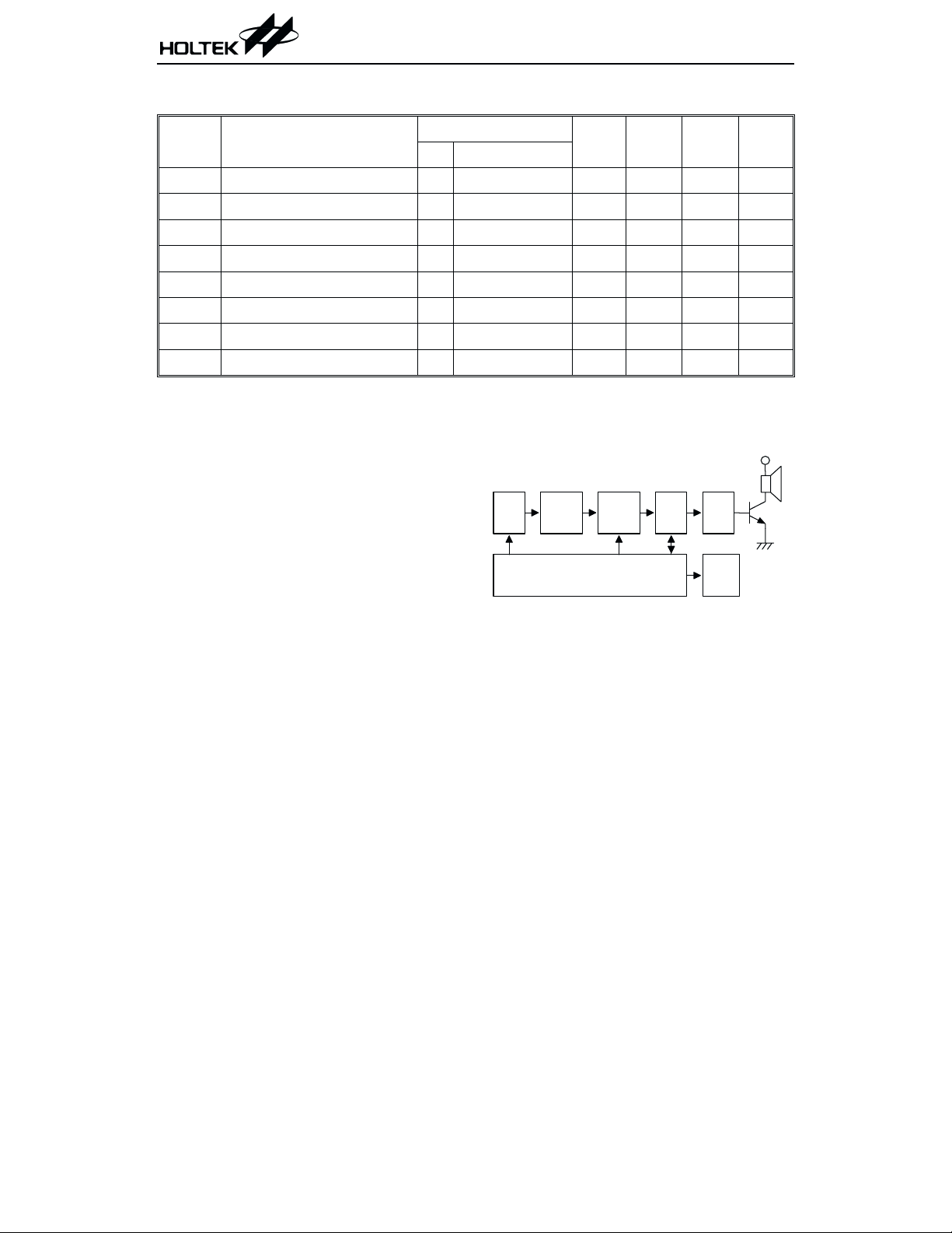
Electrical Characteristics
Symbol Parameter
V
I
DD
I
STB
I
O
I
OL
V
V
f
OSC
DD
IH
IL
Operating Voltage
Operating Current 3V No load
Standby Current 3V
Max. AUD Output Current 3V
FLAG Sink Current 3V
²H² Input Voltage ¾¾
²L² Input Voltage ¾¾
Oscillating Frequency 3V
Test Conditions
V
DD
¾¾
Functional Description
The HT814D0 is a mask ROM type voice synthe
sizer with 8.4-second voice capacity. A group of
pre-recorded voice sections is played upon receipt
of key trigger input signals. Two FLAG outputs
send signals are while playing voices.
The 8.4-second voice capacity can be divided into
sections of arbitrary length. Notice that the silence length and end-pulse width are not included in the memory.
By using Holtek¢s programming tools, the contents and arrangement of sections, as well as
key features and FLAG output are all programmable before device fabrication.
The IC provides 12 key inputs (KEY1~KEY12).
Of the 12 keys, KEY1 can be optioned as a direct, sequential or random trigger key. KEY12
can be selected as a stop or direct key. The re
maining 10 keys (KEY2~KEY11) are used as di
rect keys exclusively.
Conditions
Min. Typ. Max. Unit
2.4
¾¾
V
=0.6V
OH
=0.3V
V
OL
-1.5 -2 ¾
1.5 3.0
0.8V
=530kW
R
OSC
Play function block diagram
-
Key
trigger
Key
features
option
Play control logic
¾
¾
200 400
13
¾
DD
0
¾
76 96 116 kHz
Key
function
table
ROM
Voice
ROM
5.0 V
¾
V
0.2V
System oscillator
The HT814D0 has a built-in RC oscillator
which requires only one external resistor for
normal applications. The oscillator frequency is
typically 96kHz for an external resistor of
530kW. The required oscillator frequency may
vary with different sampling rates in the process
of voice programming. As a result, the values of
the oscillator resistor may be different for different
items.
DD
DD
D/A
Flag
output
Ta=25°C
mA
mA
mA
mA
V
V
V
DD
5 March 15, 2000
