

CMOS Switched-Capacitor Voltage Converter
Features
Simple conversion of VDDto -V
·
Cascade connection (two devices are
·
connected, V
Boost pin for higher switching frequency
·
Easy to use
·
-
Requires only two external capacitors
= -2VDD)
OUT
Applications
RS-232 power supply
·
On board negative supply for dynamic
·
RAMS
Supply voltage splitter, VO= ± VDD/2
·
General Description
HT7660 is a monolithic CMOS switched-capacitor voltage converter. HT7660 is designed to
complete a voltage conversion from positive to
negative. The only required external compo
nents aretwo low cost electrolytic capacitors.
HT7660 includes a voltage regulator, an RC oscillator and four output power MOS switches.
DD
HT7660
No external diode required
·
Typically with no load voltage conversion,
·
99.9% efficiency
Typical power efficiency is 98%
·
Wide operating voltage range: 3V to 12V
·
Operation amplifier supply
·
Data acquisition systems
·
Positive voltage doubler
·
The frequency of an RC oscillator can be low
ered by adding an external capacitor between
V
and the OSC pin, or an external clock can
DD
be connected to the OSC pin to replace the origi
nal oscillator. The LV terminal may be tied to
VSS to disable the voltage regulator. By doing
this, low voltage operation can be improved.
-
-
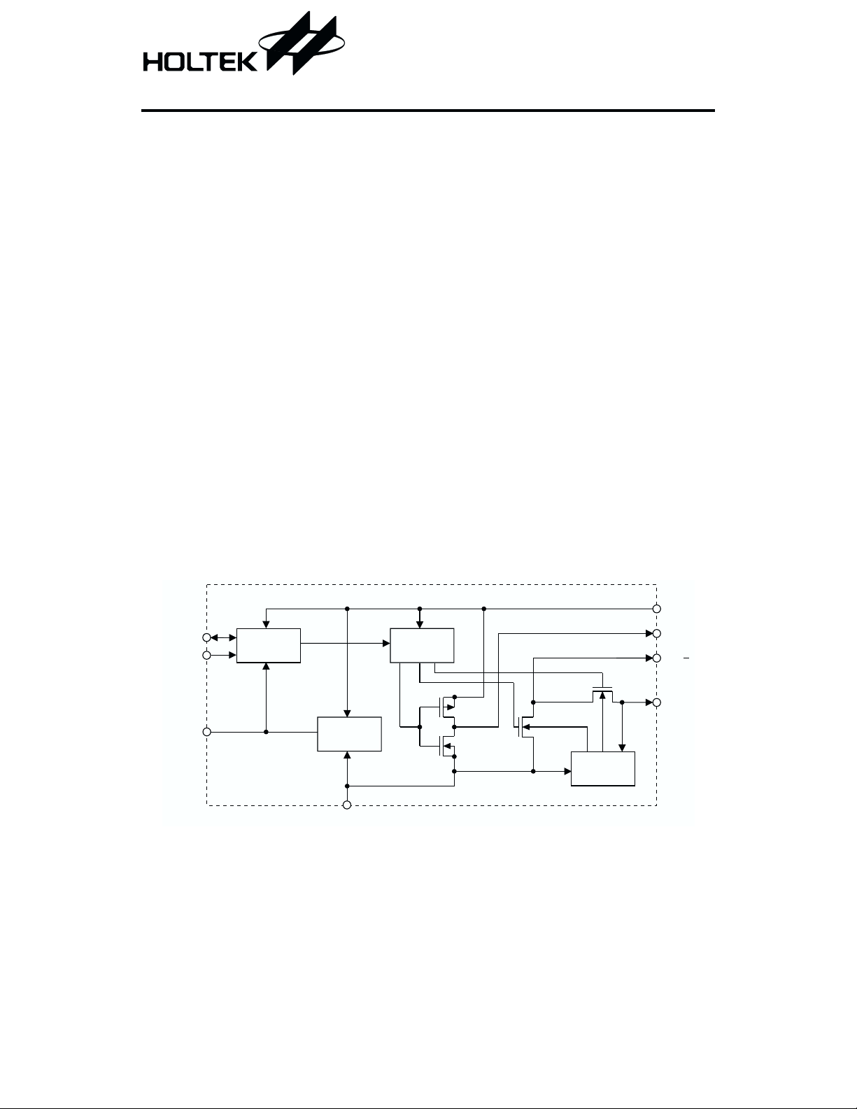
Block Diagram
OSC
BOOST
LV
RC
Oscillator
Voltage
Regulator
VSS
Voltage
Level Shifter
Logic
Network
1 November 30, 1999
VDD
CAP+
CAP
VOUT
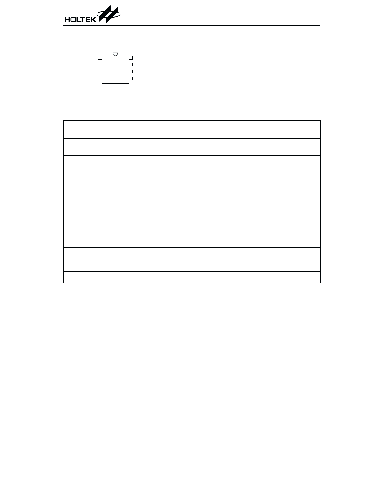
Pin Assignment
HT7660
BOOST
CAP+
VSS
CAP
1
2
3
-
4
VDD
8
OSC
7
LV
6
VOUT
5
H T 7 6 6 0
8 DIP/SOP
Pin Description
Pin No. Pin Name I/O
1 BOOST I
2 CAP+ O CMOS
3 VSS
4
CAP-
5 VOUT O NMOS
6LV I
7 OSC I/O
8 VDD
¾¾
O NMOS
¾¾
Internal
Connection
CMOS
Pull-low
¾
Transmission
Gate
Description
Higher switching frequency selection input
This pin is connected to the positive terminal of Ca
pacitor C1 for a charge pump
Negative power supply, ground
This pin is connected to the negative terminal of Ca
pacitor C1 for a charge pump
This pin is connected to the negative terminal of Ca
pacitor C2 for charge reservoir. Output voltage pass
through this pin
Floating this pin enables the voltage regulator. Connect this pin to VSS (Ground) to bypass voltage regulator and improve low voltage operation
External clock input pin. This pin can be connected
with an external capacitor to reduce switching frequency
Positive power supply
-
-
-
2 November 30, 1999
Absolute Maximum Ratings
HT7660
Supply Voltage ..............................-0.3V to 13V
Operating Temperature ..............-40°Cto85°C
Storage Temperature.................-50°Cto125°C
Note: These are stress ratings only. Stresses exceeding the range specified under ²Absolute Maxi
mum Ratings² may cause substantial damage to the device. Functional operation of this device
at other conditions beyond those listed in the specification is not implied and prolonged expo
sure to extreme conditions may affect device reliability.
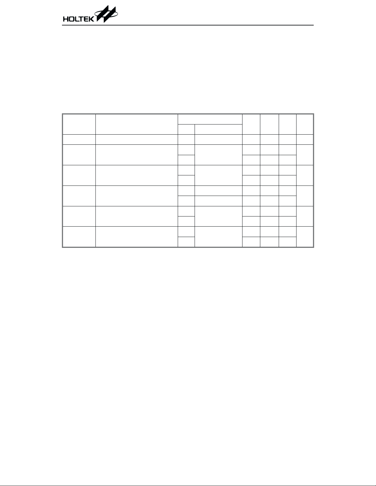
Electrical Characteristics
Ta=25°C
Test Conditions
Symbol Parameter
V
DD
I
STB
f
OSC
R
OUT
V
CON-EFF
P
EFF
Operating Voltage
Standby Current
System Frequency
Output Source Resistance
Voltage Conversion Efficiency
Power Efficiency
DD
Conditions
V
¾¾
3V
No load
5V
3V
¾
5V 5 10
I
OUT
I
OUT
=10mA
=20mA
3V
5V
3V
No load
5V 99 99.9
3V
5V 96 98
5kW
R
L=
Min. Typ. Max. Unit
3
¾
12 V
¾
26 100
mA
80 160
¾
2.5 4
¾
kHz
¾
97 150
¾
W
60 100
¾
99
¾¾
%
¾
96
¾¾
%
¾
-
-
3 November 30, 1999

Functional Description
HT7660 needs only two external polarized elec
trolytic capacitors to complete a negative volt
age converter.
HT7660 has four MOS power switches: S1, S2,
S3 and S4. For the first half cycle, when S2 and
S4 are open, Capacitor C1 is charged to a volt
age V
half cycle, when S1 and S3 are open, the charge
on Capacitor C1 is shifted to Capacitor C2
through S2 and S4. Thereby, the voltage across
Capacitor C2 is V
minal of C2 is connected to V
voltage at V
through S1 and S3. During the second
DD
. Because the positive ter
OUT
DD
pin.
, we get a -V
SS
DD
For high voltage operation, the LV pin is left
floating to enable the voltage regulator. This
can reduce the current consumption of the RC
oscillator, and thus get a fixed switching fre
quency Fosc with high voltage range. For low
voltage operation, the LV pin is connected to
V
to bypass the voltage regulator of which in
SS
herent voltage drop can degrade the operation
at low voltages.
A capacitor may be connected between V
pin OSC to lower the switching Fosc, and an ex
ternal clock may be added to replace the
built-in RC oscillator.
HT7660
and
DD
-
-
-
V
DD
V
SS
S1
S3
CAP+
C1
CAP
S2
V
SS
C2
S4
-
V
= -V
OUT
DD
The operating mode of HT7660
4 November 30, 1999

Application Circuits
Simple negative voltage converter
HT7660
Simple voltage multiplier
2
CAP+
10mF
4
CAP
3
VSS
V
10mF
-
H T 7660
DD
VDD
VOUT
1
2
4
3
BOOST
CAP+
CAP
VSS
8
5
-
H T 7660
V
DD
10mF
VDD
LV
VOUT
V
DD
8
6
5
= -V
V
OUT
DD
10mF
8
2
4
3
CAP+
CAP
VSS
VDD
VOUT
5
10mF
= -2V
V
OUT
DD
-
H T 7660
10mF
5 November 30, 1999

External switching frequency
10mF
Lower switching frequency
10mF
2
4
3
CAP+
CAP
VSS
2
4
3
-
H T 7660
CAP+
CAP
-
VSS
VDD
OSC
VDD
OSC
HT7660
V
DD
8
1k
7
5
8
7
5
V
DD
W
CMOS
Gate
V
OUTVOUT
10mF
V
DD
C
OSC
V
OUTVOUT
10mF
H T 7660
N ote: C OSC is te n s o f p ic o fa ra d
6 November 30, 1999

Positive voltage doubler
2
3
CAP+
VSS
VDD
VOUT
HT7660
V
DD
8
D1
5
D2
V
= 2V
OUT
DD -2VD
Voltage splitter
H T 7660
10mF10mF
N ote: V D is forw ard voltage drop of diode D1 and D 2
R
L1
47mF
47mF
2
4
3
CAP+
CAP
VSS
-
H T 7660
V
V
DD
EE
R
OUT
L2
-
=
2
V
47mF
VDD
LV
VOUT
8
6
5
V
DD
V
EE
7 November 30, 1999

Combined negative voltage converter and positive voltage doubler
V
DD
8
VDD
D1
-
VOUT
5
10mF
4
2
3
CAP+
CAP
VSS
10mF
HT7660
V
= -V
OUT
DD
H T 7660
10mF
D2
10mF
N ote: V D is forw ard voltage drop of diode D1 and D 2
V
OUT
= 2VDD -2V
D
8 November 30, 1999

HT7660
Holtek Semiconductor Inc. (Headquarters)
No.3 Creation Rd. II, Science-based Industrial Park, Hsinchu, Taiwan, R.O.C.
Tel: 886-3-563-1999
Fax: 886-3-563-1189
Holtek Semiconductor Inc. (Taipei Office)
5F, No.576, Sec.7 Chung Hsiao E. Rd., Taipei, Taiwan, R.O.C.
Tel: 886-2-2782-9635
Fax: 886-2-2782-9636
Fax: 886-2-2782-7128 (International sales hotline)
Holtek Semiconductor (Hong Kong) Ltd.
RM.711, Tower 2, Cheung Sha Wan Plaza, 833 Cheung Sha Wan Rd., Kowloon, Hong Kong
Tel: 852-2-745-8288
Fax: 852-2-742-8657
Copyright Ó 1999 by HOLTEK SEMICONDUCTOR INC.
The information appearing in this Data Sheet is believed to be accurate at the time of publication. However, Holtek
assumes no responsibility arising from the use of the specifications described. The applications mentioned hereinare
used solely for the purpose of illustration and Holtek makes no warranty or representation that such applications
will be suitable without further modification, nor recommends the use of its products for application that may pres
ent a risk to human life due to malfunction or otherwise. Holtek reserves the right to alter its products without prior
notification. For the most up-to-date information, please visit our web site at http://www.holtek.com.tw.
9 November 30, 1999
-
 Loading...