


General Purpose PIR Controller
Features
•
Stand-by current: 100µA (Typ.)
•
On-chip regulator
•
Adjustable output duration
•
CDS input
•
40 second warm-up
•
ON/AUTO/OFF selectable by MODE pin
Applic ations
•
PIR light controllers
•
Motion detectors
General Description
The HT761X is a CMOS LSI chip designed for
use in automatic PIR lamp control. It can operate with a 2-wire configuration for tr iac applications or with a 3-wire configuration for relay
applications. The chip is equipped with operational amplifiers, a comparator, timer, a zero
crossing detector, control circ uit, a voltage r egulator, a system oscillator, and an output timing
oscillator.
Its PIR sensor detects infrared power variations induced by the motion of a huma n body
and transforms it to a volta ge variation. If the
HT761X
•
Override function
•
Auto-reset if the ZC signal disappears over
3 seconds
•
Operating voltage: 5V~12V
•
16 pin DIP or SOP packaging
•
Alarm systems
•
Auto door bells
PIR output voltage variation conforms to the
criteria (refer to the functional description), the
lamp is turned on with an adjustable duration.
The HT761X offers three operating modes (ON,
AUTO, OFF) which can be set through the
MODE pin. While the chip is working in the
AUTO mode the user can ov erride it and s witch
to the TEST mode, or manual ON mode, or
return to the AUTO mode by switching the
power switch. The chip is enclosed in a 16 pin
DIP/SOP.
Selection Table
Part Number
HT7610 2 times Flash 8 hrs
HT7611 1 time No flash 8 hrs
ZC off/on for
override
Flash on
mode auto-
change
1 24th Mar ’97
Override ON
duration
Comparator
window
1
(VDD-VEE)
16
1
(VDD-VEE)
16
Effective
trigger width
>24ms
>24ms
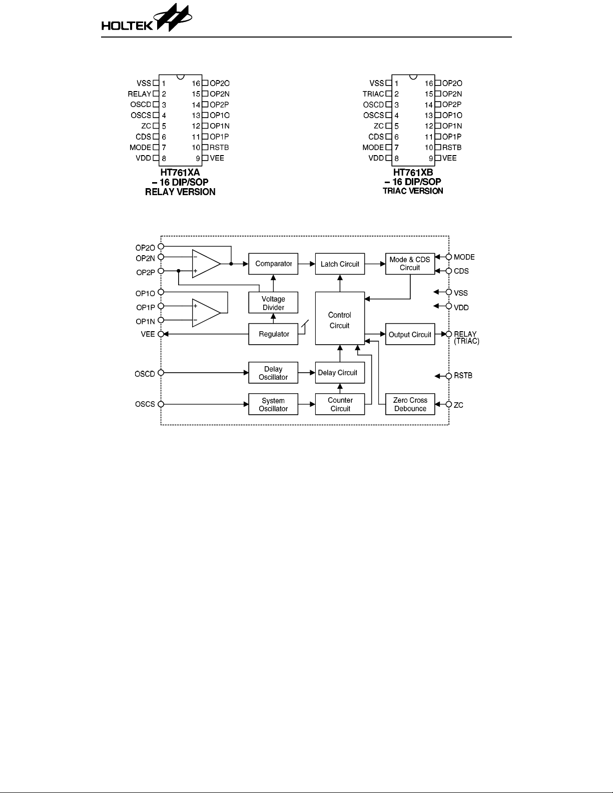
Pin Assignment
Block Diagram
HT761X
2 24th Mar ’97

Pin Description
HT761X
Pin No.
Pin Name I/O
AB
1 1 VSS I — Negative power supply
2 RELAY O CMOS
2 TRIAC O CMOS
3 3 OSCD I/O
4 4 OSCS I/O
5 5 ZC I CMOS Input for AC zero crossing detection
6 6 CDS I CMOS
7 7 MODE I CMOS
8 8 VDD I — Positive power supply
9 9 VEE O NMOS
10 10 RSTB I Pu ll-High Chip reset input, active low
11 11 OP1P I PMOS Noninverting input of OP1
12 12 OP1N I PMOS Inverting input of OP1
13 13 OP1O O NMOS Output of OP1
14 14 OP2P I PMOS Noninverting input of OP2
15 15 OP2N I PMOS Inverting input of OP2
16 16 OP2O O NMOS Output of OP2
Internal
Connection
PMOS IN
NMOS OUT
PMOS IN
NMOS OUT
Description
RELAY drive output through an external NPN
transistor, active high
TRIAC drive output
The output is a pulse output when active.
Output timing oscillator I/O
It is connected to an externa l RC to adjust outpu t
duration.
System oscillator I/O
OSCS is connected to an external RC to set the
system frequency. The system frequency
for normal application.
CDS is connected to a CDS voltage divider for
daytime/night auto-detection. Low input to this pin
can disable the PIR input. CDS a schmitt trigger
input with 5-second input debounce time.
Operating mode selection input:
VDD: Output is always ON
VSS: Output is always OFF
Open: Auto detection
Regulated voltage o utput
The output voltage is about –4V with respect to
VDD.
≅ 16KHz
3 24th Mar ’97

HT761X
Absolu te Maximum Ra tin g s
Supply Voltage...............................–0.3V to 13V Operating Temperature...............–25°C to 75°C
Input Voltage................. V
Storage Temperature.................–50
Electrical Characteristics
–0.3V to VDD+0.3V Zero Crossing Current.....................max. 300µA
SS
°C to 125°C
Symbol Parameter
V
V
I
DD
V
V
I
OH1
I
OL1
I
OL2
V
V
V
V
F
F
A
V
Operating Voltage — — 5 9 12 V
DD
Regulator Output Voltage 12V VDD–V
EE
Operating Current 12V No load, OSC on — 100 350 µA
CDS “H” Transfer Voltage 12V — 6.4 8 9.6 V
TH1
CDS “L” Transfer Voltage 12V — 3.7 4.7 5.6 V
TL1
OUTPUT Source Current
(RELAY, TRIAC)
OUTPUT Sink Current
(RELAY, TRIAC)
VEE Sink Current 12V VDD–VEE=4V — 1 — mA
“H” Input Voltage — — 0.8V
IH
“L” Input Voltage — — — — 0.2V
IL
ZC “H” Transfer Voltage 12V — 4.7 6.7 8.7 V
TH2
ZC “L” Transfer Voltage 12V — 1.3 1.8 2.3 V
TL2
System Oscillator Frequency 12V
SYS
Delay Oscillator Frequency 12V
d
OP Amp Open Loop Gain 12V No load 60 80 — dB
VO
OP Amp Input Offset Voltage 12V No load — 10 35 mV
OS
Test Condition
V
DD
12V V
12V V
Condition
=10.8V –6 –12 — mA
OH
=1.2V 40 80 — mA
OL
R
OSCS
C
OSCS
R
OSCD
C
OSCD
EE
=560K
=100P
=560K
=100P
Min. Typ. Max. Unit
3.5 4 4.5 V
——V
DD
V
DD
12.8 16 19.2 KHz
12.8 16 19.2 KHz
4 24th Mar ’97

Trigger Timing
HT761X
Note: 1. The output is activated if the trigger signal conforms to the following criteria:
• More then 3 triggers within 2 seconds.
• A trigger signal sustain duration ≥ 0.34 secs.
• 2 trigger signals within 2 secs with one of the trigger signal sustain ≥ 0.16 secs.
2. The effective comparator output width can be selected to be 24ms or 32ms or
48ms by mask option. The default is 24ms (system frequency=16KHz).
3. The output duration is set by an external RC that is connected to the OSCD pin.
5 24th Mar ’97

Functional Description
HT761X
VEE
VEE supplies power to the analog front end
circuit with a sta bilized voltage which is –4V
with respect to VDD normally.
OSCS
OSCS is a system oscillator input pin. When it
is connected to an external RC a system frequency of 16KHz can be generated.
Fig.1 System osc illator
OSCD
OSCD is an output timing oscillator input pin.
It’s connected to an e xternal RC to obtain the
desired outp ut turn-on durati on. Variable output turn-on durations can be achieved by selecting various values of RC or using a variable
resistor.
RELAY (TRIAC)
RELAY is an output pin set as a RELAY driving
(active high) output for the HT761XA, or as a
TRIAC driving (active low) output for the
HT761XB.
The output acti ve du ration is con trolle d by the
OSCD oscillating period.
HT761XA HT761XB
OUTPUT RELAY TRIAC
CDS
CDS is a CMOS schmitt trigger input structure.
It is used to distinguish betwe en day time and
night time. When the input voltage of CDS is
high the PIR input is enabled. On the other
hand, when CDS is low the PIR input is disabled. The input disable to enable debounce
time is 5 seconds. Connect this pin to VDD
when not using this function. The CDS input is
ignored when the output is active.
CDS Status PIR
LOW Day Time Disabled
HIGH Night Enabled
1
TD=
× 21504
f
Fig.2 Output timi ng oscillator
6 24th Mar ’97

HT761X
MODE
MODE is a tri-state input pin used to select the
operating mo de.
MODE
Status
VDD ON
Open AUTO
Operating
Mode
VSS OFF
Description
Output is always ON:
RELAY outputs high for
relay driving.
TRIAC pulse train output
is synchronized by ZC for
triac driving.
Output is always OFF:
RELAY outputs low for
relay driving.
TRIAC outp uts high for
triac driving.
Outputs remain in the off
state until activated by a
valid PIR input trigger
signal. When working in
the AUTO mode, the chip
allows override control by
switching the ZC signal.
ZC
ZC is a CMOS inpu t structure. It receives AC
line frequency and generates zero crossing
pulses to synchronize the triac drive r. By effective ZC signal switching (switch OFF/ON 1 or 2
times within 3 seconds by mask option), the
chip provides the following additional functions:
•
Test mode control
Within 10 seconds after power-on, effective
ZC switching will force the chip to enter the
test mode. During the tes t m ode , the o utputs
will be active for a duration of 2 seconds each
time a valid PIR trigger s ignal is received. If
a time interval exceed s 32 secon ds without a
valid trigger input, the chip will enter the
AUTO mode automatically.
7 24th Mar ’97

HT761X
•
Override control
When the chip is workin g in the AU T O mo d e
(MODE=open), the output is activated by a
valid PIR trigger signal and the output active
duration is controlled by the OSCD oscillating
period. The lam p can be switched always to
“ON” from the AUTO mo de by either switching the MODE pin to VDD or switching the ZC
signal by an OFF/ON operati on of the power
switch (OFF/ON once or twice withi n 3 seconds by mask option). The term "override"
refers to the change of operating mode by
switching the powe r switch. The chip can be
toggled from ON to AUT O by an ove rride o peration. If the ch ip is overridden to ON and
Fig.3 ZC override timing
RSTB
RSTB is use d to reset the chip. It is inte rnal
pull-high and active lo w.
The use of C
can extend the power-on initial
RST
time. If the RSTB pin is an open circuit (without
C
), the initial time is the default (40 secs).
RST
Fig.4 RSTB application ex am ple
there is no further ove rride operati on, it will
return to AUTO automatically after an internal preset ON time duration has elapsed. This
override ON time duration can be set to 4 or 6
or 8 hours by mask option. The default is 8
hours.
The chip provides a mask opt ion to d ecide t he
output flash times (3 times) when changing
the operating mode. It wi ll fla sh 3 time s at a
1Hz rate each time the chip changes from the
AUTO mode to anoth er m ode or f l a sh 3 t im es
at a 2Hz rate when re turning to the AUTO
mode. But if the AUTO mode is changed by
switching the MODE switch it will not flash.
Power on initial
The PIR signal amplifier requires a warm up
period after power-on. The input should be disabled during this period.
In the AUTO mod e within the first 10 seconds
of power-on initialization, the chip allows override control to enter the test mode. After 40
seconds of the initial time the chip allows override control between ON and AUTO. It will
remain in the warm up period if the total initial
time has not elapsed after returning to AUTO.
In case that the ZC signal disappears more than
3 seconds, the chip will restart the initialization
operation. However, the restart initial time is
always 40 seconds an d cannot be extended by
adding C
to the RSTB pin as shown in Fig.4.
RST
8 24th Mar ’97

Mask opt ions
The HT761X offers mask o ptions to select the
output flash (3 times) when changing the operating mode. The chip will flash 3 times at a 1Hz
rate each time it changes from AUTO to another
mode and flash 3 times at a 2Hz rate when it
returns to the AUTO mode . However the chip
will not flash if the mode is changed by switching the MODE switch.
•
4, 6, or 8 hour options to return to AUTO from
override ON. The default is 8 hours.
•
Options for effective override : Once or twice
OFF/ON operation of power switch within 3
seconds. The default is OFF/ON twice.
•
Options for outp ut flash to indicate effective
override operation. The default is to flash.
•
Options for effective PIR trigger pulse width:
>24mS, >32mS or >48mS. The default is 24ms.
•
Options for setting compa rator window to be
1
1
,
16
11.3
1
(VDD–VEE).
16
PIR amplifier
1
or
(VDD–VEE). The default is
9
Consult the diagram below for details on the
PIR front end amplifier.
In Fig.5 there are 2 op-amps with different
applications. OP1 can be used independently as
a first stage inve rting or non-invertin g amplifier for the PIR.
As the output of OP2 is directly connected to the
input of the comparato r, it is used as a second
HT761X
Fig. 5 PIR amplifier
stage amplifying de vice. The non-inverti ng input of OP2 is connected to the comparator’s
window centerpoint and can be used to check
this voltage and to provide a bias voltage that is
equal to the c enterpoi nt volt age of th e compar ator . In Fig.5 the comparator can have 3 window
levels set by mask option. 1.
1
(VDD–VEE), 3.
11.3
1
9
dow level fails to be s pecified the default window is set to
1
(VDD–VEE). The preset voltage
16
of VDD–VEE is 4 V. The default values of V
and VCN are therefore 0.25V, (
1
(VDD–VEE), 2.
16
(VDD–VEE). If the win-
CP
16
4
V ).
9 24th Mar ’97

Second stage amplif i e r
HT761X
Fig.6 Typical second stage amplifier
Usually the second stage PIR amplifier is a
simple capacitively coupled inve rting amplifier
with a low pass configuration. The noninverting
input terminal is biased to the cen ter point of
the comparator win dow and the output of the
second stage amplifier is directly coupled to the
comparator center point.
In Fig.6 OP2P is directly connected to the comparator window center, and with the C3 filter it
can act as the bias for OP2. For this configura-
tion A
R2
=
, low cutoff frequency fL =
V
R1
high cutoff frequency f
1
=
H
πR2C2
2
1
πR1C1
2
. By chang-
ing the value of R2 the sensitivity can be varied.
C1 and C3 should be of low leakage types to
prevent the DC operating point from change
due to current leakage.
Each op-amp curren t consumption is approximately 5
µA with the op-amps and comparator’s
working voltage all provided by the regulator.
Consult the following dia grams for typ ical P IR
front end circuit.
First stage of PIR amplifier
Fig.7 shows a typical first stage amplifier. C2
and R2 form a simple low pass filter with cut off
frequency at 7Hz. The low frequency response
is governed by R1 and C1 with cut-off frequency
at 0.33Hz.
( R1+ R2 )
A
=
V
R1
Fig.7 and Fig.8 are similar but in Fig.8 the
input signal of amplifier is taken from the drain
of the PIR. Thi s has higher gain than th at in
Fig.7. Since OP1 is a PMOS input V
greater than 1.2V for adequate operation.
,
Fig. 7 Typical first-stage PIR
Fig.8 High gain first stage
has to be
D
10 24th Mar ’97

Application Circuit
HT761XA relay application
HT761X
Note: 1. Adjust R13 to fit various CDS.
2. Change C6 to obtain the desired adjusting range of output duration.
3. Change the value of C11 to 0.33
µF/600V for AC 220V application.
11 24th Mar ’97

HT761XB triac application
HT761X
Note: 1. Adjust R10 to fit various CDS.
2. Change C7 to obtain the desired adjusting range of output duration.
3. Change the value of C10 to 0.15
µF/600V for AC 220V application.
12 24th Mar ’97
 Loading...