

Features
Low power consumption
·
Low temperature coefficient
·
Built-in high-stability reference source
·
Applications
Battery checkers
·
Level selectors
·
Power failure detectors
·
General Description
The HT70XX series is a set of three-terminal
low power voltage detectors implemented in
CMOS technology. Each voltage detector in the
series detects a particular fixed voltage ranging
from 2.4V to 7V. The voltage detectors consist of
a high-precision and low power consumption
standard voltage source, a comparator, hyster
HT70XX
Voltage Detector
Built-in hysteresis characteristic
·
TO-92 & SOT-89 package
·
Microcomputer reset
·
Battery memory backup
·
Non-volatile RAM signal storage protectors
·
esis circuit, and an output driver. CMOS tech
nology ensures low power consumption.
Although designed primarily as fixed voltage
detectors, these devices can be used with exter
nal components to detect user specified thresh
old voltages (NMOS open drain type only).
-
-
-
-
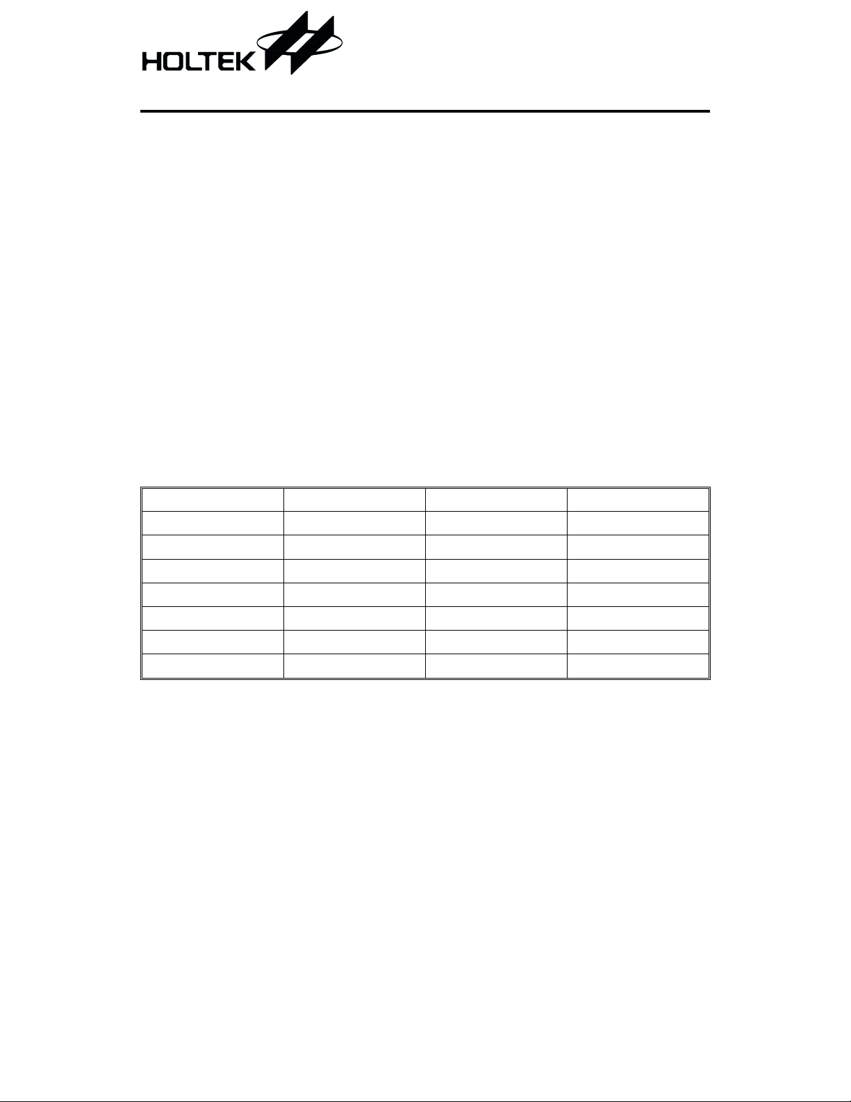
Selection Table
Part No. Detectable Voltage Hysteresis Width Tolerance
HT7024A
HT7027A
HT7033A
HT7039A
HT7044A
HT7050A
HT7070A
Note: The output type selection codes are:
NMOS open drain normal open, active low
PMOS open drain normal open, active high
For example: The HT7070A is a 7V, NMOS open drain active low output
2.4V 0.12V
2.7V 0.135V
3.3V 0.165V
3.9V 0.195V
4.4V 0.22V
5V 0.25V
7V 0.35V
1 May 3, 2000
±5%
±5%
±5%
±5%
±5%
±5%
±5%
Output type selection table
V
Type V
DD
OUT
VDD>V
DET
A Hi-Z VSS
Block Diagram
N channel open drain output (normal open; active low)
(+) VDD£V
DET
(-)
HT70XX
A type
VDD
GND
VOUT
V
REF
V
OUT
V
DET
V
HYS
V
IN
2 May 3, 2000
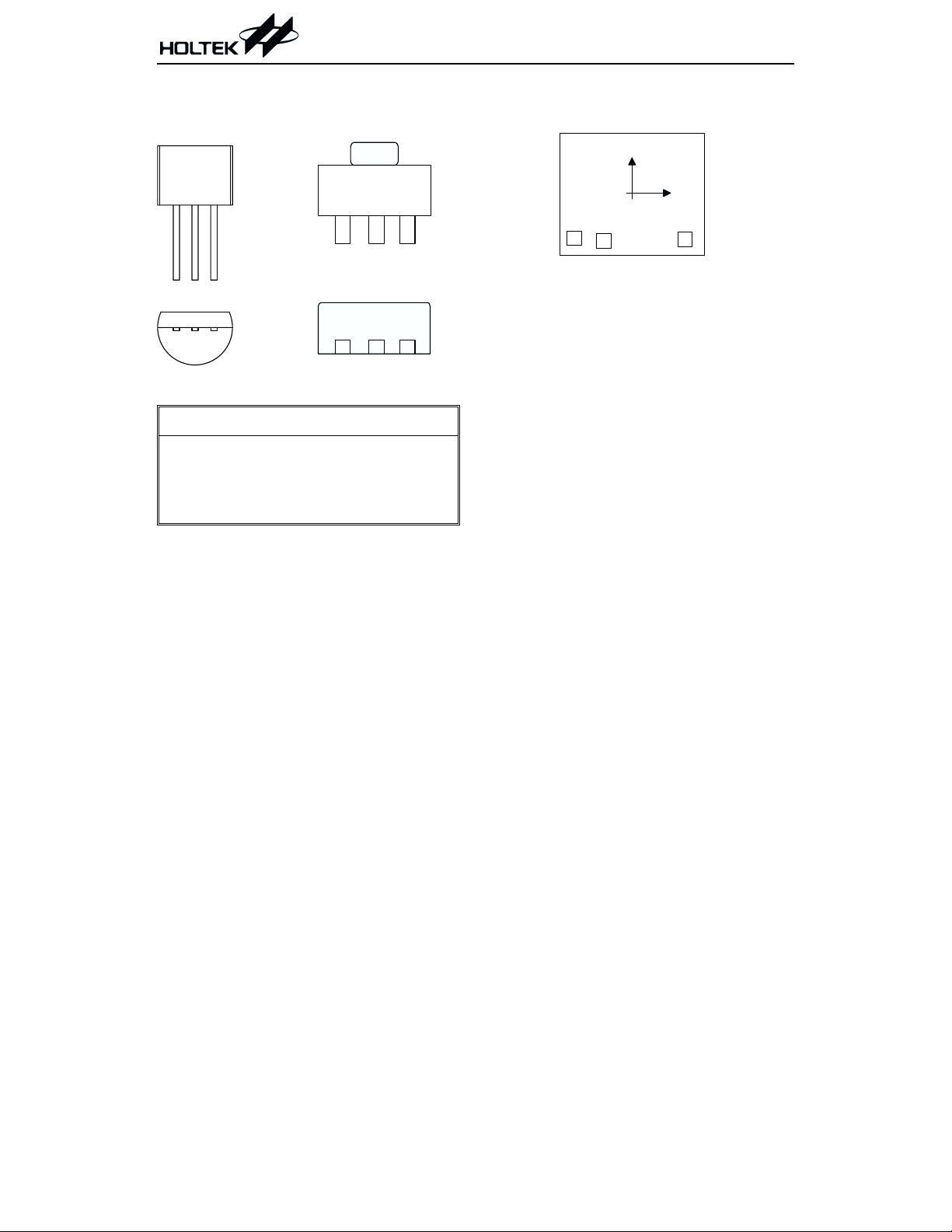
Pin Assignment Pad Assignment
HT70XX
TO -92
HT70XX
OUTVDD VSS
Front V iew
B o tto m V ie w
SO T-89
OUT VDD VSS
Pad Coordinates
Pad No. X Y
1
2
-483.30 -379.50
-234.60 -399.50
3 443.90
Absolute Maximum Ratings
Unit: mm
-386.00
(0 ,0 )
1
2
VOUT
VIN
Chip size: 1317 ´ 1158 (mm)
3
GND
2
* The IC substrate should be connected to VDD in
the PCB layout artwork.
Supply Voltage...............................-0.3V to 26V Output Current.........................................50mA
Output Voltage ..............V
Power Consumption...............................200mW
-0.3V to VDD+0.3V
SS
Storage Temperature.................-50°Cto125°C
Operating Temperature ..................0°Cto70°C
Note: These are stress ratings only. Stresses exceeding the range specified under ²Absolute Maxi-
mum Ratings² may cause substantial damage to the device. Functional operation of this device at other conditions beyond those listed in the specification is not implied and prolonged
exposure to extreme conditions may affect device reliability.
3 May 3, 2000
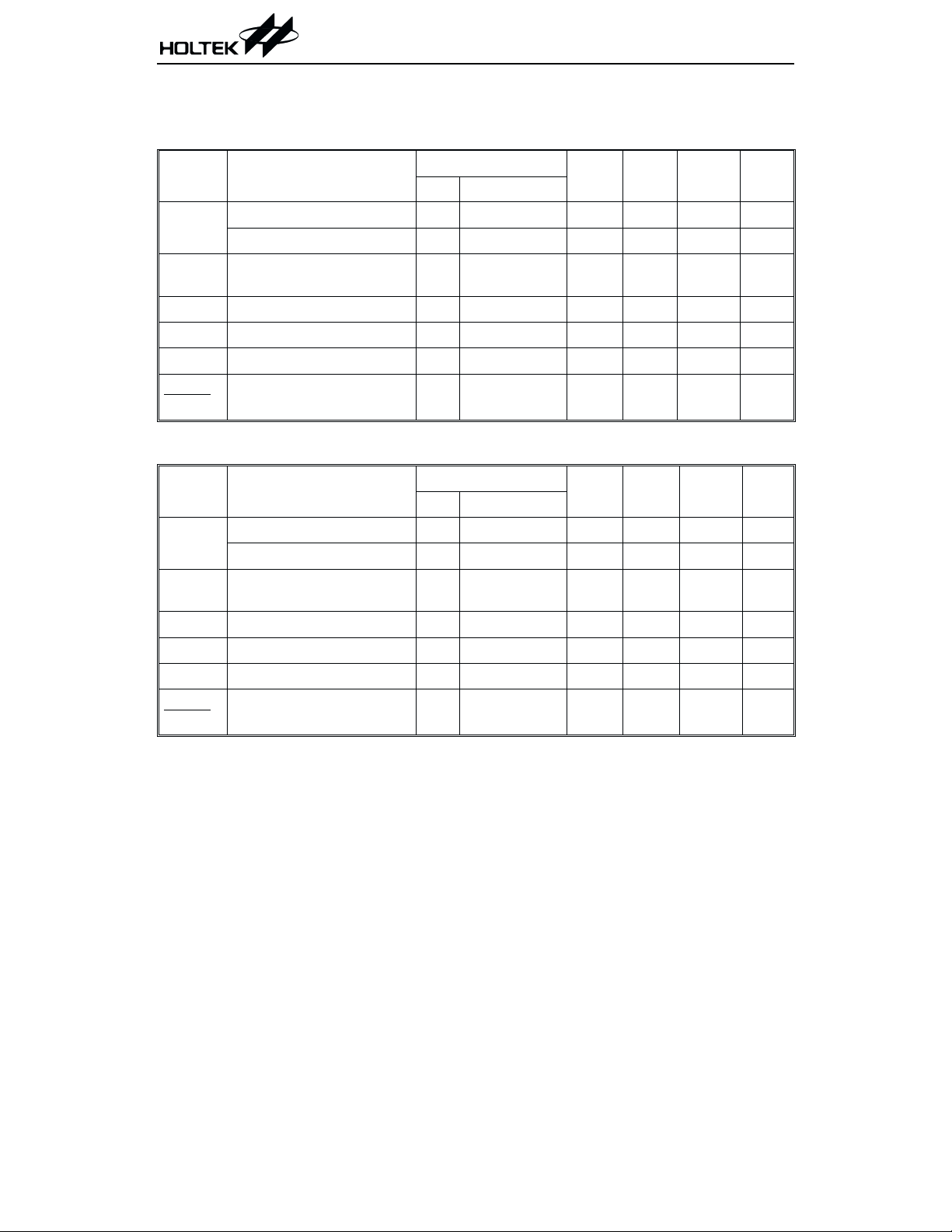
Electrical Characteristics
HT70XX
HT7024A
Symbol Parameter
V
V
I
V
I
DDV
DET
HYS
DD
DD
OL
DET
Hi®Lo Detectable Voltage ¾¾
Lo®Hi Detectable Voltage ¾¾
Hysteresis Width
Operating Current 8 No load
Operating Voltage
Output Sink Current 2
Temperature Coefficient
T
A
HT7027A
Symbol Parameter
V
V
I
V
I
DDV
DET
HYS
DD
DD
OL
DET
Hi®Lo Detectable Voltage ¾¾
Lo®Hi Detectable Voltage ¾¾
Hysteresis Width
Operating Current 8 No load
Operating Voltage
Output Sink Current 2
Temperature Coefficient
T
A
Ta=25°C
Test Conditions
Min. Typ. Max. Unit
V
DD
Conditions
2.28 2.4 2.52 V
2.325 2.52 2.772 V
¾¾
¾¾
V
=0.2V
OUT
0.02
V
DET
¾
1.5
0.5 1
0.05
V
DET
47
¾
0.1
V
DET
24 V
¾
mA
mA
¾ 0°C<Ta<70°C ¾±0.9 ¾ mV/°C
Ta=25°C
Test Conditions
Min. Typ. Max. Unit
V
DD
Conditions
2.565 2.7 2.835 V
2.616 2.835 3.118 V
¾¾
¾¾
V
=0.2V
OUT
0.02
V
DET
¾
1.5
0.5 1
0.05
V
DET
47
¾
0.1
V
DET
24 V
¾
mA
mA
¾ 0°C<Ta<70°C ¾±0.9 ¾ mV/°C
V
V
4 May 3, 2000

HT70XX
HT7033A
Symbol Parameter
V
V
I
V
I
DDV
DET
HYS
DD
DD
OL
DET
Hi®Lo Detectable Voltage ¾¾
Lo®Hi Detectable Voltage ¾¾
Hysteresis Width
Operating Current 8 No load
Operating Voltage
Output Sink Current 2.5
Temperature Coefficient
T
A
HT7039A
Symbol Parameter
V
V
I
V
I
DDV
DET
HYS
DD
DD
OL
DET
Hi®Lo Detectable Voltage ¾¾
Lo®Hi Detectable Voltage ¾¾
Hysteresis Width
Operating Current 8 No load
Operating Voltage
Output Sink Current 2.5
Temperature Coefficient
T
A
Ta=25°C
Test Conditions
V
DD
Conditions
Min. Typ. Max. Unit
3.135 3.3 3.465 V
3.197 3.465 3.811 V
¾¾
¾¾
V
=0.25V
OUT
0.02
V
DET
V
¾
1.5
1.2 2.5
0.05
DET
47
¾
0.1
V
DET
24 V
¾
mA
mA
¾ 0°C<Ta<70°C ¾±0.9 ¾ mV/°C
Ta=25°C
Test Conditions
Min. Typ. Max. Unit
DD
Conditions
V
3.705 3.9 4.095 V
3.779 4.095 4.504 V
¾¾
¾¾
V
=0.25V
OUT
0.02
V
DET
V
¾
1.5
1.2 2.5
0.05
DET
47
¾
0.1
V
DET
24 V
¾
mA
mA
¾ 0°C<Ta<70°C ¾±0.9 ¾ mV/°C
V
V
5 May 3, 2000

HT70XX
HT7044A
Symbol Parameter
V
V
I
V
I
DDV
DET
HYS
DD
DD
OL
DET
Hi®Lo Detectable Voltage ¾¾
Lo®Hi Detectable Voltage ¾¾
Hysteresis Width
Operating Current 8 No load
Operating Voltage
Output Sink Current 3.6
Temperature Coefficient
T
A
HT7050A
Symbol Parameter
V
V
I
V
I
DDV
DET
HYS
DD
DD
OL
DET
Hi®Lo Detectable Voltage ¾¾
Lo®Hi Detectable Voltage ¾¾
Hysteresis Width
Operating Current 8 No load
Operating Voltage
Output Sink Current 3.6
Temperature Coefficient
T
A
Ta=25°C
Test Conditions
Min. Typ. Max. Unit
V
DD
Conditions
4.18 4.4 4.62 V
4.263 4.62 5.082 V
¾¾
¾¾
V
=0.36V
OUT
0.02
V
¾
1.5
DET
0.05
V
DET
47
¾
36
0.1
V
DET
24 V
¾
V
mA
mA
¾ 0°C<Ta<70°C ¾±0.9 ¾ mV/°C
Ta=25°C
Test Conditions
Min. Typ. Max. Unit
V
DD
Conditions
4.75 5 5.25 V
4.845 5.25 5.775 V
¾¾
¾¾
V
=0.36V
OUT
0.02
V
DET
¾
2.1
0.05
V
DET
47
¾
36
0.1
V
DET
24 V
¾
mA
mA
¾ 0°C<Ta<70°C ¾±0.9 ¾ mV/°C
V
6 May 3, 2000

HT70XX
HT7070A
Symbol Parameter
V
V
I
V
I
DDV
DET
HYS
DD
DD
OL
DET
Hi®Lo Detectable Voltage ¾¾
Lo®Hi Detectable Voltage ¾¾
Hysteresis Width
Operating Current 8 No load
Operating Voltage
Output Sink Current 5
Temperature Coefficient
T
A
Test Conditions
V
DD
¾¾
¾¾
¾ 0°C<Ta<70°C ¾±0.9 ¾ mV/°C
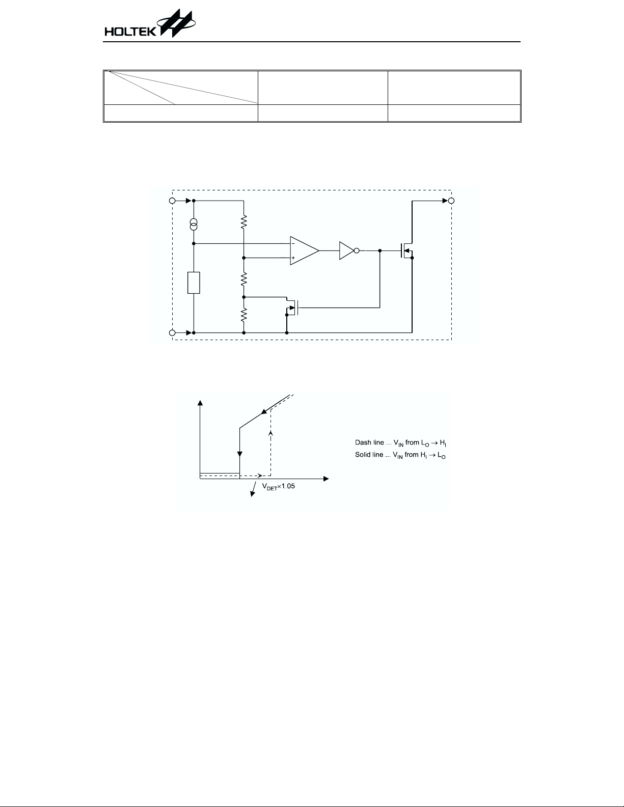
Functional Description
The HT70XX series is a set of voltage detectors
equipped with a high stability voltage reference
which is connected to the negative input of a
comparator¾ denoted as V
figure for NMOS output voltage detector.
When the voltage drop to the positive input of
the comparator (i,e,V
) is higher than V
B
VOUT goes high, M1 turns off, and V
pressed as V
=VDD´(RB+RC)/(RA+RB+RC).
BH
If VDD is decreased so that V
less than V
, the comparator output inverts
REF
from high to low, VOUT goes low, V
turns on, RC is bypassed, and V
=VDD´RB/(RA+RB), which is less than
V
BL
V
By so doing, the comparator output will
BH.
stay low to prevent the circuit from oscillating
when V
» V
B
REF.
If VDD falls below the minimum operating volt
age, the output becomes undefined. When VDD
goes from low to VDD´RB/(RA+RB) > V
comparator output and VOUT goes high.
The detectable voltage is defined as:
RA RB RC
V
(-)=
DET
++
RB RC
+
The release voltage is defined as:
RA RB
(+) =
V
DET
+
RB
´ V
REF
in the following
REF
falls to a value
B
´ V
REF
is ex-
B
is high, M1
C
becomes:
B
REF
REF
, the
Conditions
Min. Typ. Max. Unit
6.65 7 7.35 V
6.783 7.35 8.085 V
V
OUT
=0.5V
0.05
V
DET
47
¾
V
0.02
DET
¾
2.1
510
0.1
V
24 V
The hysteresis width is:
V
HYS=VDET
(+) - V
DET
(-)
The figure demonstrates the NMOS output
type with positive output polarity (VOUT is
normally open, active low). The HT70XX series
also supplies options for other output types
,
with active high outputs. Application circuits
shown are examples of positive output polarity
(normally open, active low) unless otherwise
specified.
RA
C om parator
V
B
V
C
-
V
REF
RB
M1
RC
NMOS output voltage detector (HT70XXA)
DET
¾
Ta=25°C
V
mA
mA
V
DD
V
OUT
MN
V
SS
RL
7 May 3, 2000

Application Circuits
HT70XX
Microcomputer reset circuit
Normally a reset circuit is required to protect
the microcomputer system from malfunctions
due to power line interruptions. The following
examples show how different output configura
tions perform a reset function in various sys
tems.
·
NMOS open drain output application for
separate power supply
V
DD1
V
OUT
Micro -
HT70XXA
·
NMOS open drain output application with
RESET
computer
V
DD2
V
SS
R-C delay
V
DD
R
HT70XXA
V
OUT
Micro computer
Power-on reset circuit
With several external components, the NMOS
open drain type of the HT70XX series can be
used to perform a power-on reset function as
shown:
-
-
V
IN
R
C
D
V
DD
V
OUT
HT7044A
V
SS
V
DD
V
OUT
V
OUT
V
SS
t
C
V
SS
t
8 May 3, 2000

HT70XX
5V power line monitoring circuit
Generally, a minimum operating voltage of
4.5V is guaranteed in a 5V power line system.
The HT7044A is recommended for use as 5V
power line monitoring circuit.
·
5V power line monitor with power-on reset
5V Power line
R
C
D
V
DD
V
OUT
HT7044A
V
SS
·
with 5V voltage regulator
5V Voltage regulator
V
IN
HT1050
GND
5V
V
DD
V
SS
V
OUT
HT7044A
V
SS
Change of detectable voltage
If the required voltage is not found in the stan
dard product selection table, it is possible to
change it by using external resistance dividers
or diodes.
·
Varying the detectable voltage with a resis
tance divider
V
IN
RA
RB
V
SS
Detectable voltage =
Hysteresis width =
·
Varying the detectable voltage with a diode
V
IN
RA RB
Vf1
Vf2
V
DD
V
DD
HT70XXA
RA RB
+
RB
+
RB
´ V
V
OUT
V
V
´ V
OUT
SS
DET
HYS
HT70XXA
V
SS
V
SS
-
-
Detectable Voltage = V
f1+Vf2+VDET
9 May 3, 2000

HT70XX
Malfunction analysis
The following circuit demonstrates the way a
circuit analyzes malfunctions by monitoring
the variation or spike noise of power supply
voltage.
V
DD
V
OUT
Charge monitoring circuit
The following circuit shows a charged monitor
for protection against battery deterioration by
overcharging. When the voltage of the battery
is higher than the set detectable voltage, the
transistor turns on to bypass the charge cur
rent, protecting the battery from overcharging.
HT70XXA
V
SS
V
SS
Level selector
The following diagram illustrates a logic level selector.
V
DD
V
OUT
HT7039A
V
V
SS
V
DD
DET2
Solar
Cell
V
OUT
HT7050A
V
DET1
-
V
DD
V
V
OUT
SS
Tr
BATT
HT70XXA
V
OUT
Load
5.0V
3.9V
V
DET1
V
DET2
V
OUT
t
t
10 May 3, 2000

HT70XX
Holtek Semiconductor Inc. (Headquarters)
No.3 Creation Rd. II, Science-based Industrial Park, Hsinchu, Taiwan, R.O.C.
Tel: 886-3-563-1999
Fax: 886-3-563-1189
Holtek Semiconductor Inc. (Taipei Office)
5F, No.576, Sec.7 Chung Hsiao E. Rd., Taipei, Taiwan, R.O.C.
Tel: 886-2-2782-9635
Fax: 886-2-2782-9636
Fax: 886-2-2782-7128 (International sales hotline)
Holtek Semiconductor (Hong Kong) Ltd.
RM.711, Tower 2, Cheung Sha Wan Plaza, 833 Cheung Sha Wan Rd., Kowloon, Hong Kong
Tel: 852-2-745-8288
Fax: 852-2-742-8657
Copyright Ó 2000 by HOLTEK SEMICONDUCTOR INC.
The information appearing in this Data Sheet is believed to be accurate at the time of publication. However, Holtek
assumes no responsibility arising from the use of the specifications described. The applications mentionedherein are
used solely for the purpose of illustration and Holtek makes no warranty or representation that such applications
will be suitable without further modification, nor recommends the use of its products for application that may pres
ent a risk to human life due to malfunction or otherwise. Holtek reserves the right to alter its products without prior
notification. For the most up-to-date information, please visit our web site at http://www.holtek.com.tw.
11 May 3, 2000
-
 Loading...