Features
Operating voltage: 2V~12V
·
Low power consumption
·
Built-in oscillator needs only 5% resistor
·
0/2/4/8 data selectable
·
224maximum address and data codes
·
Easy interface with an RF or IR medium
·
Applications
Burglar alarm system
·
Smoke and fire alarm system
·
Garage door controllers
·
Car door controllers
·
General Description
The HT6P20 is a CMOS LSI encoder designed
for remote control system applications. It en
codes 24 bits of information and then serially
transmits it via the DOUT pin upon receipt of
transmission enable (DATA pins: D0~D7) signals. The combination of address and data bits
of the HT6P20 is designed using one time pro-
HT6P20
24
2
One time programmable process
·
Data active: D0~D7
·
Minimal external components
·
HT6P20/A/B: 8-pin DIP/NSOP package
·
HT6P20/D: 16-pin DIP/NSOP package
Security system
·
Cordless telephones
·
Other remote control systems
·
grammable process. In addition, the chip offers
various packaging for flexible combination of
programmable address/data so as to meet vari
ous applications. Its programmable ad
dress/data is transmitted together with the
anti-code bits via RF or infrared transmission
medium upon receipt of a trigger signal.
OTP Encoder
-
-
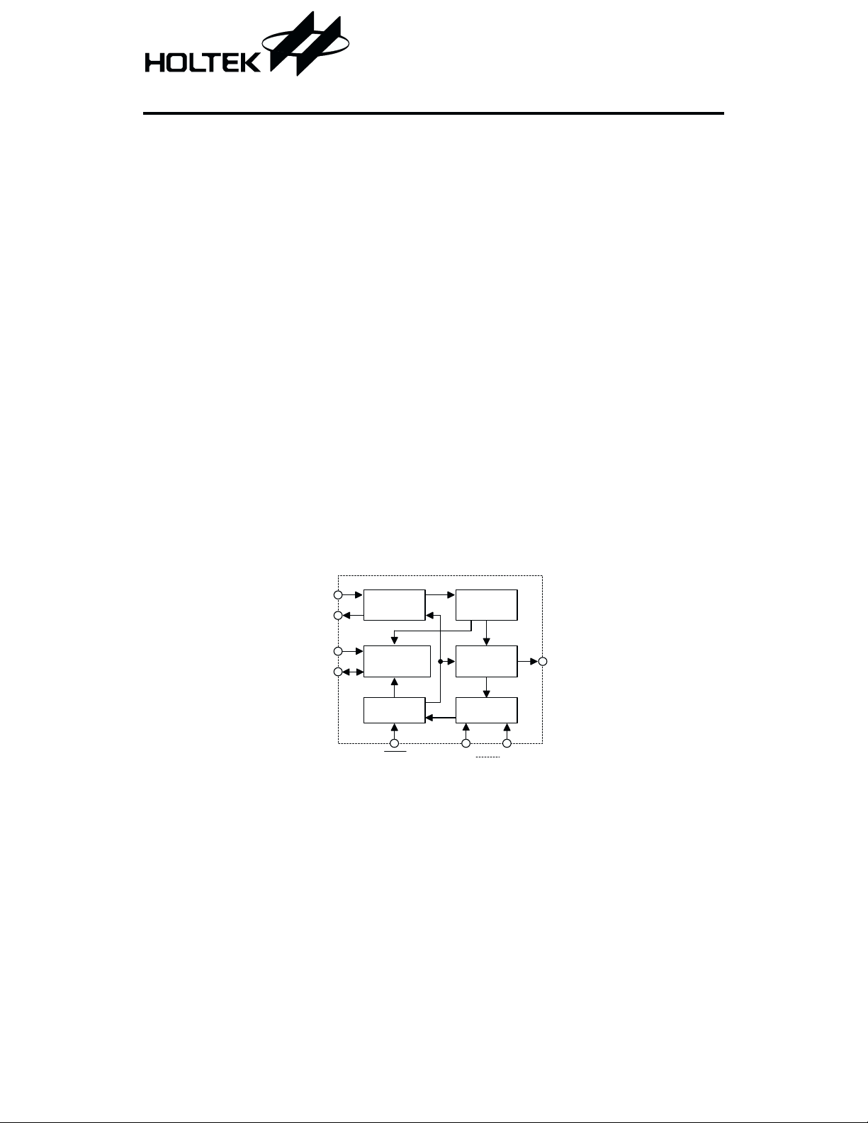
Block Diagram
OSC1
OSC2
VPP
SIO
Note: Address/Data numbers are available in various combinations, refer to the functional descrip
tion.
Oscillator
Program m ing
Circuit
C ontrol U nit
PGM
Address
C ounter
Mixer &
Driver
D a ta L a tc h
D0 D7
1 May 2, 2000
DOUT

Pin Assignment
HT6P20
24-A ddress
0 -D a ta
PGM
1
VSS
2
OSC2
3
OSC1
4
H T6P 20A
8 D IP /N S O P
SIO
8
VPP
7
VDD
6
DOUT
5
22-A ddress
2 -D a ta
D0
1
D1
2
VSS
3
OSC2
4
HT6P20B
8 D IP /N S O P
B lank device B lank device
D1
1
PGM
VSS
OSC2
OSC1
1
2
3
4
8
7
6
5
HT6P20
8 D IP /N S O P
SIO
VPP
VDD
DOUT
D2/NC
D3/NC
D4/NC
D5/NC
D6/NC
D7/NC
2
3
VSS
4
5
6
7
8
HT6P20
1 6 D IP /N S O P
20-A ddress
4 -D a ta
D1
D2
D3
VSS
NC
8
VDD
7
DOUT
6
OSC1
5
NC
NC
NC
NC
16
1
2
3
4
5
6
7
8
D0
15
PGM
14
SIO
13
VPP
12
VDD
11
DOUT
10
OSC1
9
OSC2
HT6P20D
1 6 D IP /N S O P
D0
16
PGM
15
SIO
14
VPP
13
VDD
12
DOUT
11
OSC1
10
OSC2
9
Note:
The customer code and control code have been programmed into HT6P20A/B/D by Holtek¢s
factory process.
The blank device HT6P20 is not programmed, it can be programmed by Holtek¢s programming
kit.
Warning: The 8-pin blank device only allows programming as HT6P20A type.
The 16-pin blank device allows programming as one of HT6P20/D type. After program
ming the HT6P20 pin name are the same as one of HT6P20D, which is determined by the
kit programming procedure.
Pin name ²NC² stands for no connection (floating).
2 May 2, 2000
-

HT6P20
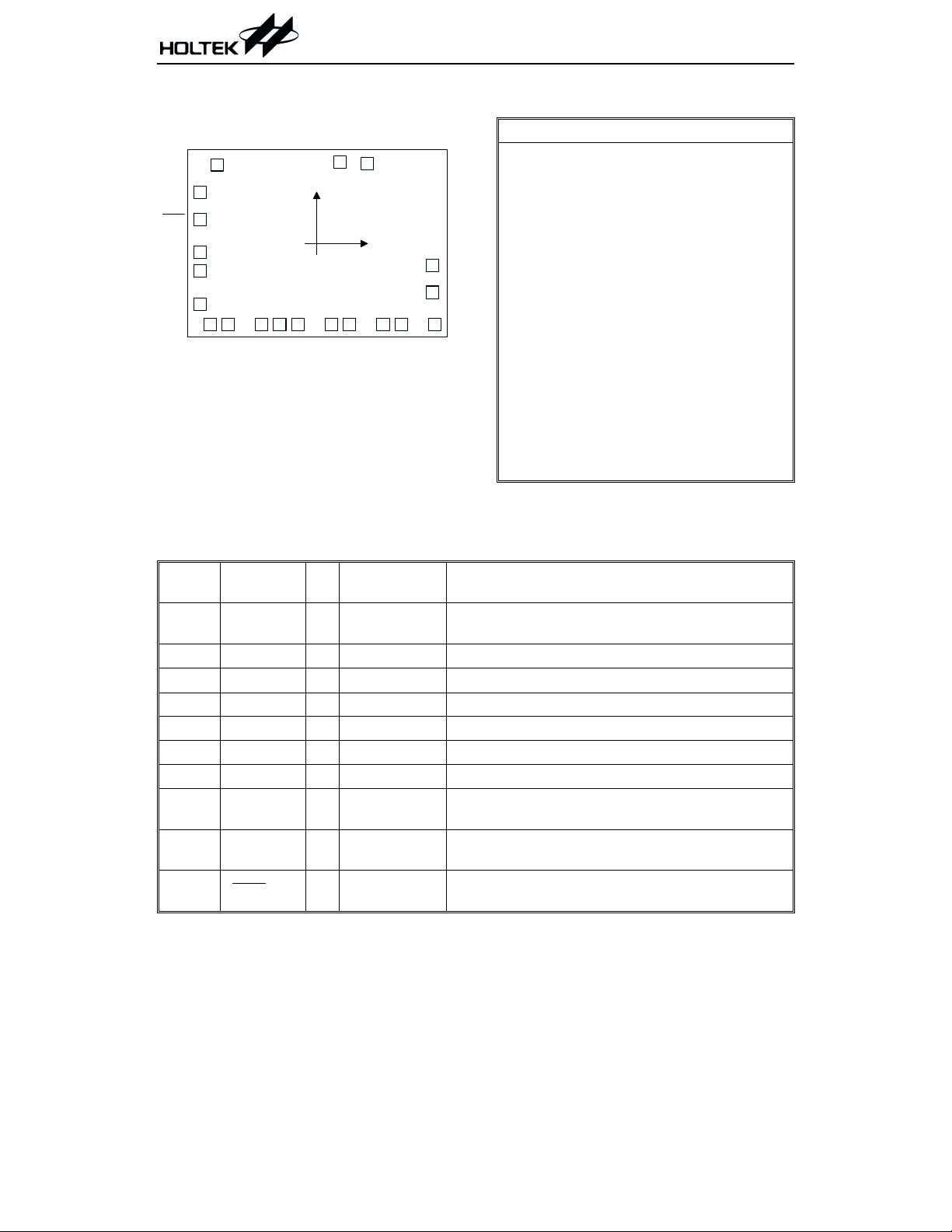
Pad Assignment Pad Coordinates
DOUT
NC
VDD
20
(0 ,0 )
12 13
D4
D5
19
14 15
D6
NC
18
17
16
OSC1
OSC2
D7
Pad No. X Y
1
2
3
4
5
6
7
-1123.00
-1123.00
-1123.00 -86.25
-1123.00 -261.25
-1123.00 -583.75
-1027.50 -776.75
8
9
10
11
12 142.50
SIO
PGM
D0
NC
D1
2
3
4
5
6
VPP
1
7 8
D2
D3
9 10 11
VSS
NC
13 317.50
14 640.00
Chip size: 2590 ´ 2010 (mm)
2
* The IC substrate should be connected to VSS in
the PCB layout artwork.
15 815.00
16 1137.50
17 1118.00
18 1118.00
19 489.00 772.05
20 223.50 789.75
Pin Description
HT6P20D
Pin No. Pin Name I/O
16
1~3
4 VSS
5~8 NC
D0~D3 I
¾¾
¾¾
9 OSC2 O OSCILLATOR Oscillator output pin
10 OSC1 I OSCILLATOR Oscillator input pin
11 DOUT O CMOS OUT Data serial transmission output
12 VDD
¾¾
13 VPP I
14 SIO I/O
15 PGM
Connection
I
Internal
CMOS IN
Pull-high
¾
CMOS
IN/OUT
CMOS IN
Pull-high
Description
Data input and transmission enable (active low)
They can be externally set to VSS or left open.
Negative power supply, ground
No connection
Positive power supply
Programming power supply, V
tion
Programming address/control code input and mode
code output for mode verification
Program mode control pin, active low
Unit: mm
-956.50
762.75
498.75
236.25
-852.50 -776.75
-530.00 -776.75
-355.00 -776.75
-180.00 -776.75
-776.75
-776.75
-776.75
-776.75
-776.75
-466.75
-205.75
for normal opera
DD
-
3 May 2, 2000
 Loading...