


3
18
Series of Decoders
Selection Table
Function
Address
No.
Data
VT Oscillator Trig ger Package
Item No. Type
HT602L 12 2 L
√
RC oscillator DIN active “Hi” 20 DIP/20 SOP
HT604L 10 4 L
√
RC oscillator DIN active “Hi” 20 DIP/20 SOP
HT605L 9 5 L
√
RC oscillator DIN active “Hi” 20 DIP/20 SOP
HT611 14 0 —
√
RC oscillator DIN active “Hi” 20 DIP/20 SOP
Features
•
Operating voltage: 2.4V~12V
•
Low power and high noise immunity CMOS
technology
•
Low standby current
•
Capable of decoding 18 bits of information
•
Pairs with HOLTEK’s 318 series of encoders
•
8~18 address pins
•
0~8 data pins
•
Trinary address setting
•
Two times of receiving check
•
Built-in oscillato r needs only a 5% resistor
•
Valid transmission indictor
•
Easily interface with an RF or an infrared
transmission medium
•
Minimal external components
General Description
The 318 decoders are a series of CMOS LSIs for
remote control system applications. They are
paired with the 3
18
series of encoders. For
proper operation a pair of encoder/decoder pair
with the same number of address and data
format should be selected (refer to the encoder/decoder cross reference tables).
The 3
18
series of decoders receives serial address and data from that series of encoders that
are transmitted by a carrie r using an R F or a n
IR transmission medium. It then compares the
serial input data twice continuously with its
local address. If no errors or unma tched codes
are encountered, the input data codes are decoded and then transferred to the outp ut pins.
The VT pin also goes high to indicate a valid
transmission.
The 3
18
decoders are capable of decoding 18 bits
of information that consists of N bits of address
and 18–N bits of data. To meet various applications they are arranged to provi de a nu mber of
data pins whose range is from 0 to 8 and an
address pin whose range is from 8 to 18. In
addition, the 3
18
decoders provide various combinations of address/d ata number in different
packages.
Applications
•
Burglar alarm system
•
Smoke and fire alarm system
•
Garage door controllers
•
Car door controllers
•
Car alarm system
•
Security system
•
Cordless telephones
•
Other remote control systems
1 2nd Oct ’97
Function
Address
No.
Data
VT Oscillator Trigger Package
Item No. Type
HT612 12 2 M
√
RC oscillator DIN active “Hi” 20 DIP/20 SOP
HT614 10 4 M
√
RC oscillator DIN active “Hi” 20 DIP/20 SOP
HT615 9 5 M
√
RC oscillator DIN active “Hi” 20 DIP/20 SOP
HT644L 14 4 L
√
RC oscillator DIN active “Hi” 24 SOP/24 SDIP
HT646L 12 6 L
√
RC oscillator DIN active “Hi” 24 SOP/24 SDIP
HT648L 10 8 L
√
RC oscillator DIN active “Hi” 24 SOP/24 SDIP
HT651 18 0 —
√
RC oscillator DIN active “Hi” 24 SOP/24 SDIP
HT654 14 4 M
√
RC oscillator DIN active “Hi” 24 SOP/24 SDIP
HT656 12 6 M
√
RC oscillator DIN active “Hi” 24 SOP/24 SDIP
HT658 10 8 M
√
RC oscillator DIN active “Hi” 24 SOP/24 SDIP
HT682L 10 2 L
√
RC oscillator DIN active “Hi” 18 DIP
HT683L 9 3 L
√
RC oscillator DIN active “Hi” 18 DIP
HT684L 8 4 L
√
RC oscillator DIN active “Hi” 18 DIP
HT691 12 0 —
√
RC oscillator DIN active “Hi” 18 DIP
HT692 10 2 M
√
RC oscillator DIN active “Hi” 18 DIP
HT693 9 3 M
√
RC oscillator DIN active “Hi” 18 DIP
HT694 8 4 M
√
RC oscillator DIN active “Hi” 18 DIP
Note: Data type: M represents momentary type of data output.
L represents latch type of data output.
VT can be used as a momentary data output.
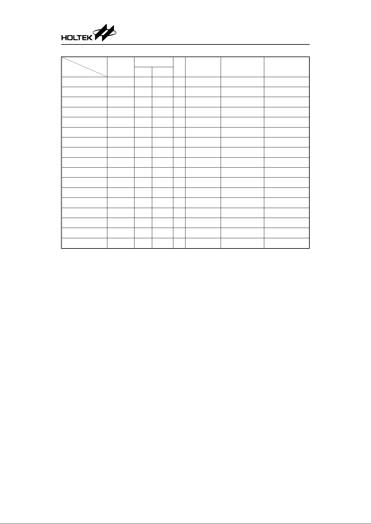
318 Series of Decoders
2 2nd Oct ’97
Block Diagram
Note: The address/data pins are available in various combinations
(refer to the address/data table).
Pin Description
Pin Name I/O
Internal
Connection
Description
A0~A17 I
TRANSMISSION
GATE
Input pins for address A0~A17 setting
They can be externally set to VDD , VS S, or left open.
D10~D17 O CMOS OUT Output data pins
DIN I CMOS IN Serial data input pin
VT O CMOS OUT Valid transmission, active high
OSC1 I OSCILLATOR Oscillator input pin
OSC2 O OSCILLATOR Oscillator output pin
VSS I — Negative power supply (GND)
VDD I — Positive power supply
318 Series of Decoders
3 2nd Oct ’97
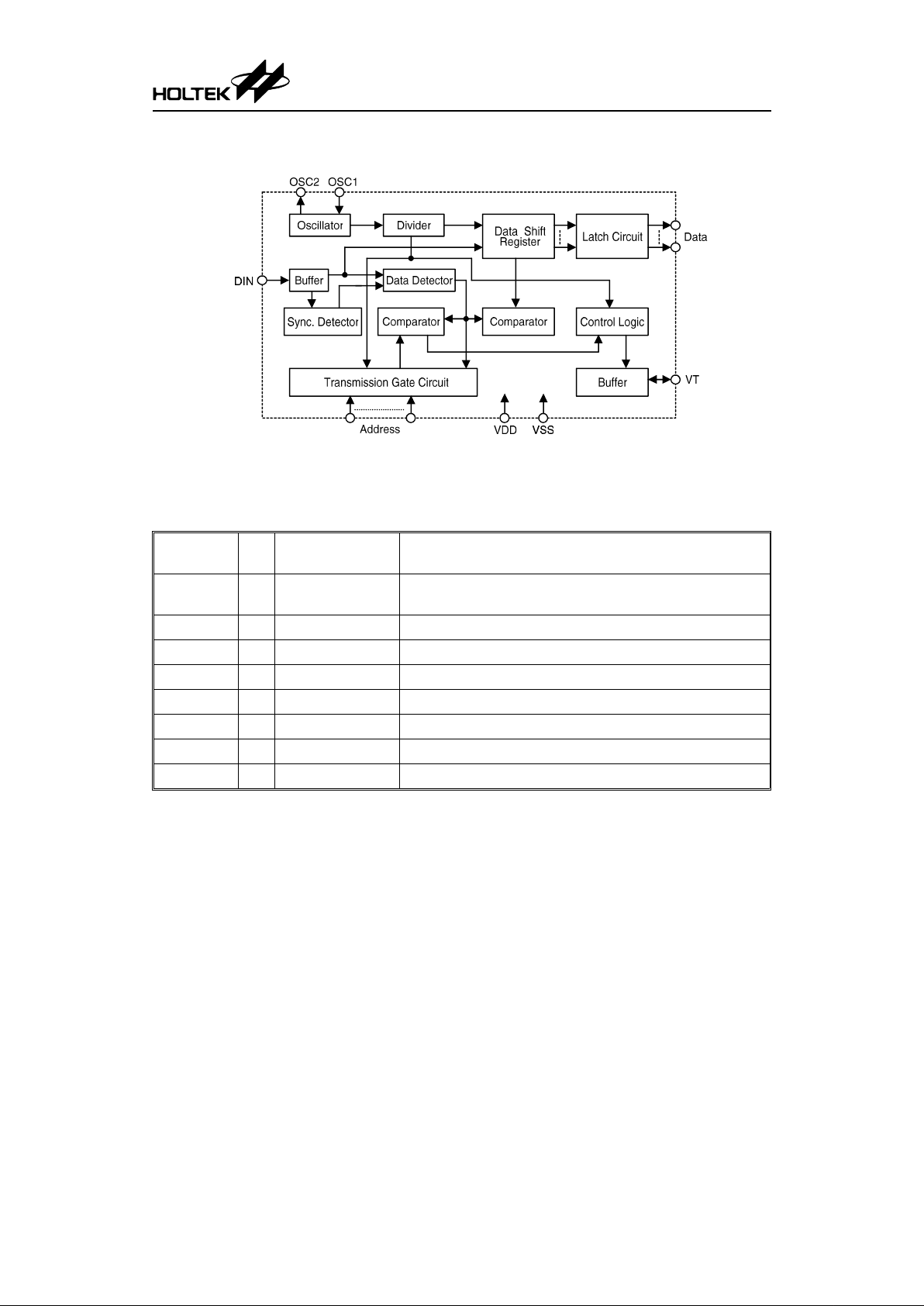
Approximate i nte r na l connection circu i t s
Absolute Maximum Ratings*
Supply Voltage...............................–0.3V to 13V
Storage Temperature.................–50
°C to 125°C
Input Voltage..................V
SS
–0.3V to VDD+0.3V
Operating Temperature...............–20
°C to 75°C
*Note: Stresses above those listed under “Absolute Maximum Ratings” may cause permanent
damage to the device. The se are stress ratings on ly. Functional operatio n of this device at
these or any other conditions above those indicated in the operational sections of this
specification is not implied and exposure to absolute maximum rating conditions for extened
periods may affect device relia bility.
Electrical Characteristics
(Ta=25°C)
Symbol Parameter
Test Conditions
Min. Typ. Max. Unit
V
DD
Conditions
V
DD
Operating Voltage — — 3 — 12 V
I
STB
Standby Current
5V
Oscillator stops
— 0.1 1
µA
12V — 2 4
µA
I
DD
Operating Current 5V
No load
F
OSC
=100kHz
— 0.2 1 mA
I
O
Data Output Source Current
(D10~D17)
5V
V
OH
=4.5V –0.5 –1 — mA
Data Output Sink Current
(D10~D17)
V
OL
=0.5V 0.5 1 — mA
I
VT
VT Output Source Curren t
5V
VOH=4.5V –2 –4 — mA
VT Output Sink Current V
OL
=0.5V 1 2 — mA
V
IH
“H” Input Voltage 5V — 3.5 — 5 V
V
IL
“L” Input Voltage 5V — 0 — 1 V
F
OSC
Oscillator Freque ncy 10V
R
OSC
=330kΩ
—100—kHz
318 Series of Decoders
4 2nd Oct ’97
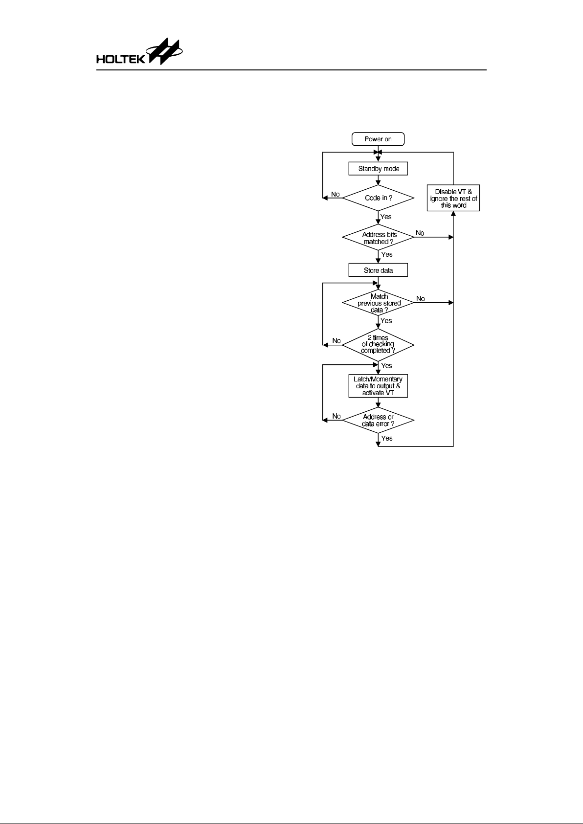
Functional Description
Operation
The 318 series of decoders provides various combinations of address and data pins i n different
packages. It is paired with the 3
18
series of
encoders. The d ecoders receive data transmitted by the encoders a nd interpret the first N
bits of the code period as address and the last
18–N bits as data (where N is the address code
number). A signal on the DIN pin then activates
the oscillator which in turns decodes the incoming address and data. The decoders will check
the received address twice continuously. If all
the received ad dress code s match the conten ts
of the decoder ’s local add ress, the 18–N bits of
data are decoded to activate the output pins,
and the VT pin is set high to indica te a valid
transmission. Th at will last until the ad dress
code is incorrect or no signal has been received.
The output of the VT pin is high only when the
transmission is valid. Otherwise it is low always.
Output type
There are 2 types of output to select from:
•
Momentary type
The data outputs follow the encoder during a
valid transmission and then reset.
•
Latch type
The data outputs follow the encoder during a
valid transmission, and are then latched in
this state until the next valid transmission
occurs.
Flowchart
Note: The oscillator is disabled in the
standby state and activated as long as
a logic “high” signal is applied to the
DIN pin. i.e., the DIN should be kept
“low” if there is no signal input.
318 Series of Decoders
5 2nd Oct ’97