

Features
•
Support the ANSI X3.131-1986 standard
•
Asynchronous transfer rate to 5 Mbyte/sec
•
Support initiator and target mode
•
0.8um CMOS process
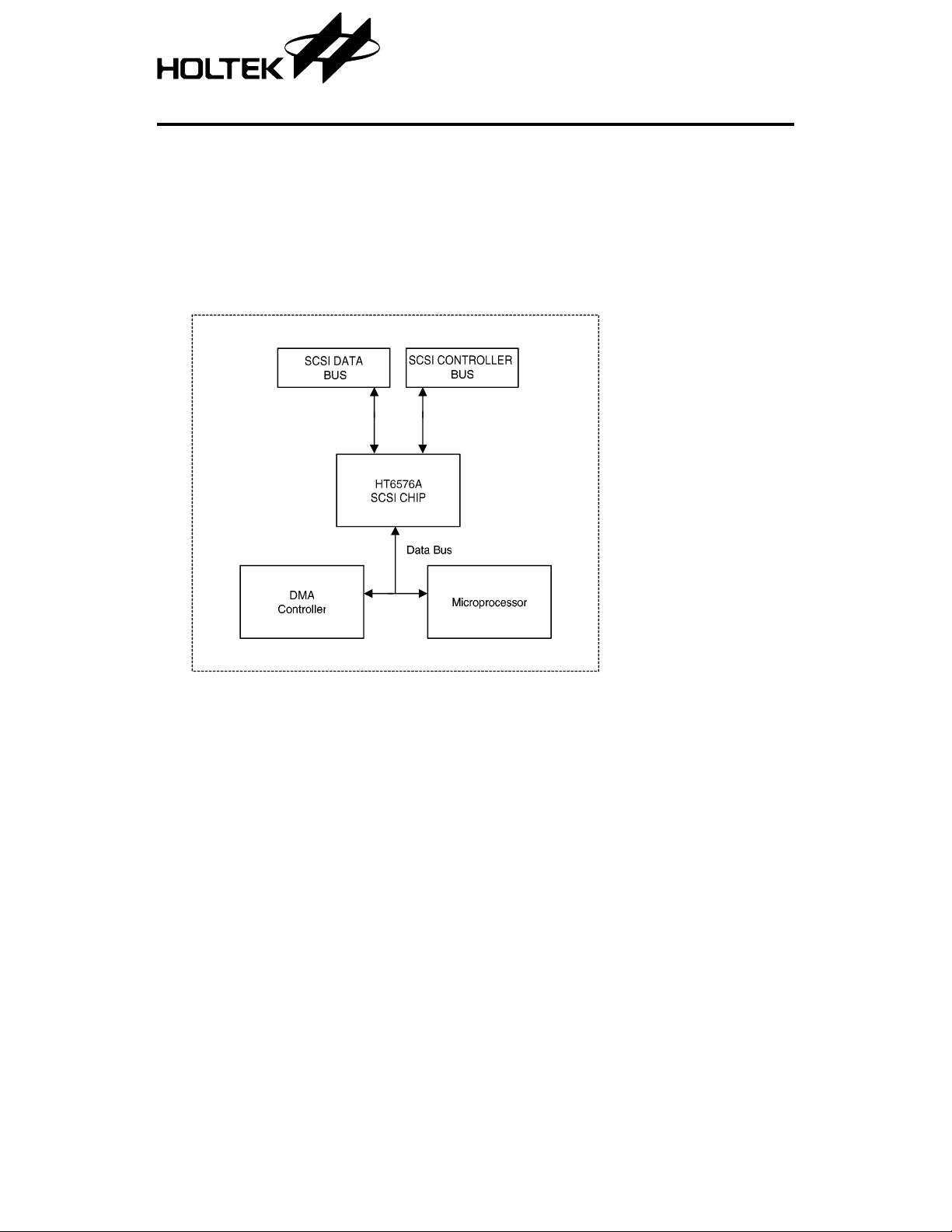
Block Diagram
HT6576A
Advanced SCSI CHIP
•
On chip 48mA single-ended drivers and
receivers
•
Non internal clock needed
•
44pins PLCC package
1 14th July ’97
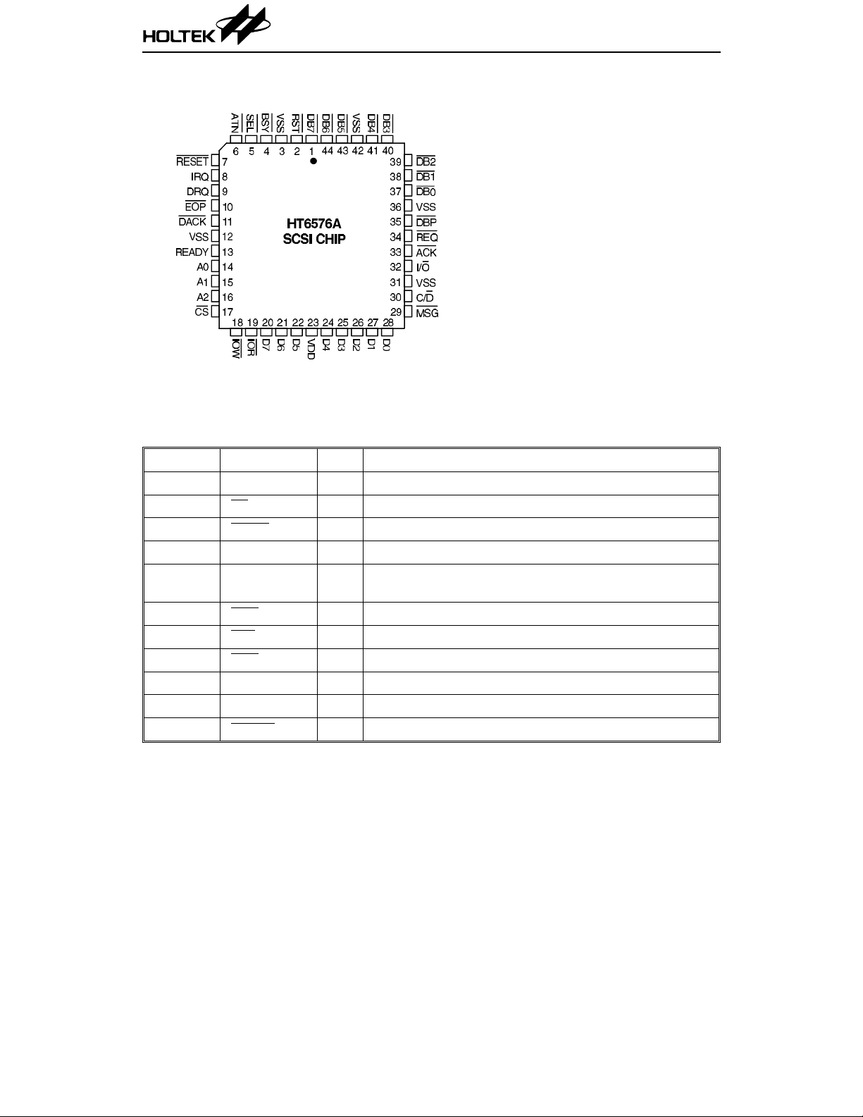
Pin Diagram
Pin Description
Host Interface Signal
Pin No Pin Name I/O Description
14~16 A0~A2 I Address Lines
17
11
9 DRQ O DMA Request
24~28,
20~22
10
19
18
8 IRQ O Interrupt Request
13 READY O Ready
7
CS I Chip Select, active low
DACK I DMA Acknowledge, active low
D0~D7 I/O Data Lines
EOP I End of Process, active lo w
IOR I I/O Read, active low
IOW I I/O Write, active low
RESET I Reset, active low
HT6576A
2 14th July ’97
SCSI Interface Signals
Pin No Pin Name I/O Description
33 ACK I/O Acknowledge, active low
6
4
30 C/
32 I/
29
34
2
37~41,
43, 44, 1
35
5
VSS
3, 12, 31, 36, 42
ATN I/O Attention, active low
BSY I/O Busy, active low
D I/O Control/Data, active low
O I/O Input/Output, active low
MSG I/O Message, active low
REQ I/O Request, active low
RST I/O Reset, active low
DB0–DB7 I/O SCSI Data Bus, active low
DBP I/O SCSI Parity Bit, active low
SEL I/O Select, active low
HT6576A
VDD
23
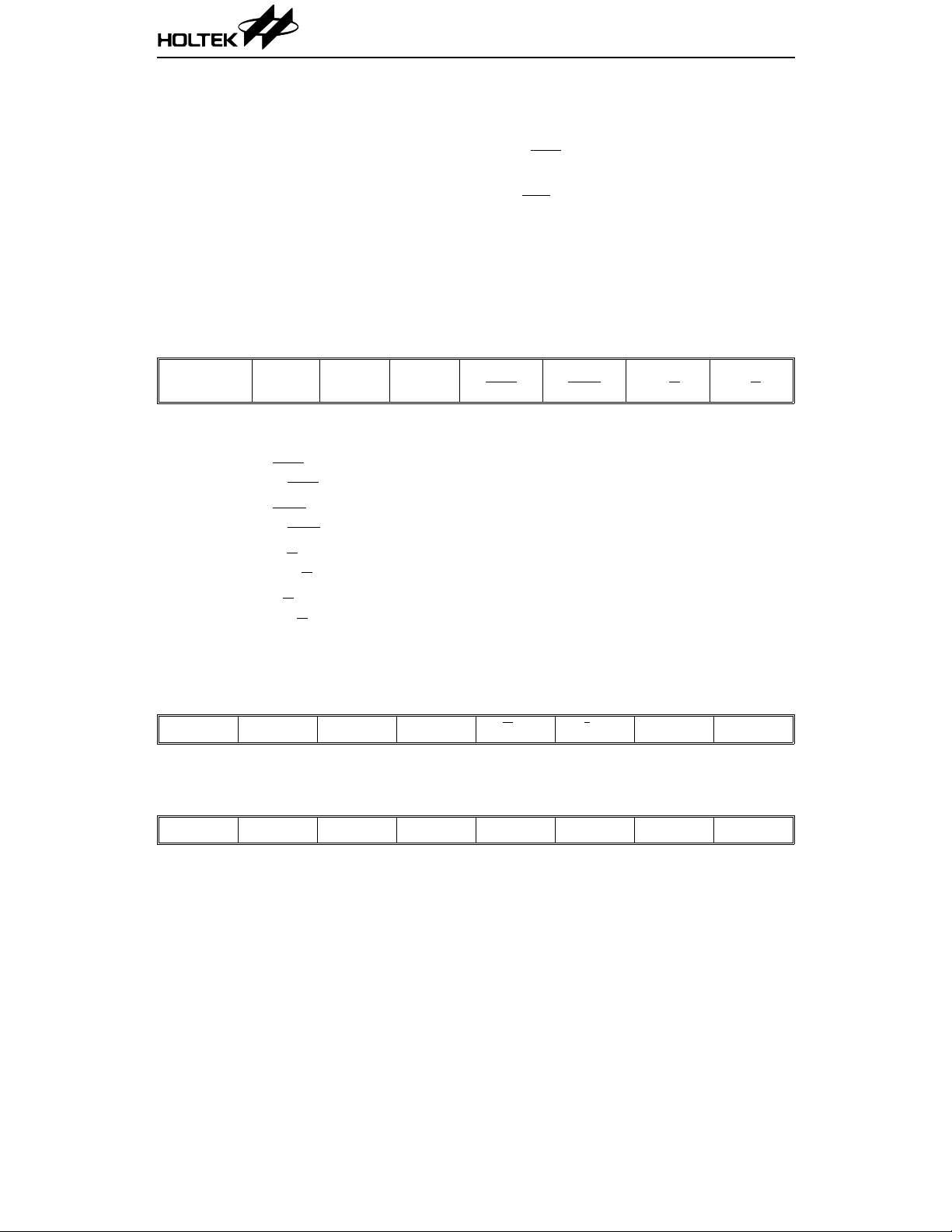
Registers
Address 0
Current SCSI data register(READ ONL Y)
DB7 DB6 DB5 DB4 DB3 DB2 DB1 DB0
The SCSI bus parity is checked at the beginning of the read cycle.
Output data register(WRITE ONLY)
DB7 DB6 DB5 DB4 DB3 DB2 DB1 DB0
3 14th July ’97
HT6576A
Address 1: Init iator command registe r
WRITE
7 6 5 4 3 2 1 0
ASSERT
RST
•
BIT 7: ASSERT RST
WHEN SET, THE
•
BIT 6: TRI–STATE (TEST MODE)
•
BIT 5: RESERVED (0)
•
BIT 4: ASSERT ACK
WHEN SET, THE
•
BIT 3: ASSERT BSY
WHEN SET, THE
•
BIT 2: ASSERT SEL
WHEN SET, THE
•
BIT 1: ASSERT ATN
WHEN SET, THE
•
BIT 0: ASSERT DATA
TRI–STATE RESERVED
RST SIGNAL IS ASSERTED ON THE SCSI BUS
ACK SIGNAL IS ASSERTED ON THE SCSI BUS
BSY SIGNAL IS ASSERTED ON THE SCSI BUS
SEL SIGNAL IS ASSERTED ON THE SCSI BUS
ATN SIGNAL IS ASSERTED ON THE SCSI BUS
WHEN SET, This bit allows the contents of the output data register to be enabled as chip outputs
on SCSI signal
DB0–DB7
ASSERT
ACK
ASSERT
BSY
ASSERT
SEL
ASSERT
ATN
ASSERT
DATA
READ
7 6 5 4 3 2 1 0
RET
ARBIT
PROGRESS
LOST
ARBIT
ACK BSY SEL ATN
ASSERT
DATA
Address 2: Mode register
READ/WRITE
7 6 5 4 3 2 1 0
LOCK
DMA
•
BIT 7: BLOCK MODE DMA
•
BIT 6: TARGET MODE
TARGET
MODE
ENABLE
PARITY
ENABLE
PARITY
ENABLE
EOP
MONITOR
CHECK
BUSY
DMA
IRQ
MODE
ARBIT
When set, the chip ope rates as an SCSI bus target device.
•
BIT 5: ENABLE PARITY CHECKING
When set, data received on the SCSI data bus is checked for odd parity.
4 14th July ’97
HT6576A
•
BIT 4: ENABLE PARITY INTERRUPT
When set, this bit causes the IRQ signal to be asserted if a parity error is detected.
•
BIT 3: ENABLE EOP INTERRUPT
When set, this bit causes the IRQ signal to be asserted if
•
BIT 2: MONITOR BUSY
When set, this bit causes the IRQ signa asserted when
least a bus settle delay.
•
BIT 1: DMA MODE
•
BIT 0: Arbitrate
When set, this bit starts the arbitration process.
Address 3: Target command register
7 6 5 4 3 2 1 0
LAST BYTE X X X
ASSERT
R R/W R/W R/W R/W
•
BIT 7: LAST BYTE SEND (READ ONLY)
•
BIT 3: ASSERT REQ
WHEN SET, THE
•
BIT 2: ASSERT MSG
WHEN SET, THE
•
BIT 1: ASSERT C/D
WHEN SET, THE C/
•
BIT 0: ASSERT I/O
WHEN SET, THE I/
REQ SIGNAL IS ASSERTED ON THE SCSI BUS (IN TARGET MODE)
MSG SIGNAL IS ASSERTED ON THE SCSI BUS (IN TARGET MODE)
D SIGNAL IS ASSERTED ON THE SCSI BUS (IN TARGET MODE)
O SIGNAL IS ASSERTED ON THE SCSI BUS (IN TAGRTE MODE)
EOP is received from the DMA controller .
BSY changes to the inactive state for at
REQ
ASSERT
MSG
ASSERT
C/D
ASSERT
I/O
Address 4: Current SCSI Bus Register
READ
7 6 5 4 3 2 1 0
RST BSY REQ MSG C/D I/O SEL DBP
WRITE –SELECT ENABLE REGISTER
7 6 5 4 3 2 1 0
SID7 SID6 SID5 SID4 SID3 SID2 SID1 SID0
5 14th July ’97

HT6576A
Address 5: Bus And Status
READ
7 6 5 4 3 2 1 0
END
DMA
WRITE –START DMA SEND
7 6 5 4 3 2 1 0
XXXXXXXX
Address 6: Input Data
READ
7 6 5 4 3 2 1 0
LDB7 LDB6 LDB5 LDB4 LDB3 LDB2 LDB1 LDB0
LATCH SCSI DAT A. The register represent the complement of the active low SCSI data bus.
WRITE –START DMA TARGET RECEIVE
7 6 5 4 3 2 1 0
XXXXXXXX
DMA
REQUEST
PARITY
ERROR
IRQ
PHASE
MATCH
BUS ERROR ATN ACK
Address 7:
READ –RESET PARITY/INTERRUPT
7 6 5 4 3 2 1 0
XXXXXXXX
WRITE –START DMA INITIATOR RECEIVE
7 6 5 4 3 2 1 0
XXXXXXXX
6 14th July ’97

HT6576A
Interrupts
SELECTION/RESELECTION
•
SEL= ACTIVE LOW
•
BSY IS FALSE FOR AT LEAST 400NS
•
HT6576A DEVICE ID (SELECT REGISTER) is active on the SCSI bus will generate IRQ.
END OF PROCESS (EOP) INTERRUPT
•
EOP= ACTIVE LOW
•
DACK= ACTIVE LOW
•
IOR OR IOW= ACTIVE LOW
•
DMA MODE
•
ENABLE EOP IRQ⇒ GENERATE EOP IRQ
SCSI BUS RST/IRQ
When An SCSI RST active low, the IRQ is generated.
PARITY ERROR IRQ
An IRQ is generated for a received parity error if enable parity checking bit and the enable
parity interrupt bit are set.
BUS PHASE MISMATCH IRQ
If the DMA MODE bit is active and a phase mismatch occurs when REQ from false to true,
an interrupt is generated
LOSS OF BSY/IRQ
•
MONITOR BSY bit= 1
•
BSY= ACTIVE LOW FOR 400ns WILL GENERATE IRQ
7 14th July ’97

HT6576A
Electrical Characteristics
D.C. Characteristics
Absolute Maximum Ratings (Ta=25°C)
Symbol Parameter Min. Max. Unit
Tstg Storage Temperature –55 150 °C
V
DD
V
IN
ESD Electrostatic Discharge –5000 5000 V
Supply Voltage –0.5 7.0 V
Input Voltage VSS–0.5 VDD+0.5 V
Operating Conditions (Ta=25
Symbol Parameter Min. Max. Unit
V
DD
I
DD
Ta Operating Free-Air 0 70
Supply Voltage 4.75 5.25 V
Supply Current — 20 mA
°C
SCSI Signals (Ta=25
Symbol Characteristic Condition Min. Max. Unit
V
V
V
V
I
I
I
IH
IL
OL
HYS
OL
IH
IL
Input High Voltage — 2.0 VDD+0.5 V
Input Low Voltage — VSS–0.5 0.8 V
Output Low Voltage IOL=48mA V
SS
0.5 V
Hysteresis — 200 450 mV
Output Low Current VOL=0.5 48 — mA
Input High Leakage VIH= 5.25V — 50 µA
Input Low Leakage VIL=V
SS
—–50µA
°C)
°C)
8 14th July ’97

HT6576A
Microprocessor Data Bus D0-D7 (Ta=25°C)
Symbol Characteristic Condition Min. Max. Unit
V
IH
V
IL
V
OH
V
OL
I
OH
I
OL
I
IH
I
IL
I
TL
Input High Voltage — 2.0 VDD+0.5 V
Input Low Voltage — VSS–0.5 0.8 V
Output High Voltage IOH=–4.0mA 2.4 V
Output Low Voltage IOL=8.0mA V
SS
DD
0.4 V
V
Output High Current VOH=VDD–0.5V –4.0 — mA
Output Low Current VOL=0.4V 8.0 — mA
Input High Leakage VIH=5.25V — 10 µA
Input Low Leakage VIL=V
SS
—–10µA
Tri-State Leakage — –10 10 µA
A0~A2,
CS, EOP, IOR, IOW, RESET (Ta=25°C)
Symbol Characteristic Condition Min. Max. Unit
V
IH
V
IL
I
IH
I
IL
Input High Voltage — 2.0 VDD+0.5 V
Input Low Voltage — VSS–0.5 0.8 V
Input High Leakage VIH=5.25V 10 — µA
Input Low Leakage VIL=V
SS
–10 — µA
DRQ, IRQ, READY,
Symbol Characteristic Condition Min. Max. Unit
V
OH
V
OL
I
OH
I
OL
Output High Voltage IOH=–4.0mA 2.4 V
Output Low Voltage IOL=8.0mA V
SS
DD
0.4 V
Output High Current VOH=VDD–0.5V –4.0 — mA
Output Low Current VOL=0.4V 8.0 — mA
V
9 14th July ’97

Timing Diagram
Initiator Send
HT6576A
Name Description Min. Max. Unit
t1 SCSI Data setup time to ACK active 40 — ns
t2 Data Bus held time from
t3
t4
t5
t6
IOW active time 30 — ns
DACK active, to DRQ inactive — 20 ns
ACK active to next DRQ active — 45 ns
EOP active time 30 — ns
IOW inactive 10 — ns
10 14th July ’97

Initiator Receive
HT6576A
Name Description Min. M ax. Unit
t1 IOR inactive to next REQ active 50 — ns
t2
t3
t4
t5 Data Bus hold time from
t6 Data Bus valid time from
t7
t8
t9
t10
REQ active to ACK active 50 — ns
IOR inactive to ACK inactive 10 — ns
ACK inactive time 50 — ns
IOR inactive 10 — ns
IOR active — 20 ns
REQ active to DRQ active — 25 ns
DACK active to DRQ inactive — 20 ns
DACK inactive to next DRQ active 20 — ns
EOP active time 30 — ns
11 14th July ’97

Target Send (Non-block mode)
HT6576A
Name Description Min. Max. Unit
t1 SCSI data hold time from IOW inactive — 30 ns
t2 SCSI data setup time to
t3
t4 Data Bus setup time to
t5 Data Bus hold time from
t6
t7
t8
t9
ACK active to REQ inactive — 30 ns
IOW active time 30 — ns
DACK active to DRQ inactive — 20 ns
IOW inactive to DACK inactive 0 — ns
ACK active to next DRQ active — 45 ns
REQ active 40 — ns
IOW inactive 10 — ns
IOW inactive 10 — ns
12 14th July ’97

Target Receive (Non-block mo de )
HT6576A
Name Description Min. M ax. Unit
t1 ACK inactive to next REQ active 50 — ns
t2
t3
t4 Data Bus setup time to
t5 Data Bus hold time from
t6
t7
t8
ACK active to REQ inactive — 30 ns
IOR inactive to next REQ active 50 — ns
IOR active — 20 ns
IOR inactive 10 — ns
IOR active time 30 — ns
DACK active to DRQ inactive — 20 ns
IOR inactive to DACK inactive 0 — ns
13 14th July ’97

PIO Ti ming
HT6576A
t3
t4
t2
D7~0
A2~0
CS
IOR
IOW
RESET
DACK
DRQ
t1
t4
t2
Name Description Min. Max. Unit
t1 Data valid time from IOR active — 20 ns
t2 Data hold time from
t3 Data setup time to
t4
IOR or IOW active time 30 — ns
IOR inactive 10 — ns
IOW inactive 10 — ns
14 14th July ’97
 Loading...