Multiple RS-232 Drivers and Receivers
Features
·
Single-chip with easy interface between UART and
serial port connector
·
Three drivers and five receivers meet or exceed the
requirements of EIA/TIA-232-D
·
Designed to support data rates up to 120 Kbit/s
General Description
The HT6571 is a CMOS device containing three RS-232
line drivers, and five RS-232 line receivers that are used
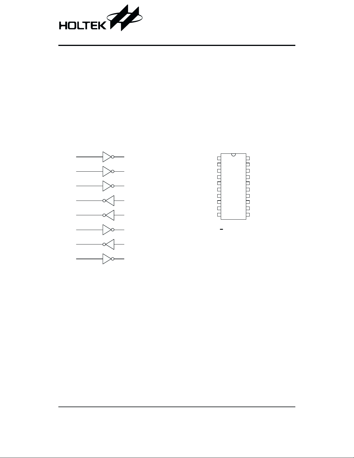
Block Diagram Pin Assignment
·
Driver current-limited output: 25mA typ.
·
Flexible supply voltage range
·
ESD protection exceeds 5kV
·
20-pin SOP package
to interface data terminal equipment (DTE) with data cir
cuit-terminating equipment (DCE).
HT6571
-
R A 1
R A 2
R A 3
D Y 1
D Y 2
R Y 1
R Y 2
R Y 3
D A 1
D A 2
V D D
R A 1
R A 2
R A 3
D Y 1
D Y 2
R A 4
D Y 3
R A 5
V S S
1
2
3
4
5
6
7
8
9
1 0
2 0
V C C
1 9
R Y 1
1 8
R Y 2
1 7
R Y 3
1 6
D A 1
1 5
D A 2
1 4
R Y 4
1 3
D A 3
1 2
R Y 5
1 1
G N D
H T 6 5 7 1
R A 4
D Y 3
R A 5
R Y 4
D A 3
R Y 5
2 0 S O P - A
Absolute Maximum Ratings
Supply Voltage (VSS VDD).......................... -15V~15V
Input Voltage Driver .......................................... 0V~7V
Output Voltage Driver .................................. -15V~15V Receiver ............................................................ 0V~7V
Supply Voltage (GND VCC)....................... -0.3V~5.5V
Receiver ...................................................... -15V~15V
Note: These are stress ratings only. Stresses exceeding the range specified under ²Absolute Maximum Ratings² may
cause substantial damage to the device. Functional operation of this device at other conditions beyond those
listed in the specification is not implied and prolonged exposure to extreme conditions may affect device reliabil
ity.
Rev. 1.20 1 August 20, 2002
-

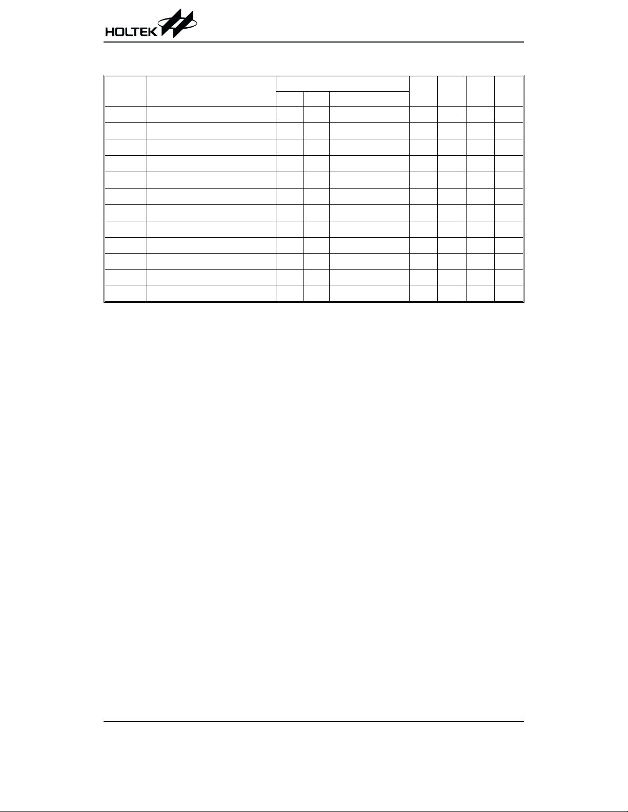
Electrical Characteristics
Symbol Paremeter
V
DD
V
SS
V
CC
V
IH1
V
IL1
V
IH2
V
IL2
I
OH1
I
OL1
I
OS(H)
I
OS(L)
S
R1
Operation Voltage
Operation Voltage
Operation Voltage
Driver Input High 12V 5V 2
Driver Input Low 12V 5V
Receiver Input High 12V 5V 3
Receiver Input Low 12V 5V
Receiver Output Source Current 12V 5V
Receiver Output Sink Current 12V 5V VO=0.4V +1 +2 +3 mA
High-level Driver Short Current 12V 5V
Low-level Driver Short Current 12V 5V VO=0V 15 25 35 mA
Slew Rate 12V 5V
Test Conditions
V
DDVCC
Conditions
¾¾ ¾
Min. Typ. Max. Unit
7.5 9 15 V
¾¾ ¾ -7.5 -9 -15
¾¾ ¾
4.5 5 5.5 V
¾¾
¾¾
¾¾
¾¾
=2.4V
V
O
=0V
V
O
=7kW,C1=330pF ¾¾
R
L
-1 -2 -3
-15 -25 -35
HT6571
V
V
0.8 V
V
0V
mA
mA
30
V/ms
Rev. 1.20 2 August 20, 2002

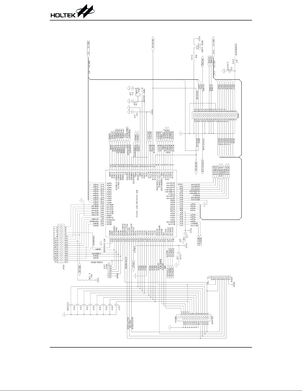
Application Circuits
HT6571
Rev. 1.20 3 August 20, 2002
 Loading...