

Keyboard Controller with PS/2
Features
•
High reliability MOS technology
•
8042-type host interface
•
6MHz-12MHz operating frequency
•
Communicates with keyboard directly
•
Provides enhanced Gate A20 switching
General Description
The HT6542B is a keyboard controller developed by Holtek with a 4-bit microprocessor . It is
pin-to-pin compatible with Intel 8042 keyboard
controller used in IBM PC’s. PC manufacturers
need not modify any printed wiring layout
when using the HT6542B in lieu of the Intel
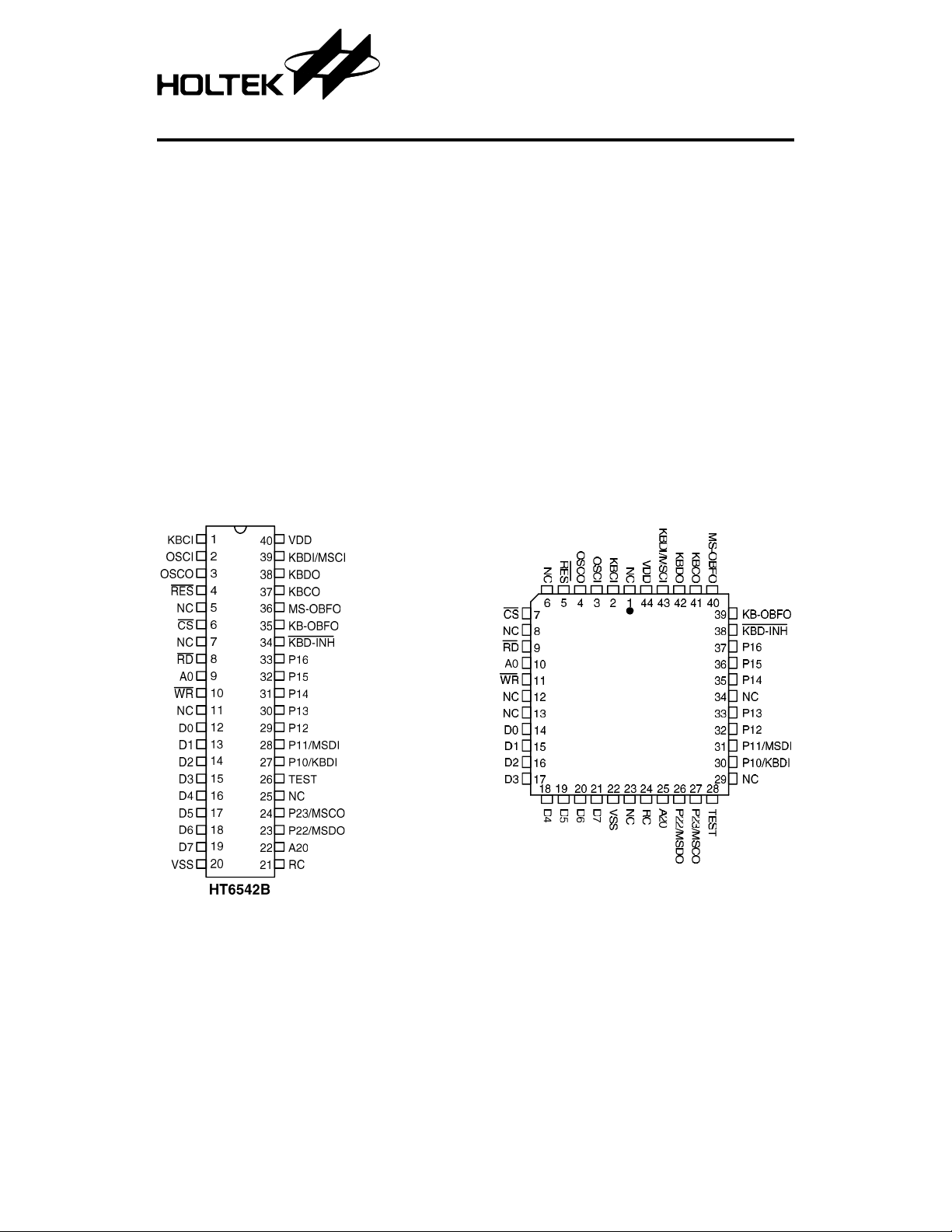
Pin Assignment
40 Pin DIP package 44 Pin PLCC package
•
Support PS/2 compatible mouse
•
Auto-detect AT and PS/2 motherboard
•
Support 40 pin DIP and 44 pin PLCC packages
8042 based keyboard controller. Furthermore,
the HT6542B can support a system clock speed
of up to 12MHz. The HT6542B can detect th e
motherboard type automatically, therefore it
can be employed on both of AT and PS/2 motherboard.
HT6542B
1 30th Nov ’95
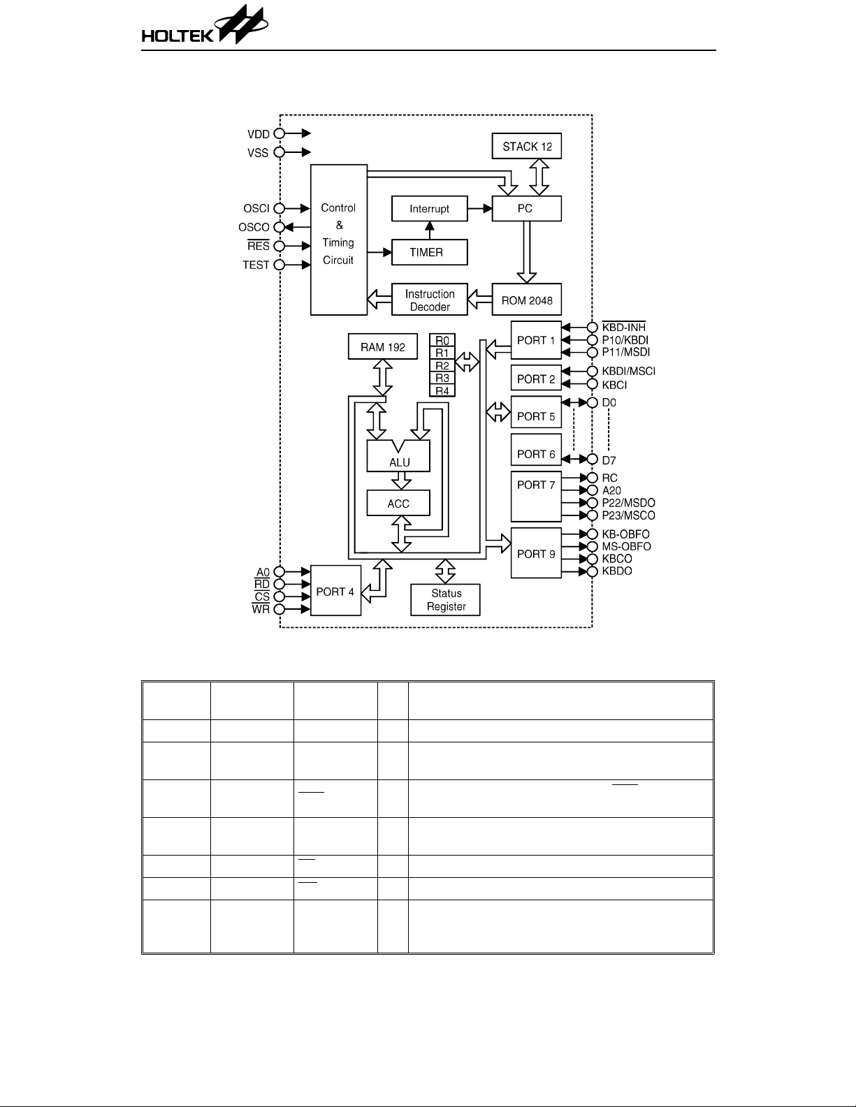
Block Diagram
HT6542B
Pin Description
Pin No.
(DIP)
1 2 KBCI I Keyboard clock input pin
2,3 3,4 OSCI,OSCO I
45
5,7,11,25
67
89
910 A0 I
Pin No.
(PLCC)
1,6,8,12,13,
23,29,34
Pin
Name
RES I
NC — No connection
CS I Host-interface chip select, active low
RD I Host-interface read signal, active low
I/O Pin Descriptions
System clock input pin, to generate internal
oscillator signal
Low level to reset HT6542B. After
level HT6542B needs 10ms to initial internal circuit
Host-interface address select input. When high, it
selects the command/sta tus registers; when low it
selects the data register
2 30th Nov ’95
RES goes to high
HT6542B
Pin No.
(DIP)
10 11 WR I Host-interface write signal, active low
12~19 14~21 D0~D7 I/O
20 22 VSS — Circuit ground
21 24 RC O Host-reset control signal output
22 25 A20 O Gate A20 control signal output
23 26 P22/MSDO I/O
24 27 P23/MSCO I/O
26 28 TEST I
27 30 P10/KBDI I/O
28 31 P11/MSDI I/O
29~33
34 38
35 39 KB-OBFO O
36 40 MS-OBFO O
37 41 KBCO O
38 42 KBDO O
39 43 KBDI/MSCI I
40 44 VDD — Positive power supply
Pin No.
(PLCC)
32~33
35~37
Pin
Name
P12~P16 I/O General purpose input/output pins
KBD-INH I
I/O Pin Descriptions
Host interface data bus. An 8-bit bi-directional port
for data transfers between the host CPU and the
HT6542B
General purpose input/output pin for AT
motherboard.
Mouse data output pin for PS/2 motherboard
General purpose input/output pin for AT
motherboard.
Mouse clock output pin for PS/2 motherboard
Test input pin, for IC test only. Connected to VCC in
applications
General purpose input/output pin for AT
motherboard.
Keyboard data input pin for PS/2 motherboard
General purpose input/output pin for AT
motherboard.
Mouse data input pin for PS/2 motherboard
Keyboard inhibit input. When low, keyboard is
inhibited. When high, keyboard transmission is
enabled.
Keyboard output buffer full interrupt for AT and
PS/2 mother board (active high)
Output low for AT mothboard.
Mouse output b uffer full interrup t for PS/2 mo ther
board (active high).
Keyboard clock output pin for AT and PS/2
motherboard.
Keyboard data output pin for AT and PS/2
motherboard.
Keyboard data input pin for AT motherboard
Mouse clock input pin for PS/2 motherboard
Absolu te Maximu m R a tin g s
Supply Voltage ............................ –0.3V to 5.5V
Input Voltage .................. V
–0.3V to VDD+0.3
SS
Storage T emperature ............... –50
Operating Temperature ................. 0
3 30th Nov ’95
°C to 125°C
°C to 70°C

D.C. Characteristics
HT6542B
Symbol Parameter
V
DD
I
DD
V
IL
V
IH
Operating Voltage — – 4.75 5 5.25 V
Operating Current 5V
Input Low Voltage — — –0.5 — 0.8 V
Input High Voltage — — 2 — V
P10~P16, KBCI, KBDI,
D0~D7, RC, A20, P22, P23,
V
OL
KB-OBFO, MS-OBFO
Output Low Voltage
I
=6mA
OL
D0~D7, KB-OBFO, MS-OBFO,
V
OH
R
PH1
R
PH2
KBCO, KBDO, A20, RC
Output High Voltage
I
=0.3mA
OH
P10~P16, KBD-INH
Pull-High Resistance
KBCI, KBDI, CS, RD, A0,
WR Pull-High Resistance
Test Condition
V
DD
Condition
=8MHz
F
OSC
No load
5V V
5V V
=0.5V — — 0.5 V
OL
=4.5V 4.5 — — V
OH
Min. Typ. Max. Unit
—4 6mA
— — 10 20 30
— — 30 50 70
DD
V
ΚΩ
ΚΩ
4 30th Nov ’95

Functional Description
Power on
When power is switched on, the HT6542B autodetect the motherboard type (AT or PS/2), then
disable the keyboard/mouse and waits for the
self-test command to perform a self-test. If no
error is detected during self-test, HEX 55 is
registered in the outp ut buffer (note that any
value other than HEX 55 would indicate
HT6542B failure) and the keyboard interface is
enabled. The HT6542B is now ready to receive
a system command or keyboard data.
Keyboard/mous e da ta transmission
The keyboard/mouse transmits data to the controller in an 11-bit format in sync, with the
keyboard/mouse clock s ignal. If this transmission is not complete d within the specified period, the HT6542B wil l register HEX FF into
the output buffer and set the "tra nsmit timeout" error bit in the STATUS REGISTER to 1.
Controller data transmission
The controller transmits data to the keyboard/mouse in the same manner as it receives
data from the keyboard/mouse. When the
HT6542B starts transmitting data and the keyboard/mouse does no t start receiving (does not
start clocking) or data transmission is not completed within 15ms , the HT65 42B will register
HEX FE into the output buffer and set the
"transmit time-out" error bit in the STATUS
REGISTER to 1.
Keyboard inhibited (KBD-INH to low)
If the KBD-INH is switched to low, the keyboard/mous e is i nhibit ed. The HT654 2B rece ive
keyboard/mouse code a nd check the
status, if inhibited the ke yboard SCAN CODE
and mouse code will be ignored and the keyboard/mouse command response is registered
into the HT6542B’s output buffer.
Status register notations
The STATUS REGIST ER is lo cated in HEX 64
of the I/O. It provides the HT6542B and interface status to the system. The following are the
definitions for each bit:
•
b0(OBF): Output buffer full
This bit is set while the HT6542B is sending
data to the output buffer and cleared when the
system reads the output buffer(I/O HEX 60H).
KBD-INH
HT6542B
•
b1(IBF): Input buffer full
This bit is set while the system is sending
data to the HT6542B’s input buffer and
cleared when th e HT6542B reads the input
buffer data.
•
b2: System flag
This bit is 0 after power-on reset, set to 1 after
self-test OK.
•
b3: Command/Data
When the system writes the data to the
HT6542B from I/O 64H, this bit becomes 1.
Reset to 0 if from I/O 60H.
•
b4:
This bit reflects the
ever data is placed in the HT65 42B’s output
buffer.
•
b5: Auxiliary Output Buffer Full.
0: The HT6542B’s output buffer is a keyboard
data.
1: The HT6542B’s output buffer is a mouse
data.
•
b6: Transmit tim e- ou t
Set to 1 when the keybo ard or mouse is not
able to completely transmite data to the
HT6542B within the specified period.
•
b7: Parity error
1: The HT6542B has received the key-
board/mouse code with a parity error.
(should be odd parity).
Outpu t buffer
The output buffer is located in I/O HEX 60. It is
used to transmi t keyboard/mouse cod e or keyboard controller response data. The output buffer data is valid only when OBF=1.
Input buffer
The input buffer is located in I/O HEX 60 or
HEX 64. The system writes command and data
into this port in the following categories:
•
Data written to I/O HEX 64 as command
write.
•
Data written to I/O HEX 60 as data write.
KBD-INH status when-
5 30th Nov ’95

Application Circuit
For AT motherboard (40 pin DIP, for example)
HT6542B
6 30th Nov ’95

For PS/2 motherboard (40 pin DIP, for example)
HT6542B
7 30th Nov ’95
 Loading...