

HT62L256
Preliminary
Features
·
Operation voltage: 2.7V~3.3V
·
Low power consumption:
-
Operating current: 20mA max.
-
Standby current: 2mA
·
High speed access time: 70ns
·
Input levels are LVTTL-compatible
General Description
The HT62L256 is a 262,144-bit static random access
memory organized into 32,768 words by 8 bits and oper
ating from a low power range of 2.7V to 3.3V supply volt
age. It is fabricated with high performance CMOS
process that provides both high speed and low power
feature with typical standby current of 2mA and maxi
mum access time of 70ns.
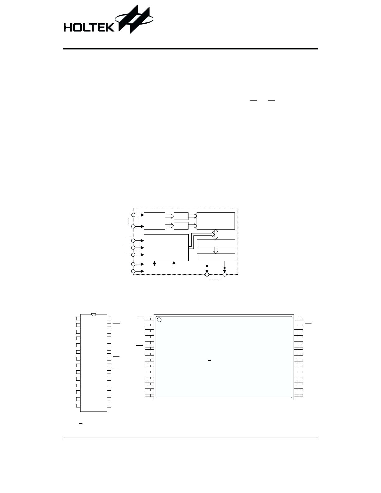
Block Diagram
A 1 4
A 0
A d d r e s s
B u f f e r s
X - D e c
Y - D e c
CMOS 32K´8 Low Power SRAM
·
Automatic power down when chip is deselected
·
Three state outputs
·
Fully static operation
·
Data retention supply voltage as low as 2.0V
·
Easy expansion with CS and OE options
·
28-pin SOP/TSOP package
The HT62L256 has an automatic power down feature,
reducing the power consumption significantly when chip
is deselected. The HT62L256 supports the JEDEC
standard 28-pin SOP and TSOP package.
-
M e m o r y C e l l A r r a y
( 3 2 K
8 B i t s
´
Pin Assignment
A 1 4
A 1 2
A 7
A 6
A 5
A 4
A 3
A 2
A 1
A 0
D 0
D 1
D 2
V S S
1
2
3
4
5
6
7
8
9
1 0
1 1
1 2
1 3
1 4
H T 6 2 L 2 5 6
2 8 S O P - A
2 8
2 7
2 6
2 5
2 4
2 3
2 2
2 1
2 0
1 9
1 8
1 7
1 6
1 5
V D D
W E
A 1 3
A 8
A 9
A 1 1
O E
A 1 0
C S
D 7
D 6
D 5
D 4
D 3
V D D
V S S
C S
W E
O E
A 1 1
A 1 3
W E
V D D
A 1 4
A 1 2
O E
A 9
A 8
A 7
A 6
A 5
A 4
A 3
R e a d / W r i t e
C o n t r o l L o g i c
1
1 4
S e n s e A m p l i f i e r
O u t p u t B u f f e r s
D 0 D 7
H T 6 2 L 2 5 6
2 8 T S O P - A
2 8
1 5
A 1 0
C S
D 7
D 6
D 5
D 4
D 3
V S S
D 2
D 1
D 0
A 0
A 1
A 2
Rev. 0.00 1 August 15, 2002
Preliminary
HT62L256
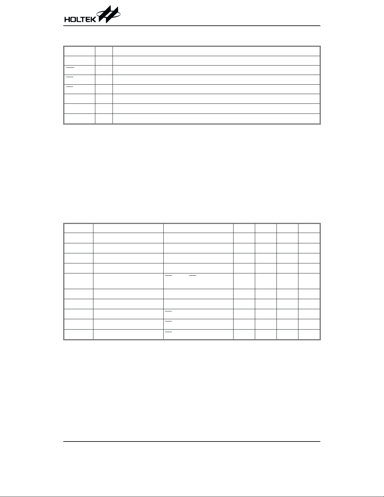
Pin Description
Pin Name I/O Description
A0~A14 I Address input pins
WE
OE
CS
I Write enable signal pin, active LOW
I Output enable signal pin, active LOW
I Chip select signal pin, active LOW
D0~D7 I/O Data input and output signal pins
VDD
VSS
Positive power supply
¾
Negative power supply, ground
¾
Absolute Maximum Rating
VDDto VSS ........................................... -0.5V to +3.6V
IN, IN/OUT Voltage to V
............. -0.5V to VDD+0.5V
SS
Operating Temperature, T
Storage Temperature (Plastic), Tstg ... -55°Cto125°C
Power Consumption, PT .......................................0.7W
Note: These are stress ratings only. Stresses exceeding the range specified under ²Absolute Maximum Ratings² may
cause substantial damage to the device. Functional operation of this device at other conditions beyond those
listed in the specification is not implied and prolonged exposure to extreme conditions may affect device reliabil
ity.
......................0°Cto70°C
OP
-
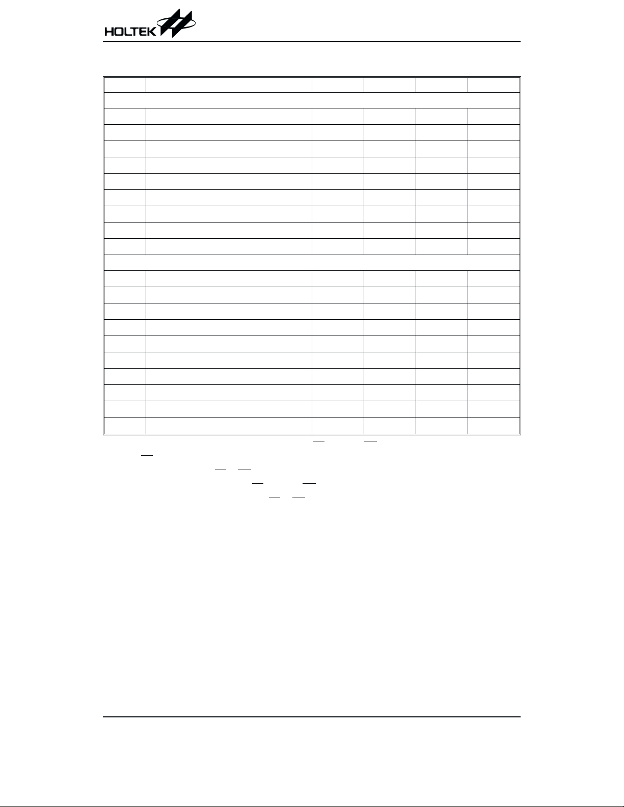
D.C. Characteristics
Ta=25°C, VDD=3.0V±10%, TOP=0°Cto70°C
Symbol Parameter Test Conditions Min. Typ. Max. Unit
I
I
I
V
V
V
I
LI
I
LO
V
V
DD
SB1
SB2
DD
IL
IH
OL
OH
Operating Voltage
Input Low Voltage
Input High Voltage
Input Leakage Current
Output Leakage Current
Output Low Voltage
Output High Voltage
Operating Current
Standby Current
Power Down Supply Current
¾
¾¾
¾ 0.7´V
=0 to V
V
CS
V
V
V
CS
CS
CS
IN
OUT
DD
DD
DD
=VIHor OE=VIH,
=0 to V
DD
=Max, IOL=2mA
=Min, IOH=-1mA VDD-0.3 ¾¾
=VIH,I
=VIH,I
OUT
OUT
=0mA
=0mA
³ VDD- 0.2V, VIN³0V ¾
2.7 3.0 3.3 V
0 0.4 V
DD
¾¾
¾¾
¾¾
0.3 V
¾¾
¾¾
210
¾
1
1
20 mA
50
V
mA
mA
V
mA
mA
Rev. 0.00 2 August 15, 2002
Preliminary
HT62L256
A.C. Characteristics
Ta=25°C, VDD=3.0V±10%
Symbol Parameter Min. Typ. Max. Unit
Read cycle
t
RC
t
AA
t
ACS
t
AOE
t
CLZ*
t
OLZ
t
CHZ
t
OHZ
t
OH
Read Cycle Time 70
Address Access Time
Chip Selection Access Time
Output Enable to Valid Outputs
Chip Selection to Output in Low-Z 10
*
Output Enabled to Output in Low-Z 5
*
Chip Deselected to Output in High-Z
*
Output Disable to Output in High-Z
Output Hold from Address Change 10
¾¾
¾¾
¾¾
¾¾
¾¾
¾¾
¾¾
¾¾
¾¾
70 ns
70 ns
35 ns
25 ns
25 ns
Write cycle
t
WC
t
CW
t
AS
t
AW
t
WP
t
WR
t
WHZ
t
DW
t
DH
t
OW
Write Cycle Time 70
Chip Selection to End of Write 60
Address Setup Time 0
Address Valid to End of Write 60
Write Pulse Width 50
Write Recovery Time 0
¾¾
¾¾
¾¾
¾¾
¾¾
¾¾
Write to Output in High-Z ¾¾
Data Valid to End of Write 30
Data Hold from End of Write 0
Output Active from End of Write 5
¾¾
¾¾
¾¾
20 ns
ns
ns
ns
ns
ns
ns
ns
ns
ns
ns
ns
ns
ns
Note: 1. A write cycle occurs during the overlap of a low CS and a low WE
2. OE may be both high and low in a write cycle
is specified from CS or WE, whichever occurs last
3. t
AS
is an overlap time of a low CS and a low WE
4. t
WP
5. tWR,tDWand tDHare specified from CS or WE, whichever occurs first
is specified by the time when DATA OUT is floating and not defined by the output level
6. t
WHZ
7. When the I/O pins are in data output mode, they should not be forced with inverse signals
Rev. 0.00 3 August 15, 2002
Preliminary
A.C. Test Conditions
Item Conditions
Input Pulse Level 0V to 3V
Input Rise and Fall Time 5ns
Input and Output Timing Reference Level 1.5V
Output Load See figures below
HT62L256
+ 1 . 5 V
1 . 8 k
W
I / O
9 9 0
W
* I n c l u d i n g s c o p e a n d j i g
1 0 0 p F
+ 1 . 5 V
1 . 8 k
W
I / O
9 9 0
W
* I n c l u d i n g s c o p e a n d j i g
5 p F
O u t p u t l o a d O u t p u t l o a d f o r
t C L Z , t O L Z , t C H Z , t W H Z a n d t O W
Functional Description
Operation truth table
CS
H X X Standby High-Z
L H H Output Disable High-Z
L L H Read Dout
L X L Write Din
Data retention characteristics
Symbol Parameter Conditions Min. Max. Unit
V
DR
I
CCDR
t
CDR
t
R
VDDfor Data Retention
Data Retention Current
Chip Disable Data Retention Time See retention timing 0
Operation Recovery Time See retention timing
OE WE Mode D0~D7
Ta =-40°Cto85°C
CS
³ VDD-0.2V
V
³ VDD-0.2V or VIN£0.2V
IN
³ VDD-0.2V
CS
V
³ VDD-0.2V or VIN£0.2V
IN
2.0 3.3 V
¾
2
¾
*
t
RC
¾
mA
ns
ns
Low VDDdata retention timing
V
D D
C S
3 . 0 V
3 . 0 V
V
2 . 0 V
D D
³
t
C D R
V
I H
C S
V
- 0 . 2 V
³
D D
t
R
V
I H
Rev. 0.00 4 August 15, 2002

Timing Diagrams
Read cycle 1 output enable controlled (1)
A d d r e s s
t
A A
O E
t
A O E
t
O L Z
C S
t
A C S
t
C L Z
D
O U T
Preliminary
t
R C
HT62L256
t
O H
t
O H Z
t
C H Z
D o n ' t C a r e
U n u s e d
Read cycle 2 address controlled (1, 2, 4)
t
R C
A d d r e s s
t
A A
t
O H
D
O U T
Read cycle 3 chip select controlled (1, 3, 4)
A d d r e s s
t
A C S
t
C L Z
D
O U T
Note: 1. WE
is high for read cycle
2. Device is continuously enabled, CS
=V
IL
3. Address is valid prior to or coincident with the CS transition low
=V
4. OE
IL
5. Transition is measured at ±500mV from the steady state
t
O H
t
D o n 't C a r e
U n u s e d
C H Z
D o n 't C a r e
U n u s e d
Rev. 0.00 5 August 15, 2002

Write cycle 1 OE clock (1)
A d d r e s s
O E
Preliminary
t
W C
t
W R
t
C W
HT62L256
C S
W E
D
O U T
D
I N
Write cycle 2 OE
A d d r e s s
C S
W E
D
O U T
t
A S
t
O H Z
=VILFixed (1, 6)
t
A S
( 5 )
t
A W
t
W P
( 1 , 4 )
t
t
D W
D H
D o n ' t C a r e
U n u s e d
t
W C
t
C W
t
W R
( 5 )
t
A W
t
W P
t
O H
t
W H Z
t
O W
( 7 ) ( 8 )
t
D
I N
t
D W
D H
D o n ' t C a r e
U n u s e d
Rev. 0.00 6 August 15, 2002

Preliminary
Note: 1. WE must be high during all address transitions
2. A write occurs during the overlap (t
3. tWRis measured from the earliest high going edge of CS or WE to the end of the write cycle
4. During this period, I/O pins are in the output state, so the input signals of opposite phase to the outputs
should not be applied.
5. If the CS
high impedance state
6. OE
7. D
8. D
9. If CS is low during this period, then the I/O pins are in the output state and the data input signals of the
opposite phase to the outputs should not be applied
10. Transition is measured at ±500mV from the steady state
low transition occurs simultaneously or after with the WE low transition, the outputs remain in a
is continuously low (OE=VIL)
is at the same phase as the write data of this write cycle
OUT
is the read data of the next address
OUT
) of a low CS and a low WE
WP
HT62L256
Rev. 0.00 7 August 15, 2002

Package Information
28-pin SOP (330mil) outline dimensions
Preliminary
HT62L256
2 8
A
1
C
C '
D
E
Symbol
A 453
B 326
C14
C¢
D92
E
F4
G32
H4
a 0°¾10°
1 5
B
1 4
G
H
F
Dimensions in mil
Min. Nom. Max.
700
¾
=
¾
¾
¾
¾
¾
50
¾¾
¾
¾
477
336
20
728
104
¾
38
12
Rev. 0.00 8 August 15, 2002

28-pin TSOP (8´13.4) outline dimensions
H
D
1
Preliminary
2 8
HT62L256
D e t a i l F
¾
¾
0.20
¾
¾
¾
0.55
0.50
0.8
G
L
bS
y
1 4 1 5
D
S e e D e t a i l F
Symbol
A
A1 0.08
A2 0.95
b
D 11.70
H
D
E 7.90
e
L
L1
E
0 . 0 1 0
L 1
S e a t i n g P l a n e
Dimensions in mm
Min. Nom. Max.
¾¾
¾
13.20
¾
¾
¾
q 0°¾5°
A 2
A
A 1
e
1.25
0.18
1.05
¾
11.90
13.60
8.10
¾
¾
¾
Rev. 0.00 9 August 15, 2002

Product Tape and Reel Specifications
Reel dimensions
Preliminary
HT62L256
T 2
A
B
T 1
SOP 28E (330mil)
Symbol Description Dimensions in mm
A Reel Outer Diameter
B Reel Inner Diameter
C Spindle Hole Diameter
D Key Slit Width
T1 Space Between Flange
T2 Reel Thickness
D
330±1.0
62±1.5
13.0+0.5
2.0±0.5
24.8+0.3
30.2±0.2
C
-0.2
-0.2
Rev. 0.00 10 August 15, 2002

Carrier tape dimensions
Preliminary
HT62L256
D
E
F
PD 1
SOP 28E (330mil)
Symbol Description Dimensions in mm
W Carrier Tape Width
P Cavity Pitch
E Perforation Position
F Cavity to Perforation (Width Direction)
D Perforation Diameter 1.55+0.1
D1 Cavity Hole Diameter 1.5+0.25
P0 Perforation Pitch
P1 Cavity to Perforation (Length Direction)
A0 Cavity Length
B0 Cavity Width
K0 Cavity Depth
t Carrier Tape Thickness
C Cover Tape Width 21.3
P 1P 0
W
A 0
B 0
C
24.0+0.3
16.0±0.1
1.75±0.1
11.5±0.1
4.0±0.1
2.0±0.1
12.32±0.1
18.8±0.1
3.0±0.1
0.3±0.05
t
K 0
-0.1
Rev. 0.00 11 August 15, 2002

Preliminary
HT62L256
Holtek Semiconductor Inc. (Headquarters)
No.3, Creation Rd. II, Science-based Industrial Park, Hsinchu, Taiwan
Tel: 886-3-563-1999
Fax: 886-3-563-1189
http://www.holtek.com.tw
Holtek Semiconductor Inc. (Sales Office)
11F, No.576, Sec.7 Chung Hsiao E. Rd., Taipei, Taiwan
Tel: 886-2-2782-9635
Fax: 886-2-2782-9636
Fax: 886-2-2782-7128 (International sales hotline)
Holtek Semiconductor (Shanghai) Inc.
7th Floor, Building 2, No.889, Yi Shan Rd., Shanghai, China
Tel: 021-6485-5560
Fax: 021-6485-0313
http://www.holtek.com.cn
Holtek Semiconductor (Hong Kong) Ltd.
RM.711, Tower 2, Cheung Sha Wan Plaza, 833 Cheung Sha Wan Rd., Kowloon, Hong Kong
Tel: 852-2-745-8288
Fax: 852-2-742-8657
Holmate Semiconductor, Inc.
48531 Warm Springs Boulevard, Suite 413, Fremont, CA 94539
Tel: 510-252-9880
Fax: 510-252-9885
http://www.holmate.com
Copyright Ó 2002 by HOLTEK SEMICONDUCTOR INC.
The information appearing in this Data Sheet is believed to be accurate at the time of publication. However, Holtek as
sumes no responsibility arising from the use of the specifications described. The applications mentioned herein are used
solely for the purpose of illustration and Holtek makes no warranty or representation that such applications will be suitable
without further modification, nor recommends the use of its products for application that may present a risk to human life
due to malfunction or otherwise. Holtek reserves the right to alter its products without prior notification. For the most
up-to-date information, please visit our web site at http://www.holtek.com.tw.
-
Rev. 0.00 12 August 15, 2002
 Loading...