Holtek Semiconductor Inc HT6247, HT640, HT6187 Datasheet

Features
Operating voltage: 2.4V~12V
·
Low power and high noise immunity CMOS
·
technology
Low standby current
·
Three words transmission
·
Applications
Burglar alarm system
·
Smoke and fire alarm system
·
Garage door controllers
·
Car door controllers
·
General Description
The 318encoders are a series of CMOS LSIs for
remote control system applications. They are
capable of encoding 18 bits of information
which consists of N address bits and 18-N data
bits. Each address/data input is externally
trinary programmable if bonded out. It is otherwise set floating internally. Various packages of
18
the 3
encoders offer flexible combinations of
18
3
Series of Encoders
Built-in oscillator needs only 5% resistor
·
Easy interface with an RF or infrared trans
·
mission media
Minimal external components
·
Car alarm system
·
Security system
·
Cordless telephones
·
Other remote control systems
·
programmable address/data to meet various
application needs. The programmable ad
dress/data is transmitted together with the
header bits via an RF or an infrared transmis
sion medium upon receipt of a trigger signal.
The capability to select a TE trigger type or a
DATA trigger type further enhances the application flexibility of the 3
18
series of encoders.
-
-
-
Selection Table
Function
Part No.
HT600 9 5 0 4 RC oscillator TE 20 DIP/20 SOP
HT640 10 8 0 0 RC oscillator TE 24 SOP/24 SDIP
HT680 8 4 0 6 RC oscillator TE 18 DIP
HT6187 9 0 3 6 RC oscillator D12,D14,D15 18 DIP/20 SOP
HT6207 10 0 4 4 RC oscillator D12~D15 20 DIP/20 SOP
HT6247 12 0 6 0 RC oscillator D12~D17 24 SOP/24 SDIP
Note: Address/Data represents addressable pins or data according to the decoder requirements.
Address
No.
Address/
Data No.
Data
No.
Dummy
Code No.
1 July 8, 1999
Oscillator Trigger Package

318Series of Encoders
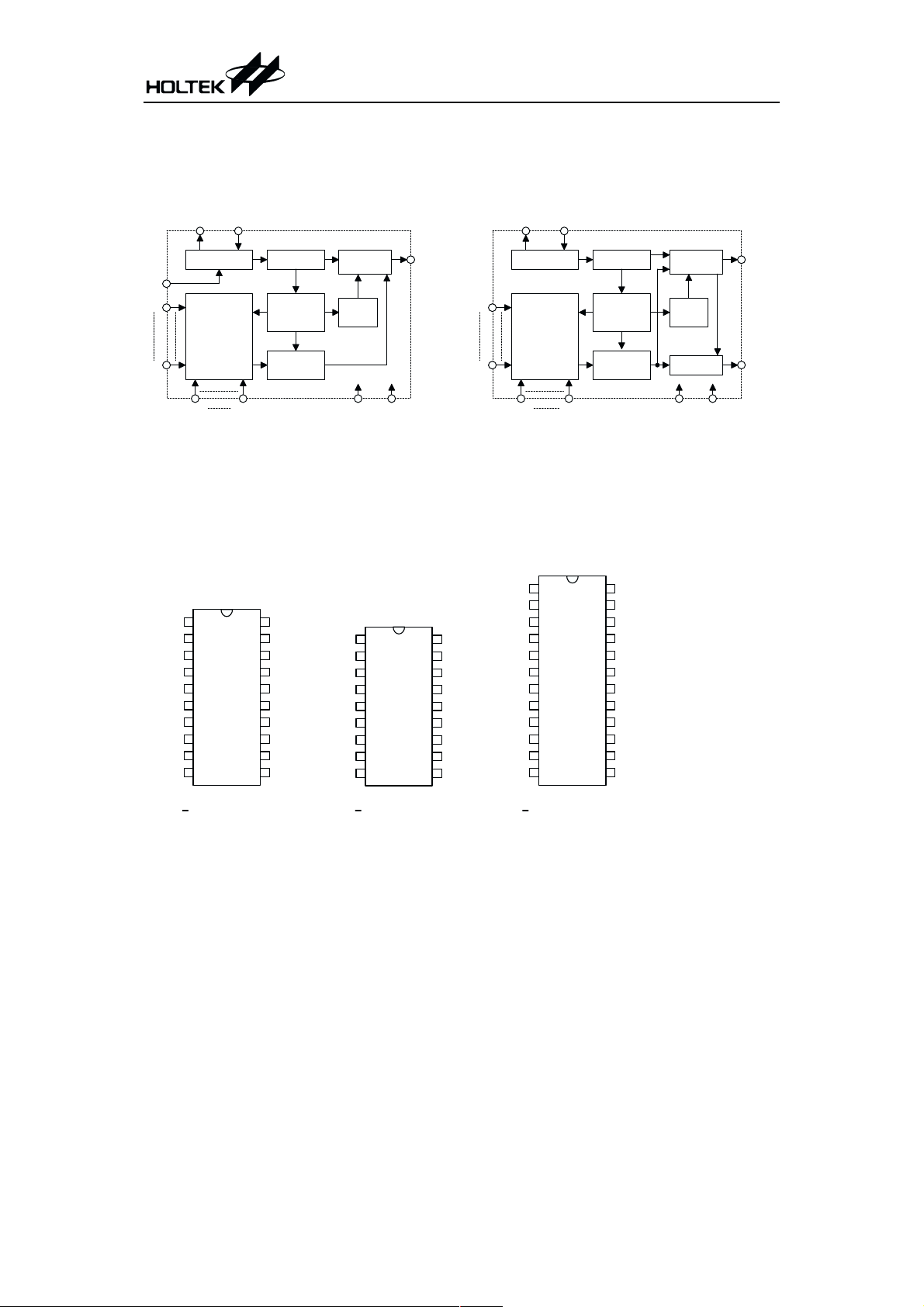
Block Diagram
TE trigger DATA trigger
HT600/HT640/HT680 HT6187/HT6207/HT6247
OSC2
OSC1
OSC2
OSC1
O scillator
TE
A0
18
Transm ission
Gate Circuit
A9
AD10
AD17
33 Divider
¸
18 C ounter
¸
& 1 of 18
D ecoder
Trinary
Detector
D ata Select
& Buffer
Sync.
Circuit
VDD VSS
DOUT
O scillator
A0
18
Transm ission
Gate Circuit
A11
D12
Note: The address/data pins are available in various combinations.
Pin Assignment
TE trigger type
9-A ddress
5 -A d d re s s /D a ta
1
AD11
2
AD12
3
AD13
4
AD14
5
AD15
DOUT
OSC2
OSC1
TE
VSS
6
7
8
9
10
HT600
20 D IP /S O P
8-A ddress
4-A d dress/D ata
VDD
20
19
A9
18
A8
17
A7
16
A6
A4
15
A3
14
A2
13
A1
12
11
A0
AD11
AD12
AD14
AD15
DOUT
TE
OSC2
OSC1
VSS
1
2
3
4
5
6
7
8
9
18
17
16
15
14
13
12
11
10
HT680
18 D IP /S O P
10-A ddress
8-A d dress/D ata
AD11
AD12
AD13
VDD
A9
A8
A7
A6
A3
A2
A1
A0
AD14
AD15
AD16
AD17
DOUT
OSC2
OSC1
1
2
3
4
5
6
7
8
TE
9
10
11
VSS
12
24 SOP/SDIP
D17
HT640
33 Divider
¸
18 C ounter
¸
& 1 of 18
D ecoder
Trinary
Detector
24
23
22
21
20
19
18
17
16
15
14
13
VDD
AD10
A9
A8
A7
A6
A5
A4
A3
A2
A1
A0
D ata Select
& Buffer
Sync.
Circuit
LED Circuit
VDD VSS
DOUT
LED
2 July 8, 1999

DATA trigger type
318Series of Encoders
VDD
A9
A8
A7
A6
A4
A3
A2
A1
A0
12-A dd ress
6 -D a ta
DOUT
OSC2
OSC1
9-A ddress
3 -D a ta
A11
1
2
D12
D14
3
4
D15
5
DOUT
LED
6
OSC2
7
OSC1
8
VSS
9
H T 6187
18 D IP
9 -A d d r e s s
3 -D a ta
18
VDD
17
A9
A8
16
15
A7
14
A6
A3
13
A2
12
A1
11
A0
10
NC
A11
D12
D14
D15
DOUT
LED
OSC2
OSC1
VSS
19
2
18
3
17
4
16
5
15
6
14
7
13
8
12
9
11
10
20
1
H T 6187
20 S O P
NC
VDD
A9
A8
A7
A6
A3
A2
A1
A0
10-A ddress
4 -D a ta
A11
1
2
D12
3
D13
4
D14
5
D15
DOUT
6
LED
7
8
OSC2
OSC1
9
10
VSS
H T 6207
20 DIP/SO P
20
19
18
17
16
15
14
13
12
11
Pin Description
Pin Name I/O
A0~A11 I
AD10~AD17 I
D12~D17 I
DOUT O CMOS OUT Encoder data serial transmission output
LED O NMOS OUT LED transmission enable indicator
TE I
OSC1 I OSCILLATOR Oscillator input pin
OSC2 O OSCILLATOR Oscillator output pin
VSS I
VDD I
Internal
Connection
TRANSMISSION
GATE
TRANSMISSION
GATE
CMOS IN
Pull-low
CMOS IN
Pull-low
¾
¾
Description
Input pins for address A0~A11 setting
They can be externally set to VDD, VSS, or left open.
Input pins for address/data (AD10~AD17) setting
They can be externally set to VDD, VSS, or left open.
Input pins for data (D12~D17) setting and transmission
enable (active high)
They an be externally set to VDD or left open (see Note).
Transmission enable, active high (see Note).
Negative power supply (GND)
Positive power supply
A11
1
2
D12
3
D13
4
D14
5
D15
D16
6
D17
7
8
LED
9
10
11
VSS
12
H T 6247
24 SOP/SDIP
24
VDD
23
A10
22
A9
21
A8
20
A7
A6
19
A5
18
A4
17
16
A3
15
A2
A1
14
A0
13
Notes: D12~D17 are data input and transmission enable pins of the HT6187/HT6207/HT6247.
TE is the transmission enable pin of the HT600/HT640/HT680.
3 July 8, 1999

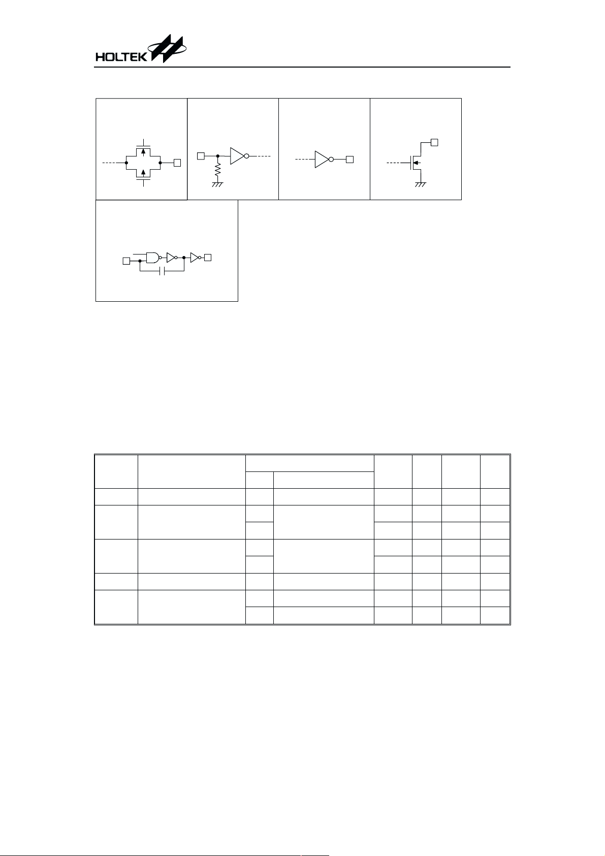
Approximate internal connection circuits
318Series of Encoders
TRANSM ISSION
GATE
OSCILLATOR
EN
OSC1
CMOS IN
Pull-low
OSC2
CMOS OUT
NMOS OUT
Absolute Maximum Ratings
Supply Voltage...............................-0.3V to 13V
Storage Temperature.................-50°Cto125°C
Note: These are stress ratings only. Stresses exceeding the range specified under ²Absolute Maxi-
mum Ratings² may cause substantial damage to the device. Functional operation of this device at other conditions beyond those listed in the specification is not implied and prolonged
exposure to extreme conditions may affect device reliability.
Input Voltage ...................V
-0.3 to VDD+0.3V
SS
Operating Temperature ..............-20°Cto75°C
Electrical Characteristics
Symbol Parameter
V
DD
I
STB
I
DD
I
LED
I
DOUT
Operating Voltage
Standby Current
Operating Current
LED Sink Current 5V
Output Drive Current
Test Conditions
V
DD
Conditions
¾¾
3V
Oscillator stops
12V
5V
No load
=100kHz
f
OSC
12V
V
=0.5V
LED
V
5V
5V
=0.9VDD(Source)
OH
V
=0.1VDD(Sink)
OL
4 July 8, 1999
Ta=25°C
Min. Typ. Max. Unit
2.4
¾
¾
¾
¾
¾
0.1 1
24
250 500
1200 2400
1.5 3
-0.6 -1.2 ¾
0.6 1.2
12 V
mA
mA
mA
mA
¾
mA
mA
¾
mA
 Loading...