Multi-Purpose Encoders
Features
Operating voltage: 1.8V~3.5V
·
DOUT with 38kHz carrier for IR medium
·
Low standby current
·
Minimum transmission word: one word
·
455kHz ceramic resonator or crystal
·
16-bit address codes
·
8-bit data codes
·
Applications
Television and video cassette recorder con
·
trollers
Burglar alarm systems
·
Smoke and fire alarm systems
·
Garage door controllers
·
General Description
The HT6221/HT6222 are CMOS LSI encoders
designed for use in remote control systems. They
are capable of encoding 16-bit address codes and
8-bit data codes. Each address/data input can be
set to one of the two logic states, 0 and 1.
HT6221/HT6222
PPM code method
·
Three double-active keys
·
Maximum active keys
·
-
HT6221: 32 keys
-
HT6222: 64 keys
Low power and high noise immunity
·
CMOS technology
Car door controllers
·
Car alarm systems
·
Security systems
·
Other remote control systems
·
The HT6221/HT6222 contain 32 keys
(K1~K32) and 64 keys (K1~K64), respectively.
When one of the keys is triggered, the programmed address/data is transmitted together
with the header bits via an IR (38kHz carrier)
transmission medium.
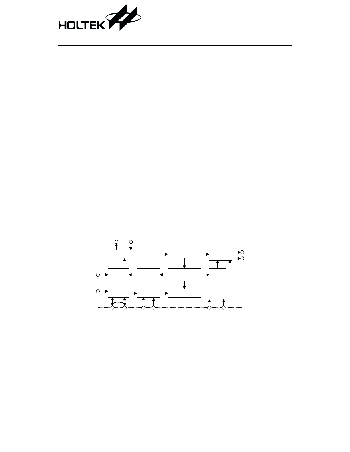
Block Diagram
R1
R8
X2 X1
O scillator D ivider
24 C ounter &
Keyboard
Matrix &
Gate
Circuit
C1 C8 AIN D7
Data ROM
& R egisters
¸
1 of 24 D ecoder
Binary D etector
1 March 2, 2000
D ata S elect
& Buffer
Sync.
Circuit
VDD VSS
DOUT
LED

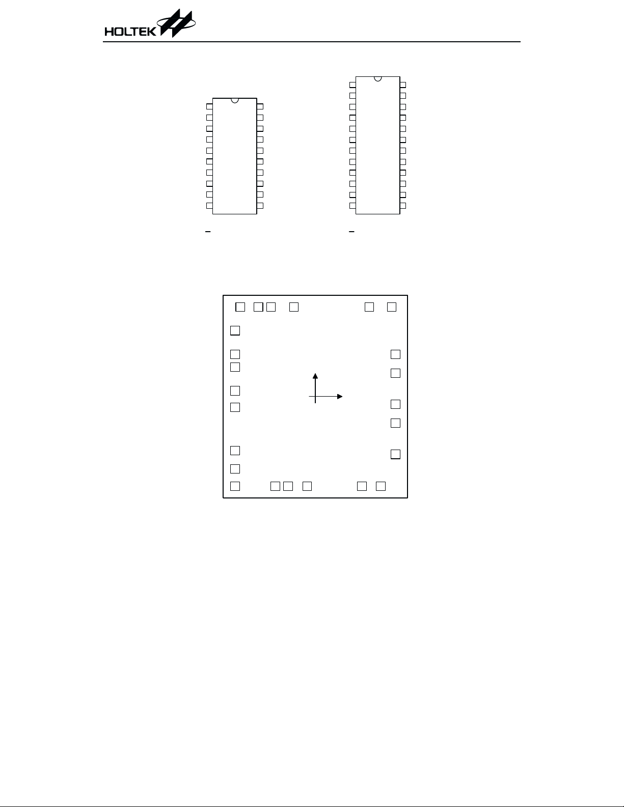
Pin Assignment
Pad Assignment
R1
R2
R3
R4
DOUT
VDD
D7
X2
X1
VSS
20
1
19
2
18
3
17
4
16
5
15
6
14
7
13
8
12
9
11
10
H T6221
20 D IP/SOP
KI2
KI3
AIN
C1
C2
C3
C4
C5
C6
C7
C8
LED
KI1
HT6221/HT6222
1
R3
2
R4
3
R5
4
R6
5
R7
6
R8
VDD
D7
X2
X1
VSS
7
8
9
10
11
12
DOUT
24 D IP /S O P
KI0
H T6222
CCS
24
R2
23
R1
22
AIN
21
C1
20
C2
19
C3
18
C4
17
C5
16
C6
15
C7
14
C8
13
LED
KIO 0
19
KIO 1
18
KIO 2
17
16
KIO 3
15
KIO 4
14
KIO 5
KI4
KI5
KI6
KI7
REM
VDD
SEL
OSCO
23
24
1
2
3
4
5
6
7
8
21
22
9
10
OSCI
VSS
Chip size: 94 ´ 104 (mil)
20
(0 ,0 )
11
LM B
13
12
KIO 6
KIO 7
2
* The IC substrate should be connected to VDD in the PCB layout artwork.
2 March 2, 2000

HT6221/HT6222
Pad Coordinates Unit: mil
Pad No. X Y Pad No. X Y
1
2
3
4
5
6
7
8
9
10
11
12 24.31
-41.99
-41.99
-41.99
-41.99
-41.99 -5.61
-41.99 -28.31
-41.99 -37.83
-41.99 -46.88
-20.95 -46.88
-14.32 -46.88
-4.25 -46.88
Pin Description
HT6222
Pin No. Pin Name I/O
1~6 R3~R8 I
7 DOUT O CMOS OUT Serial data output pin, with a 38kHz carrier
8 VDD
9 D7 I CMOS IN Most significant data bit (D7) code setting
10 X2 O OSCILLATOR 455kHz resonator oscillator output
11 X1 I OSCILLATOR 455kHz resonator oscillator input
12 VSS
13 LED O CMOS OUT Transmission enable indicator output
14~21 C8~C1 I/O
22 AIN I
23~24 R1~R2 I
34.43 13 34.17
22.02 14 41.95
15.39 15 41.95
2.98 16 41.95
17 41.95 12.16
18 41.95 22.02
19 39.99 46.84
20 28.26 46.84
21
22
23
-46.88
Connection
¾¾
¾¾
CMOS IN/OUT
24
Internal
CMOS IN
Pull-low
Pull-low
CMOS IN
Pull-high
Pull-low
CMOS IN
Pull-low
-11.18
-23.16
-29.79
-39.27
Row control for keyboard matrix, active high
Positive power supply, 1.8V~3.5V for normal
operation
Negative power supply
Column control for keyboard matrix
Low byte address codes (8 bits) scan input
Row control for keyboard matrix, active high
-46.88
-30.26
-13.98
-4.12
46.84
46.84
46.84
46.84
Description
3 March 2, 2000

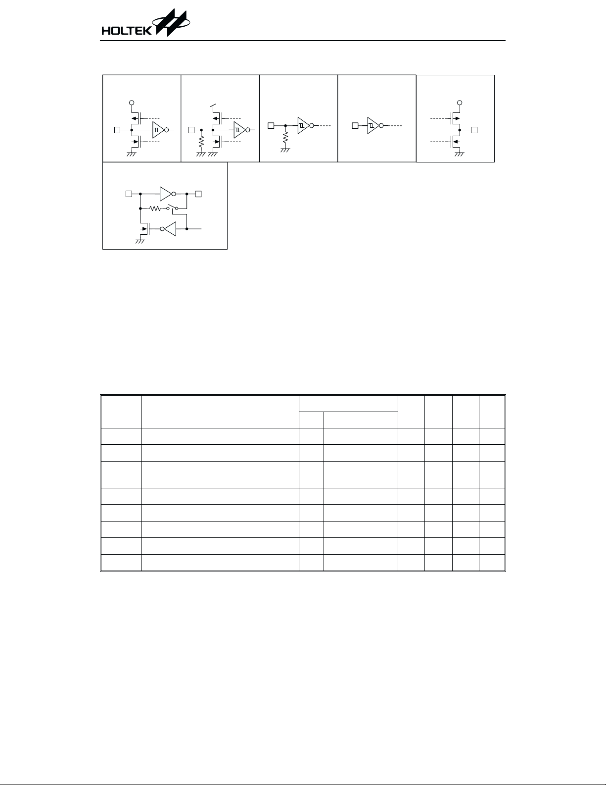
Approximate internal connection circuits
HT6221/HT6222
CMOS IN/O UT
V
DD
OSCILLATOR
X1
10M
W
CMOS IN/O UT
Pull-low
X2
EN
CMOS IN
Pull-low
CMOS IN
CMOS OUT
V
DD
Absolute Maximum Ratings
Supply Voltage.................................-0.3V to 6V
Input Voltage .................V
-0.3V to VDD+0.3V
SS
Note: These are stress ratings only. Stresses exceeding the range specified under "Absolute Maxi
mum Ratings" may cause substantial damage to the device. Functional operation of this device
at other conditions beyond those listed in the specification is not implied and prolonged exposure to extreme conditions may affect device reliability.
Storage Temperature.................-50°Cto125°C
Operating Temperature ..............-20°Cto75°C
-
Electrical Characteristic
Symbol Parameter
V
I
I
I
I
I
I
I
STB
DD
OH1
OL1
OH2
OL2
OH3
Operating Voltage
DD
Standby Current 3V Oscillator stops
Operating Current 3V
Output Source Current for DOUT 3V
Output Sink Current for DOUT 3V
Output Source Current for LED 3V
Output Sink Current for LED 3V
Output Source Current for C1~C8 3V
Ta=25°C
Test Conditions
Min. Typ. Max. Unit
V
4 March 2, 2000
Conditions
DD
¾¾
=455kHz
f
OSC
No load
V
=2.7V
O
V
=0.3V
O
V
=2.7V
O
V
=0.3V
O
V
=2.7V
O
1.8 3 3.5 V
0.1 1.0
¾
200 400
¾
-2.0 -4.0 ¾
50 100
mA
mA
mA
¾mA
-10 -60 ¾mA
1.2 2.0
-0.6 -2.0 ¾
¾
mA
mA
 Loading...