Holtek Semiconductor Inc HT6010, HT6012, HT6014 Datasheet

Features
Operating voltage: 2.4V~12V
·
Low power and high noise immunity CMOS
·
technology
Low standby current
·
Minimum transmission word
·
-
Four words for TE trigger
-
One word for Data trigger
Applications
Burglar alarm system
·
Smoke and fire alarm system
·
Garage door controllers
·
Car alarm system
·
General Description
The 312encoders are a series of CMOS LSIs for
remote controlsystem applications. They are ca
pable of encoding 12 bits of information which
consists of N address bits and 12-N data bits.
Each address/data input is externally trinary
programmable if bonded out.They are otherwise
set floating internally. Various packages of the
12
3
encoders offer flexible combinations of
12
3
-
Series of Encoders
Built-in oscillator needs only 5% resistor
·
Easy interface with an RF or an infrared
·
transmission medium
Minimal external components
·
Package information: refer to Selection
·
Table
Security system
·
Cordless telephones
·
Other remote control systems
·
programmable address/data which meet vari
ous applications. The programmable ad
dress/data is transmitted together withthe header
bits via an RFor an infrared transmissionmedium
upon receipt of a trigger signal. A TE
a DATA (HT6012/HT6014) trigger can be selectedforapplicationflexibility.
-
-
(HT6010) or
Selection Table
Function
Part No.
HT6010 8 4 0 RC oscillator TE
HT6012 10 0 2 RC oscillator D10~D11 Yes 18 DIP/20 SOP
HT6014 8 0 4 RC oscillator D8~D11 Yes 18 DIP/20 SOP
Note: Address/Data represents addressable pins or data according to the requirements of decoders.
Address
No.
Address/
Data No.
Data
No.
Oscillator Trigger
1 December 13, 1999
LED
Indicator
No
Package
18/20 DIP
20 SOP

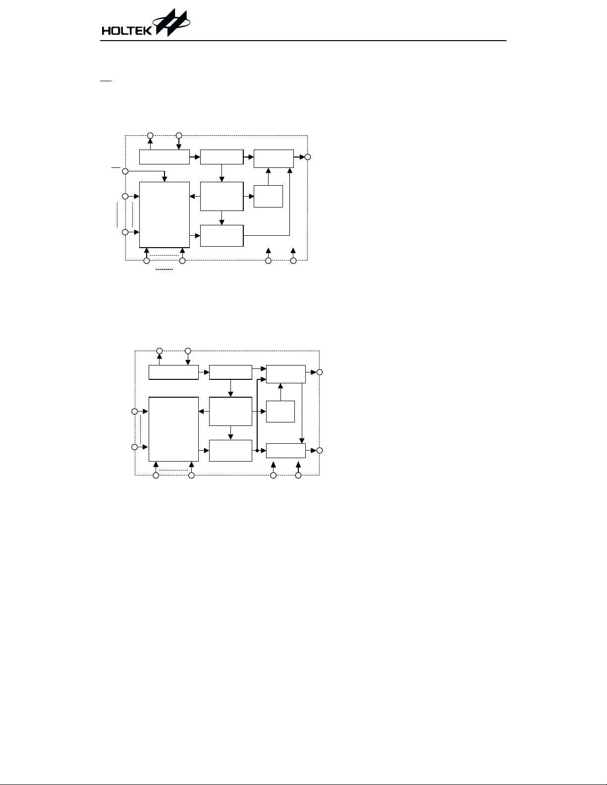
Block Diagram
TE trigger
HT6010
OSC2
312Series of Encoders
OSC1
O s c illa to r
TE
A0
A7
12
Transm ission
G a te C ir c u it
AD8 AD11
DATA trigger
HT6012/HT6014
OSC2
O scillator
Address
Transm ission
G a te C ir c u it
12
OSC1
3 D ivider
¸
12 C ounter
¸
and 1 of 12
D ecoders
Trinary
Detector
3 D iv id e r
¸
12 C ounter
¸
and 1 of 12
D ecoders
Trinary
Detector
D ata S elect
and Buffer
Sync.
Circuit
VDD VSS
D ata S elect
and Buffer
Sync.
Circuit
LED Circuit
DOUT
DOUT
LED
Data
VDD VSS
Note: The address/data pins are available in various combinations (refer to the address/data table).
2 December 13, 1999

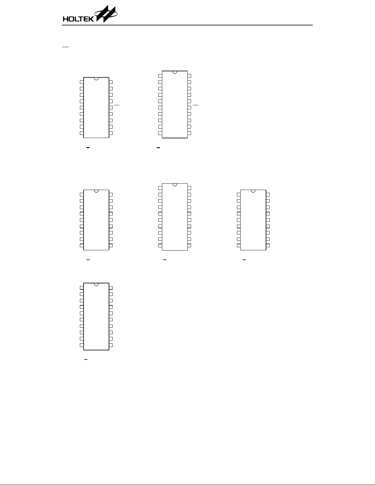
Pin Assignment
T E tr ig g e r ty p e
312Series of Encoders
8-A d dress
4-A ddress/D ata
A0
A1
A2
A3
A4
A5
A6
A7
VSS
18
1
17
2
16
3
15
4
14
5
13
6
12
7
11
8
10
9
H T6010
18 D IP
DATA trigger type
10-A ddress
2 -D a ta
1
A0
A1
A2
A3
A4
A5
A6
A7
VSS
18
2
17
3
16
4
15
5
14
6
13
7
12
8
11
9
10
H T6012
18 D IP
VDD
DOUT
OSC2
OSC1
TE
AD11
AD10
AD9
AD8
VDD
DOUT
OSC2
OSC1
LED
D11
D10
A9
A8
8-A d dress
4-A ddress/D ata
NC
1
A0
2
A1
3
A2
4
A3
5
A4
6
A5
7
A6
8
A7
9
VSS
10
H T 6010
20 D IP/SOP
10-A ddress
2 -D a ta
NC
1
A0
2
A1
3
A2
4
A3
5
A4
6
A5
7
A6
8
A7
9
VSS
10
H T6012
2 0 S O P
NC
20
VDD
19
DOUT
18
OSC2
17
OSC1
16
TE
15
AD11
14
AD10
13
AD9
12
AD8
11
8-A d dress
4 -D a ta
20
NC
19
VDD
18
DOUT
17
OSC2
16
OSC1
15
LED
14
D11
13
D10
12
A9
11
A8
A0
A1
A2
A3
A4
A5
A6
A7
VSS
1
18
2
3
4
5
6
7
8
9
VDD
17
DOUT
16
OSC2
15
OSC1
14
LED
13
D11
12
D10
11
D9
10
D8
H T6014
18 D IP
8-A d dress
4-D ata
NC
1
A0
2
A1
3
A2
4
A3
5
A4
6
A5
7
A6
8
A7
9
VSS
10
H T6014
2 0 S O P
NC
20
VDD
19
DOUT
18
OSC2
17
OSC1
16
LED
15
D11
14
D10
13
D9
12
D8
11
3 December 13, 1999

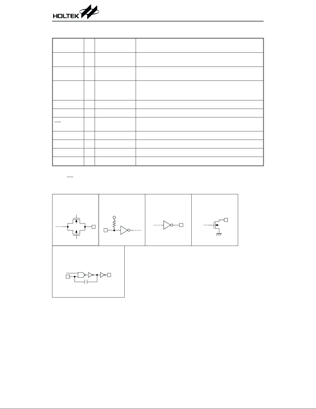
Pin Description
312Series of Encoders
Pin Name I/O
A0~A9 I
AD8~AD11 I
D8~D11 I
Internal
Connection
TRANSMISSION
GATE
TRANSMISSION
GATE
CMOS IN
Pull-high
Description
Input pins for address A0~A9 setting
They can be externally set to VDD or VSS or left open.
Input pins for address/data (AD8~AD11) setting
They can be externally set to VDD or VSS or left open.
Input pins for data (D8~D11) setting and transmission en
able (active low)
They can be externally set to VSS or left open (see Note).
DOUT O CMOS OUT Encoder data serial transmission output
LED O NMOS OUT Transmission enable indicator, active low
TE
I
CMOS IN
Pull-high
Transmission enable, active low (see Note)
OSC1 I OSCILLATOR Oscillator input pin
OSC2 O OSCILLATOR Oscillator output pin
VSS
VDD
¾¾
¾¾
Negative power supply, ground
Positive power supply
Note: D8~D11 are data input and transmission enable pins of the HT6012/HT6014.
TE
is the transmission enable pin of the HT6010.
Approximate internal connections
-
TRANSM ISSIO N
GATE
OSCILLATOR
EN
OSC1
CMOS IN
Pull-high
OSC2
CMOS OUT NMOS OUT
4 December 13, 1999
 Loading...