


HT48RA0A
Preliminary
8-Bit OTP IR Remote Controller
Features
Operating voltage: 2.2V~3.6V
·
Ten bidirectional I/O lines
·
Six schmitt trigger input lines
·
One carrier output (1/2 or 1/3 duty)
·
On-chip crystal and RC oscillator
·
Watchdog timer
·
1K´14 program EPROM
·
32´8 data RAM
·
Low voltage reset function
·
Halt function and wake-up feature reduce
·
power consumption
General Description
The HT48RA0A is an 8-bit high performance
RISC-like microcontroller specifically designed
for multiple I/O product applications. The de
vice is particularly suitable for use in products
62 powerful instructions
·
Up to 1ms instruction cycle with 4MHz
·
system clock
All instructions in 1 or 2 machine cycles
·
14-bit table read instructions
·
One-level subroutine nesting
·
Bit manipulation instructions
·
20-pin SOP package
·
24-pin SOP package
such as infrared remote controllers and various
subsystem controllers. A halt feature is in
cluded to reduce power consumption.
-
-
1 May 17, 2000
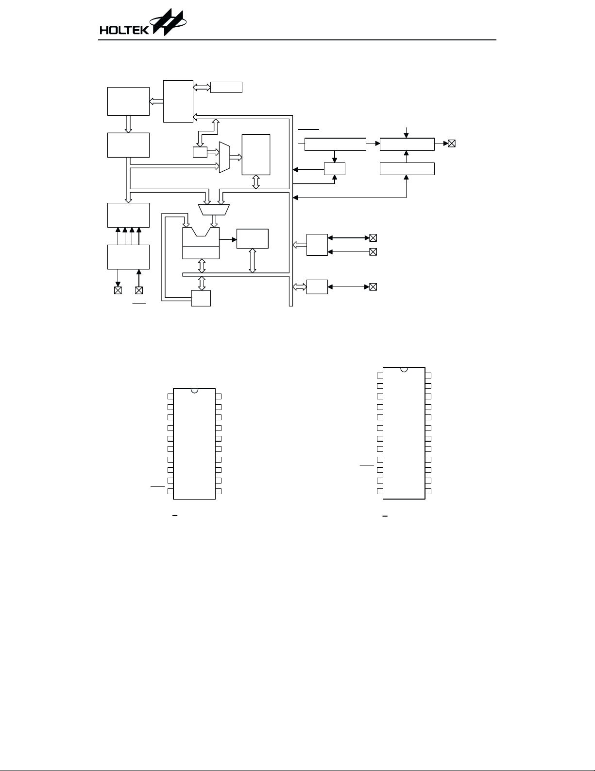
Block Diagram
Preliminary
HT48RA0A
Program
EPRO M
Instruction
R egister
Instruction
D ecoder
G enerator
OSC2
Tim ing
OSC1
RES
VDD
VSS
Program
C ounter
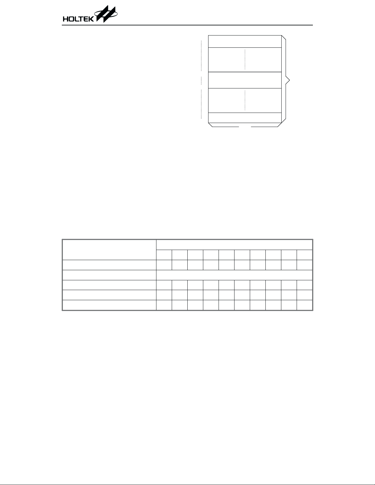
Pin Assignment
MP
ALU
S h ifte r
ACC
STACK
MUX
M
U
X
DATA
Memory
STATUS
SYS CLK/4
Frequency D ivider
WDT
PORT B
PB
PORT A
PA
Level or C arrier
C a r rie r C o n tro l
P C 0 C o n tro l
PB0~PB1
PB2~PB7
PA0~PA7
PC0/REM
PA1
PA0
PB1
PB0
PC0/REM
VDD
OSC2
OSC1
VSS
RES
20
1
19
2
18
3
17
4
16
5
15
6
14
7
13
8
12
9
11
10
H T 4 8 R A 0 A
20 S O P
PA2
PA3
PA4
PA5
PA6
PA7
PB2
PB3
PB4
PB5
PA1
PA0
PB1
PB0
PC0/REM
VDD
OSC2
OSC1
VSS
RES
NC
NC
1
2
3
4
5
6
7
8
9
10
11
12
PA2
24
PA3
23
PA4
22
PA5
21
PA6
20
PA7
19
PB2
18
PB3
17
PB4
16
PB5
15
PB6
14
PB7
13
H T 4 8 R A 0 A
24 S O P
2 May 17, 2000
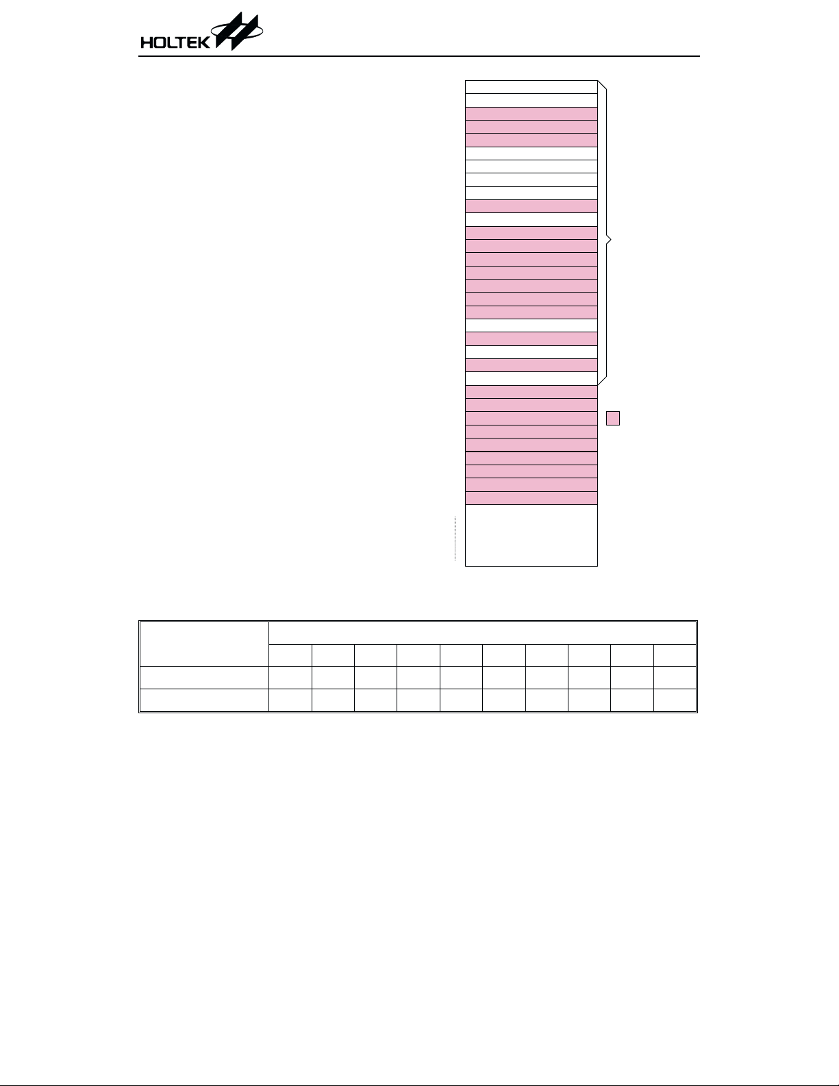
Pin Description
Preliminary
HT48RA0A
Pin Name I/O
PB0, PB1 I/O
PC0/REM O
VDD
OSC2
OSC1
VSS
RES
PB2~PB7 I
PA0~PA7 I/O
¾¾
I
O
¾¾
I
Code
Option
Wake-up
or none
Level or
carrier
Crystal
or RC
¾
Wake-up
or none
¾
Description
2-bit bidirectional input/output lines with pull-high resistors.
Each bit can be determined as NMOS output or schmitt trigger in
put by software instructions. Each bit can also be configured as
wake-up input by code option.
Level or carrier output pin
PC0 can be set as CMOS output pin or carrier output pin by code
option.
Positive power supply
OSC1, OSC2 are connected to an RC network or a crystal (deter
mined by code option) for the internal system clock. In the case of
RC operation, OSC2 is the output terminal for 1/4 system clock
(NMOS open drain output).
Negative power supply, ground
Schmitt trigger reset input. Active low.
6-bit schmitt trigger input lines with pull-high resistors. Each bit
can be configured as a wake-up input by code option.
Bidirectional 8-bit input/output port with pull-high resistors.
Each bit can be determined as NMOS output or schmitt trigger in
put by software instructions.
-
-
-
Absolute Maximum Ratings
Supply Voltage..............................-0.3V to 5.5V
Input Voltage.................V
Note: These are stress ratings only. Stresses exceeding the range specified under ²Absolute Maxi-
mum Ratings² may cause substantial damage to the device. Functional operation of this device
at other conditions beyond those listed in the specification is not implied and prolonged expo
sure to extreme conditions may affect device reliability.
-0.3V to VDD+0.3V
SS
Storage Temperature.................-50°Cto125°C
Operating Temperature ..............-40°Cto85°C
3 May 17, 2000
-
Preliminary
HT48RA0A
D.C. Characteristics
Symbol Parameter
V
I
I
V
V
V
V
I
I
R
R
V
DD
DD
STB
IL1
IH1
IL2
IH2
OL
OH
PH1
PH2
LVR
Operating Voltage
Operating Current 3V
Standby Current 3V
Input Low Voltage for I/O Ports 3V
Input High Voltage for I/O Ports 3V
Input Low Voltage (RES)3V
Input High Voltage (RES)3V
I/O Ports Sink Current 3V
PC0/REM Output Source Current 3V
Pull-high Resistance of PA
Port, PB0~PB1 and RES
Pull-high Resistance of PB2~PB7 3V
Low Voltage Reset 3V
Test Conditions
Conditions
V
DD
LVR disabled 2.2
¾
No load
f
=4MHz
SYS
No load
system HALT
¾
¾
¾
¾
V
=0.1V
OL
V
=0.9V
OH
3V
¾¾60¾ kW
¾¾60¾ kW
¾
Min. Typ. Max. Unit
¾
¾
0.7 1.5 mA
¾¾
DD
DD
0
0.8V
0
0.9V
1.5 2.5
-1 -1.5 ¾
DD
DD
¾
¾
¾
¾
2.1 2.3 2.5 V
3.6 V
1
0.2V
DD
V
DD
0.4V
DD
V
DD
¾
Ta=25°C
mA
V
V
V
V
mA
mA
A.C. Characteristics
Symbol Parameter
f
SYS
t
RES
t
SST
Note: t
System Clock 3V
External Reset Low
Pulse Width
System Start-up timer
Period
=1/f
SYS
SYS
Test Conditions
Min. Typ. Max. Unit
V
DD
¾¾
¾
Conditions
¾
Power-up or
wake-up from HALT
4 May 17, 2000
400
1
¾
¾
¾¾ms
1024
Ta=25°C
4000 kHz
t
¾
SYS
Preliminary
Functional Description
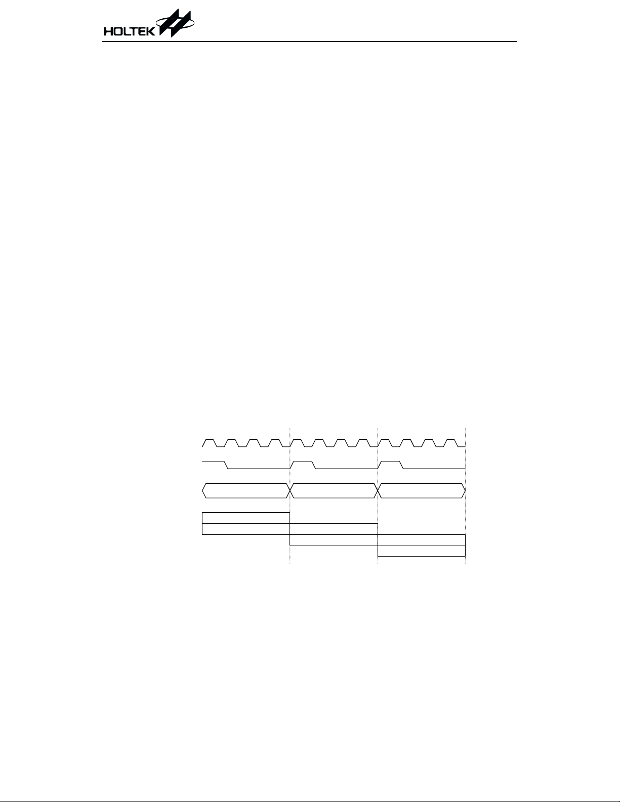
Execution flow
The HT48RA0A system clock can be derived
from a crystal/ceramic resonator oscillator. It is
internally divided into four non-overlapping
clocks. One instruction cycle consists of four
system clock cycles.
Instruction fetching and execution are
pipelined in such a way that a fetch takes one
instruction cycle while decoding and execution
takes the next instruction cycle. However, the
pipelining scheme causes each instruction to ef
fectively execute within one cycle. If an instruc
tion changes the program counter, two cycles
are required to complete the instruction.
Program counter - PC
The 10-bit program counter (PC) controls the
sequence in which the instructions stored in
program EPROM are executed and its contents
specify a maximum of 1024 addresses.
After accessing a program memory word to
fetch an instruction code, the contents of the
program counter are incremented by one. The
program counter then points to the memory
word containing the next instruction code.
When executing a jump instruction, conditional
skip execution, loading PCL register, subroutine call, initial reset or return from subroutine,
the PC manipulates the program transfer by
HT48RA0A
loading the address corresponding to each in
struction.
The conditional skip is activated by instruction.
Once the condition is met, the next instruction,
fetched during the current instruction execu
tion, is discarded and a dummy cycle replaces it
to get the proper instruction. Otherwise pro
ceed with the next instruction.
The lower byte of the program counter (PCL) is
a readable and writeable register (06H).
Moving data into the PCL performs a short
jump. The destination will be within 256 loca
tions.
When a control transfer takes place, an addi
tional dummy cycle is required.
Program memory - EPROM
The program memory is used to store the pro
gram instructions which are to be executed. It
also contains data and table and is organized
into 1024´14 bits, addressed by the program
counter and table pointer.
Certain locations in the program memory are
reserved for special usage:
·
Location 000H
This area is reserved for the initialization
program. After chip reset, the program always begins execution at location 000H.
-
-
-
-
-
-
S ystem C lock
Instruction C ycle
PC
T1 T2 T3 T4 T1 T2 T3 T4 T1 T2 T3 T4
PC PC+1 PC+2
F e tc h IN S T (P C )
Execute IN S T (PC -1)
F e tc h IN S T (P C + 1 )
Execute IN S T (PC )
F e tc h IN S T (P C + 2 )
Execute IN S T (PC +1)
Execution flow
5 May 17, 2000
Preliminary
HT48RA0A
·
Table location
Any location in the EPROM space can be used
as look-up tables. The instructions TABRDC
[m] (the current page, 1 page=256 words) and
TABRDL [m] (the last page) transfer the con
tents of the lower-order byte to the specified
data memory, and the higher-order byte to
TBLH (08H). Only the destination of the
lower-order byte in the table is well-defined,
the other bits of the table word are trans
ferred to the lower portion of TBLH, the re
maining 2 bits are read as ²0². The Table
Higher-order byte register (TBLH) is read
only. The table pointer (TBLP) is a read/write
register (07H), where P indicates the table lo
cation. Before accessing the table, the loca
tion must be placed in TBLP. The TBLH is
read only and cannot be restored. All table re
lated instructions need 2 cycles to complete
the operation. These areas may function as
normal program memory depending upon the
requirements.
Stack register - STACK
This is a special part of the memory used to
save the contents of the program counter (PC)
only. The stack is organized into one level and is
neither part of the data nor part of the program
space, and is neither readable nor writeable.
The activated level is indexed by the stack
000H
D evice initialization program
-
n00H
nFFH
Look-up table (256 w ords)
-
-
3FFH
-
-
pointer (SP) and is neither readable nor
Look-up table (256 w ords)
14 bits
N ote: n ranges from 0 to 3
Program memory
writeable. At a subroutine call the contents of
the program counter are pushed onto the stack.
At the end of a subroutine signaled by a return
instruction (RET), the program counter is re
stored to its previous value from the stack. Af
ter a chip reset, the SP will point to the top of the
stack.
If the stack is full and a ²CALL² is subsequently
executed, stack overflow occurs and the first entry will be lost (only the most recent return address is stored).
Program
ERO M
-
-
Mode
Program Counter
*9 *8 *7 *6 *5 *4 *3 *2 *1 *0
Initial reset 0000000000
Skip PC+2
Loading PCL *9 *8 @7 @6 @5 @4 @3 @2 @1 @0
Jump, call branch #9 #8 #7 #6 #5 #4 #3 #2 #1 #0
Return from subroutine S9 S8 S7 S6 S5 S4 S3 S2 S1 S0
Program counter
Note: *9~*0: Program counter bits S9~S0: Stack register bits
#9~#0: Instruction code bits @7~@0: PCL bits
6 May 17, 2000
Preliminary
HT48RA0A
Data memory - RAM
The data memory is designed with 42´8 bits.
The data memory is divided into two functional
groups: special function registers and general
purpose data memory (32´8). Most of them are
read/write, but some are read only.
The special function registers include the indirect
addressing register (00H), the memory pointer
register (MP;01H), the accumulator (ACC;05H)
the program counter lower-order byte register
(PCL;06H), the table pointer (TBLP;07H), the ta
ble higher-order byte register (TBLH;08H), the
status register (STATUS;0AH) and the I/O regis
ters (PA;12H, PB;14H, PC;16H). The remaining
space before the 20H is reserved for future ex
panded usage and reading these locations will re
turn the result 00H. The general purpose data
memory, addressed from 20H to 3FH, is used for
data and control information under instruction
command.
All data memory areas can handle arithmetic,
logic, increment, decrement and rotate opera
tions directly. Except for some dedicated bits,
each bit in the data memory can be set and re
set by the SET [m].i and CLR [m].i instructions,
respectively. They are also indirectly accessible
through memory pointer register (MP;01H).
Indirect addressing register
Location 00H is an indirect addressing register
that is not physically implemented. Any
read/write operation of [00H] accesses data
memory pointed to by MP (01H). Reading location 00H itself indirectly will return the result
-
-
-
-
-
-
Indirect Addressing R egister
00H
01H
02H
03H
04H
05H
06H
07H
08H
09H
0AH
0BH
0C H
0D H
0EH
0FH
10H
11H
12H
13H
14H
15H
16H
17H
18H
19H
1AH
1BH
1C H
1D H
1EH
1FH
20H
G eneral P urpose
DATA M EMO RY
3FH
MP
ACC
PCL
TBLP
TBLH
STATUS
Special P urpose
DATA M EMO RY
PA
PB
PC
: U n u s e d
R ead as "00"
(32 Bytes)
RAM mapping
00H. Writing indirectly results in no operation.
Table Location
Instruction(s)
*9 *8 *7 *6 *5 *4 *3 *2 *1 *0
TABRDC [m] P9 P8 @7 @6 @5 @4 @3 @2 @1 @0
TABRDL [m] 1 1 @7 @6 @5 @4 @3 @2 @1 @0
Table location
Note: *9~*0: Table location bits @7~@0: Table pointer bits
P9~P8: Current program counter bits
7 May 17, 2000

Preliminary
HT48RA0A
The memory pointer register MP (01H) is a
6-bit register. The bit 7~6 of MP is undefined
and reading will return the result ²1². Any writ
ing operation to MP will only transfer the lower
6-bit data to MP.
Accumulator
The accumulator closely relates to ALU opera
tions. It is also mapped to location 05H of the
data memory and is capable of carrying out im
mediate data operations. Data movement be
tween two data memory locations has to pass
through the accumulator.
Arithmetic and logic unit - ALU
This circuit performs 8-bit arithmetic and logic
operation. The ALU provides the following
functions.
·
Arithmetic operations (ADD, ADC, SUB,
SBC, DAA)
·
Logic operations (AND, OR, XOR, CPL)
·
Rotation (RL, RR, RLC, RRC)
·
Increment and Decrement (INC, DEC)
Labels Bits Function
C is set if the operation results in a carry during an addition operation or if a bor-
C0
AC 1
Z2
OV 3
PD 4
TO 5
¾
¾
row does not take place during a subtraction operation; otherwise C is cleared. C
is also affected by a rotate through carry instruction.
AC is set if the operation results in a carry out of the low nibbles in addition or no
borrow from the high nibble into the low nibble in subtraction; otherwise AC is
cleared.
Z is set if the result of an arithmetic or logic operation is zero; otherwise Z is
cleared.
OV is set if the operation results in a carry into the highest-order bit but not a
carry out of the highest-order bit, or vice versa; otherwise OV is cleared.
PD is cleared when either a system power-up or executing the CLR WDT in
struction. PD is set by executing the HALT instruction.
TO is cleared by a system power-up or executing the CLR WDT or HALT instruc
tion. TO is set by a WDT time-out.
6
Undefined, read as ²0²
7
Undefined, read as ²0²
·
Branch decision (SZ, SNZ, SIZ, SDZ ....)
The ALU not only saves the results of a data op
eration but also changes the contents of the sta
tus register.
Status register - STATUS
This 8-bit status register (0AH) contains the zero
flag (Z), carry flag (C), auxiliary carry flag (AC),
overflow flag (OV), power down flag (PD) and
watchdog time-out flag (TO). It also records the
status information and controls the operation se
quence.
With the exception of the TO and PD flags, bits
in the status register can be altered by instruc
tions like most other register. Any data written
into the status register will not change the TO
or PD flags. In addition it should be noted that
operations related to the status register may
give different results from those intended. The
TO and PD flags can only be changed by the
Watchdog Timer overflow, chip power-up, clear
ing the Watchdog Timer and executing the
HALT instruction.
-
-
-
-
-
-
-
Status register
8 May 17, 2000
Preliminary
HT48RA0A
The Z, OV, AC and C flags generally reflect the
status of the latest operations.
In addition, on executing the subroutine call,
the status register will not be automatically
pushed onto the stack. If the contents of the sta
tus are important and if the subroutine can cor
rupt the status register, precautions must be
taken to save it properly.
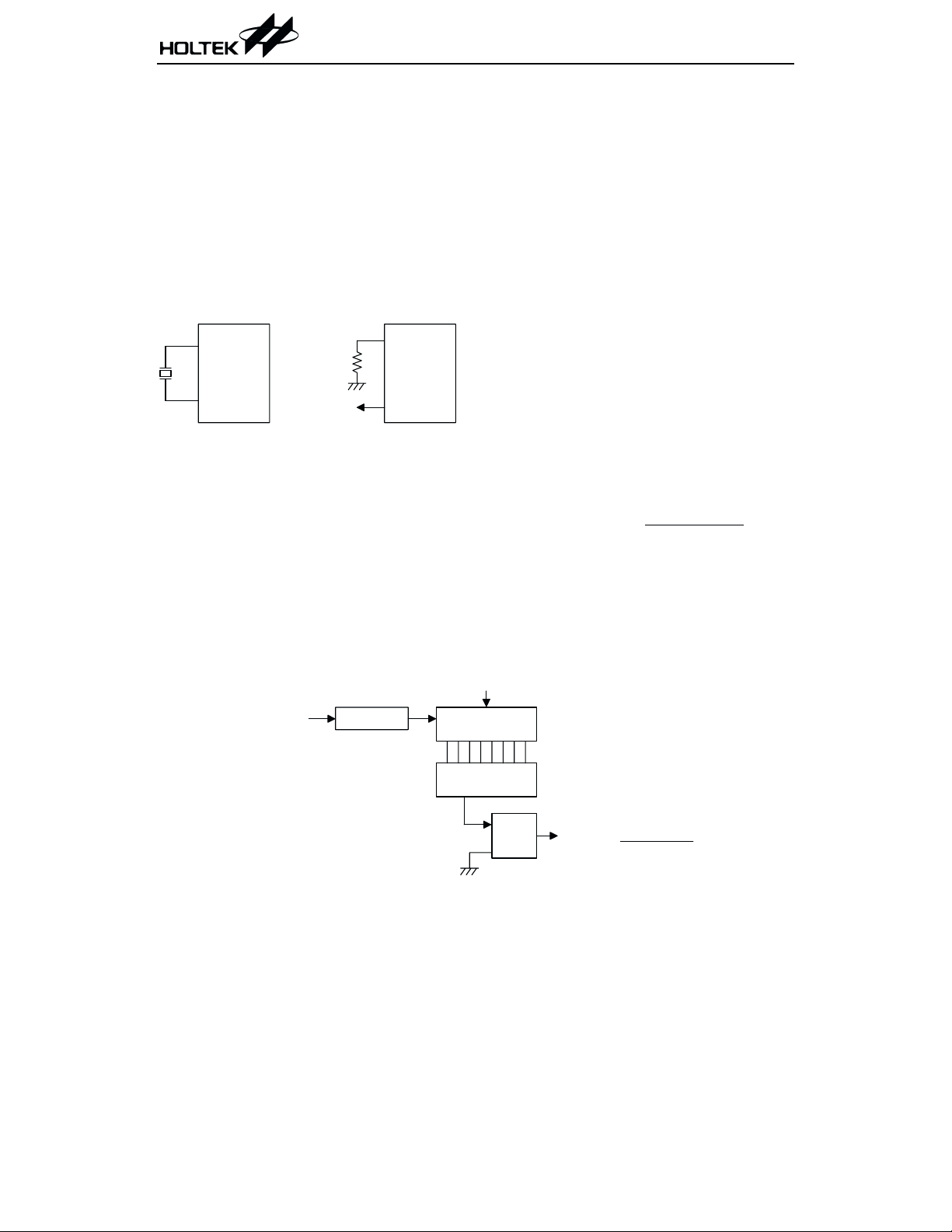
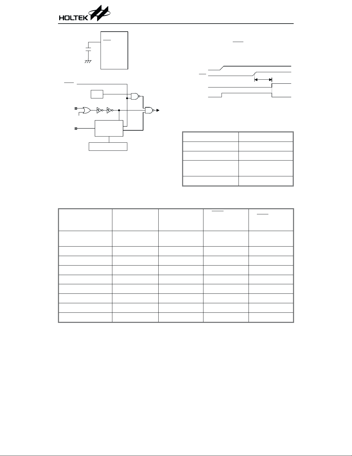
Oscillator configuration
There are two oscillator circuits in the
HT48RA0A.
/4
OSC1
OSC2
R C O scillator
OSC1
OSC2
C rystal O scilla tor
f
SYS
(N M O S open
drain output)
System oscillator
Both are designed for system clocks; the RC os
cillator and the Crystal oscillator, which are de
termined by code options. No matter what
oscillator type is selected, the signal provides
the system clock. The HALT mode stops the
system oscillator and ignores the external signal to conserve power.
If an RC oscillator is used, an external resistor
between OSC1 and VSS in needed and the resistance must range from 51kW to 1MW. The
system clock, divided by 4, is available on
OSC2, which can be used to synchronize exter
nal logic. The RC oscillator provides the most
cost effective solution. However, the frequency
of the oscillation may vary with V
ture and the chip itself due to process varia
tions. It is, therefore, not suitable for timing
sensitive operations where accurate oscillator
frequency is desired.
If the Crystal oscillator is used, a crystal across
OSC1 and OSC2 is needed to provide the feed
back and phase shift for the oscillator. No other
external components are needed. Instead of a
crystal, the resonator can also be connected be
tween OSC1 and OSC2 to get a frequency refer
ence, but two external capacitors in OSC1 and
OSC2 are required.
Watchdog timer - WDT
The clock source of the WDT is implemented by
instruction clock (system clock divided by 4).
The clock source is processed by a frequency di
vider and a prescaller to yield various time out
periods.
-
WDT time out period =
Clock Source
n
2
Where n= 8~11 selected by code option.
This timer is designed to prevent a software
malfunction or sequence jumping to an unknown location with unpredictable results. The
Watchdog Timer can be disabled by code option.
If the Watchdog Timer is disabled, all the exe-
, tempera
DD
-
-
-
-
-
-
-
C lo ck S o urce
(S ystem C lock/4 )
Frequency D ivider
3-bit Counter
Clear W DT
P resca lle r
(8 -b it)
Code Option
Select
C ode
Option
Watchdog timer
9 May 17, 2000
WDT
Tim e-out
C lo ck S o urce
n
2
(n=8~11)
Preliminary
HT48RA0A
cutions related to the WDT result in no opera
tion and the WDT will lose its protection
purpose. In this situation the logic can only be
restarted by an external logic.
A WDT overflow under normal operation will ini
tialize ²chip reset² and set the status bit ²TO².To
clear the contents of the WDT prescaler, three
methods are adopted; external reset (a low level
to RES
), software instructions, or a HALT in
struction. There are two types of software in
structions. One type is the single instruction
²CLR WDT², the other type comprises two in
structions, ²CLR WDT1² and ²CLR WDT2².Of
these two types of instructions, only one can be
active depending on the code option -²CLR WDT
times selection option².Ifthe²CLR WDT² is se
lected (i.e.. CLRWDT times equal one), any execu
tion of the CLR WDT instruction will clear the
WDT. In case ²CLR WDT1² and ²CLR WDT2² are
chosen (i.e.. CLRWDT times equal two), these two
instructions must be executed to clear the WDT;
otherwise, the WDT may reset the chip due to a
time-out.
Power down operation - HALT
The HALT mode is initialized by the HALT instruction and results in the following...
·
The system oscillator turns off and the WDT
stops.
·
The contents of the on-chip RAM and registers remain unchanged.
·
WDT prescaler are cleared.
·
All I/O ports maintain their original status.
·
The PD flag is set and the TO flag is cleared.
The system can quit the HALT mode by means
of an external reset or an external falling edge
signal on port B. An external reset causes a de
vice initialization. Examining the TO and PD
flags, the reason for chip reset can be deter
mined. The PD flag is cleared when the system
powers up or execute the CLR WDT instruction
and is set when the HALT instruction is exe
cuted. The TO flag is set if the WDT time-out oc
curs, and causes a wake-up that only resets the
PC (Program Counter) and SP, the others keep
their original status.
The port B wake-up can be considered as a con
tinuation of normal execution. Each bit in port
B can be independently selected to wake up the
device by the code option. Awakening from an
I/O port stimulus, the program will resume exe
cution of the next instruction.
-
Once a wake-up event(s) occurs, it takes 1024
t
(system clock period) to resume normal op
SYS
eration. In other words, a dummy cycle period
will be inserted after the wake-up.
To minimize power consumption, all I/O pins
should be carefully managed before entering
the HALT status.
Reset
There are three waysin which a reset canoccur:
·
RES reset during normal operation
·
RES reset during HALT
·
WDT time-out reset during normal
operation
Some registers remain unchanged during reset
conditions. Most registers are reset to the ²initial condition² when the reset conditions are
met. By examining the PD and TO flags, the
program can distinguish between different
²chip resets².
TO PD RESET Conditions
0 0 RES
uu
-
-
-
0 1 RES
1u
Note: ²u² means ²unchanged².
reset during power-up
reset during normal
RES
operation
wake-up HALT
WDT time-out during normal
operation
-
-
-
-
10 May 17, 2000
Preliminary
t
HT48RA0A
When a system power up occurs, an SST delay
RES
is added during the reset period. But when the
reset comes from the RES
pin, the SST delay is
disabled. Any wake-up from HALT will enable
the SST delay.
VDD
HALT
RES
OSC1
LVR R eset
Reset circuit
WDT
WDT
Tim e-out
Reset
SST
10-stage
R ipple C ounter
Rese
RES
SST Tim e-out
C hip R eset
t
SST
Reset timing chart
The functional unit chip reset status is shown be
low.
PC 000H
Power-on Detection
Reset configuration
To guarantee that the system oscillator has
started and stabilized, the SST (System
Start-up Timer) provides an extra-delay of 1024
WDT Prescaler Clear
Input/output ports Input mode
SP
Points to the top of the
stack
Carrier Output Low level
system clock pulses when the system powers up
or when the system awakes from a HALT state.
The chip reset status of the registers is summarized in the following table:
Reset
RES
(Normal
Operation)
RES
(HALT)
Register
PC
(Program Counter)
Reset
(Power On)
WDT Time-out
(Normal
Operation)
000H 000H 000H 000H
MP -xxx xxxx -uuu uuuu -uuu uuuu -uuu uuuu
ACC xxxx xxxx uuuu uuuu uuuu uuuu uuuu uuuu
TBLP xxxx xxxx uuuu uuuu uuuu uuuu uuuu uuuu
TBLH --xx xxxx --uu uuuu --uu uuuu --uu uuuu
STATUS --00 xxxx --1u uuuu --uu uuuu --01 uuuu
PA 1111 1111 1111 1111 1111 1111 1111 1111
PB 1111 1111 1111 1111 1111 1111 1111 1111
PC ---- ---1 ---- ---1 ---- ---1 ---- ---1
-
Reset
Note:
²u² means ²unchanged²
²x² means ²unknown²
11 May 17, 2000
Preliminary
HT48RA0A
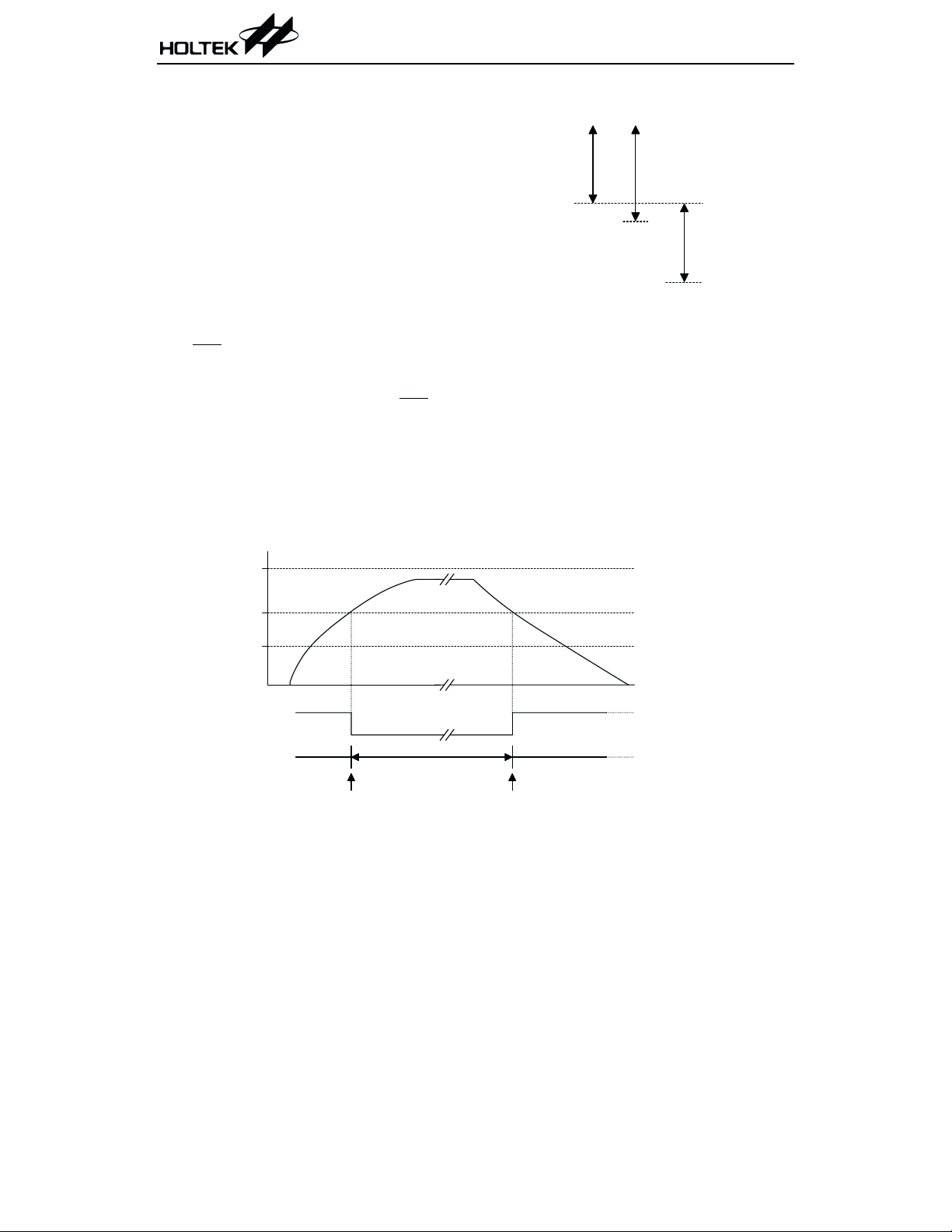
Low voltage reset - LVR
The HT48RA0A provides low voltage reset cir
cuit in order to monitor the supply voltage of
the device. If the supply voltage of the device is
within the range 0.9V~2.3V, such as changing a
battery, the LVR will automatically reset the
device internally.
The LVR includes the following specifications:
·
The low voltage (0.9V~2.3V) has to remain in
their original state to exceed 1 ms. If the low
voltage state does not exceed 1 ms, the LVR
will ignore it and do not perform a reset func
tion.
·
The LVR uses the ²OR² function with the exter
nal RES
·
During HALT mode, if the LVR occurs, the
signal to perform chip reset.
device will wake-up and the PD flag will be
DD
.
)is
set as ²1², the same as the external RES
Because the operating voltage (V
2.3V~3.6V and the LVR operating voltage
(V
) is 0.9V~2.3V, therefore one margin volt
LVR
age about 0.1V is needed for proper chip opera
tion. The relationship between V
DD
and V
LVR
shown below.
V
DD
3.6V
V
DDVOPR
3.6V
2.3V
3.6V
2.2V
V
LVR
0.9V
-
-
Note: V
-
is the voltage range for proper chip
OPR
operation at 4MHz system clock.
Carrier
The HT48RA0A provides a carrier output
which shares the pin with PC0. It can be se
lected to be a carrier output (REM) or level out
put pin (PC0) by code option. If the carrier
output option is selected, setting PC0=²0² to en
-
able carrier output and setting PC0=²1² to dis
able it at low level output.
is
-
-
-
-
V
LVR
0.9V
0V
R eset S ignal
Reset
N orm al O peration R eset
*1 *2
LVR D etect Voltage
V
= 0.9~2.3V
LVR
Low voltage reset
Note: *1: To make sure that the system oscillator has stabilized, the SST provides an extra delay of
1024 system clock pulses before entering the normal operation.
*2: Since the low voltage has to maintain in its original state and exceed 1ms, therefore 1ms
delay enter the reset mode.
12 May 17, 2000

Preliminary
HT48RA0A
The clock source of the carrier is implemented
by instruction clock (system clock divided by 4)
and processed by a frequency divider to yield
various carry frequency.
Carry Frequency=
Clock Source
n
´
m2
where m=2 or 3 and n=0~3, both are selected by
code option. If m=2, the duty cycle of the carrier
output is 1/2 duty. If m=3, the duty cycle of the
carrier output can be 1/2 duty or 1/3 duty also
determined by code option (with the exception
of n=0).
Detailed selection of the carrier duty is shown
below:
m´2
n
Duty Cycle
2, 4, 8, 16 1/2
3 1/3
6, 12, 24 1/2 or 1/3
The following table shows examples of carrier
frequency selection.
f
SYS
455kHz
f
CARRIER
37.92kHz
56.9kHz
Duty
1
only
3
1
only
2
m´2
3
2
n
Input/output ports
There are an 8-bit bidirectional input/output
port, a 6-bit input with 2-bit I/O port and
one-bit output port in the HT48RA0A, labeled
PA, PB and PC which are mapped to [12H],
[14H], [16H] of the RAM, respectively. Each bit
of PA can be selected as NMOS output or
schmitt trigger with pull-high resistor by soft
ware instruction. PB0~PB1 have the same
structure with PA, while PB2~PB7 can only be
used for input operation (schmitt trigger with
pull-high resistors). PC is only one-bit output
port shares the pin with carrier output. If the
level option is selected, the PC is CMOS output.
Both PA and PB for the input operation, these
ports are non-latched, that is, the inputs should
be ready at the T2 rising edge of the instruction
²MOV A, [m]² (m=12H or 14H). For PA,
PB0~PB1 and PC output operation, all data are
latched and remain unchanged until the output
latch is rewritten.
When the PA and PB0~PB1 is used for input op
eration, it should be noted that before reading
data from pads, a ²1² should be written to the
related bits to disable the NMOS device. That
is, the instruction ²SET [m].i² (i=0~7 for PA,
i=0~1 for PB) is executed first to disable related
NMOS device, and then ²MOV A, [m]² to get
stable data.
-
-
C lo ck S o urce
(S ystem C lock/4)
Frequency D ivider
3-bit C ounter
Code Option
1/2 or 1/3 duty
1/2
1/3
R ead path for read-m odify-w rite
Carrier Duty
Select
Carrier/Level output
13 May 17, 2000
V
DD
Level
Carrier
P C 0 D a ta R e g is te r
C ode O ption
(c a rrie r o r le ve l)
Carrier
Level
REM/PC0

Preliminary
HT48RA0A
After chip reset, PA and PB remain at a high
level input line while PC remain at high level
output, if the level option is selected.
Each bit of PA, PB0~PB1 and PC output latches
can be set or cleared by the ²SET [m].i² and
²CLR [m].i² (m=12H, 14H or 16H) instructions
respectively.
Some instructions first input data and then fol
low the output operations. For example, ²SET
R ead D ata
D ata bus
System W ake-up
C ode O ption
PB input lines
D ata bus
Write
C hip R eset
D
CK
S
[m].i², ²CLR [m]², ²CPL [m]², ²CPLA [m]² read
the entire port states into the CPU, execute the
defined operations (bit-operation), and then
write the results back to the latches or to the ac
cumulator.
Each line of PB has a wake-up capability to the
device by code option. The highest seven bits of
PC are not physically implemented, on reading
them a ²0² is returned and writing results in a
no-operation.
V
DD
Pull-up
PB2~PB7
V
DD
W eak
Q
Q
Pull-up
PA0~PA7
PB0~PB1
-
R ead D ata
System W ake-up
C ode O ption
PB0~PB1 only
PA, PB Input/output lines
14 May 17, 2000

Preliminary
Code option
The following table shows eight kinds of code option in the HT48RA0A. All the code options must be
defined to ensure proper system functioning.
No. Code Option
WDT time-out period selection
1
Time-out period=
WDT enable/disable selection. This option is to decide whether the WDT timer is enabled
2
or disabled.
CLRWDT times selection. This option defines how to clear the WDT by instruction. ²One
time² means that the CLR WDT instruction can clear the WDT. ²Two times² means only
3
if both of the CLR WDT1 and CLR WDT2 instructions have been executed, the WDT can
be cleared.
Wake-up selection. This option defines the wake-up activity function. External input pins
4
(PB only) all have the capability to wake-up the chip from a HALT.
Carrier/level output selection. This option defines the activity of PC0 to be carrier output
5
or level output.
Carry frequency selection.
6
Carry frequency=
Clock Source
n
2
Clock Source
(2 or 3) 2
´
where n=8~11.
where n=0~3.
n
HT48RA0A
Carrier duty selection. There are two types of selection: 1/2 duty or 1/3 duty.
If carrier frequency= Clock Source /(2, 4, 8 or 16), the duty cycle will be 1/2 duty.
7
If carrier frequency= Clock Source /3, the duty cycle will be 1/3 duty.
If carrier frequency= Clock Source /(6, 12 or 24), the duty cycle can be 1/2 duty or 1/3 duty.
OSC type selection. This option is to decide if an RC or Crystal oscillator is chosen as sys-
8
tem clock. If the Crystal oscillator is selected, the XST (Crystal Start-up Timer) default is
activated, otherwise the XST is disabled.
15 May 17, 2000

Application Circuits
Preliminary
HT48RA0A
PB1
V
DD
100mF
1
W
120W~240
300pF
X'tal
(see N ote)
300pF
100k
W
0.1mF
Note:
It is recommended that a 100mF decoupling capacitor is placed between VSS and VDD.
PB0
PA3
PA2
PA1
PA0
W
HT48RA0A
PC0/REM
OSC1
OSC2
RES
PB2
PB3
PB4
PB5
PB6
PB7
PA7
PA6
PA5
PA4
If the crystal has a value above 1MHz the capacitors are not required.
The resistance and capacitance for reset circuit should be designed to ensure that the VDD is
stable and remains in a valid range of the operating voltage before bringing RES
to high.
16 May 17, 2000

Instruction Set Summary
Preliminary
HT48RA0A
Mnemonic Description
Arithmetic
ADD A,[m]
ADDM A,[m]
ADD A,x
ADC A,[m]
ADCM A,[m]
SUB A,x
SUB A,[m]
SUBM A,[m]
Add data memory to ACC
Add ACC to data memory
Add immediate data to ACC
Add data memory to ACC with carry
Add ACC to register with carry
Subtract immediate data from ACC
Subtract data memory from ACC
Subtract data memory from ACC with result in
data memory
SBC A,[m]
SBCM A,[m]
Subtract data memory from ACC with carry
Subtract data memory from ACC with carry with
result in data memory
DAA [m]
Decimal adjust ACC for addition with result in
data memory
Logic Operation
AND A,[m]
OR A,[m]
XOR A,[m]
ANDM A,[m]
ORM A,[m]
XORM A,[m]
AND A,x
OR A,x
XOR A,x
CPL [m]
CPLA [m]
AND data memory to ACC
OR data memory to ACC
Exclusive-OR data memory to ACC
AND ACC to data memory
OR ACC to data memory
Exclusive-OR ACC to data memory
AND immediate data to ACC
OR immediate data to ACC
Exclusive-OR immediate data to ACC
Complement data memory
Complement data memory with result in ACC
Increment & Decrement
INCA [m]
INC [m]
DECA [m]
DEC [m]
Increment data memory with result in ACC
Increment data memory
Decrement data memory with result in ACC
Decrement data memory
Instruction
Cycle
1
(1)
1
1
1
(1)
1
1
1
(1)
1
1
(1)
1
(1)
1
1
1
1
(1)
1
(1)
1
(1)
1
1
1
1
(1)
1
1
1
(1)
1
1
(1)
1
Flag Affected
Z,C,AC,OV
Z,C,AC,OV
Z,C,AC,OV
Z,C,AC,OV
Z,C,AC,OV
Z,C,AC,OV
Z,C,AC,OV
Z,C,AC,OV
Z,C,AC,OV
Z,C,AC,OV
C
Z
Z
Z
Z
Z
Z
Z
Z
Z
Z
Z
Z
Z
Z
Z
17 May 17, 2000

Preliminary
HT48RA0A
Mnemonic Description
Rotate
RRA [m]
RR [m]
RRCA [m]
Rotate data memory right with result in ACC
Rotate data memory right
Rotate data memory right through carry with re
sult in ACC
RRC [m]
RLA [m]
RL [m]
RLCA [m]
Rotate data memory right through carry
Rotate data memory left with result in ACC
Rotate data memory left
Rotate data memory left through carry with result
in ACC
RLC [m]
Rotate data memory left through carry
Data Move
MOV A,[m]
MOV [m],A
MOV A,x
Move data memory to ACC
Move ACC to data memory
Move immediate data to ACC
Bit Operation
CLR [m].i
SET [m].i
Clear bit of data memory
Set bit of data memory
Branch
JMP addr
SZ [m]
SZA [m]
Jump unconditionally
Skip if data memory is zero
Skip if data memory is zero with data movement
to ACC
SZ [m].i
SNZ [m].i
SIZ [m]
SDZ [m]
SIZA [m]
Skip if bit i of data memory is zero
Skip if bit i of data memory is not zero
Skip if increment data memory is zero
Skip if decrement data memory is zero
Skip if increment data memory is zero with result
in ACC
SDZA [m]
Skip if decrement data memory is zero with result
in ACC
CALL addr
RET
RET A,x
Subroutine call
Return from subroutine
Return from subroutine and load immediate data
to ACC
Table Read
TABRDC [m]
Read EPROM code (current page) to data memory
and TBLH
TABRDL [m]
Read EPROM code (last page) to data memory and
TBLH
Instruction
Cycle
1
(1)
1
-
1
(1)
1
1
(1)
1
1
(1)
1
1
(1)
1
1
(1)
1
(1)
1
2
(2)
1
(2)
1
(2)
1
(2)
1
(3)
1
(3)
1
(2)
1
(2)
1
2
2
2
(1)
2
(1)
2
Flag Affected
None
None
C
C
None
None
C
C
None
None
None
None
None
None
None
None
None
None
None
None
None
None
None
None
None
None
None
18 May 17, 2000

Preliminary
HT48RA0A
Mnemonic Description
Miscellaneous
NOP
CLR [m]
SET [m]
CLR WDT
CLR WDT1
CLR WDT2
SWAP [m]
SWAPA [m]
HALT
No operation
Clear data memory
Set data memory
Clear Watchdog timer
Pre-clear Watchdog timer
Pre-clear Watchdog timer
Swap nibbles of data memory
Swap nibbles of data memory with result in ACC
Enter power down mode
Note: x: 8 bits immediate data
m: 7 bits data memory address
A: accumulator
i: 0~7 number of bits
addr: 11 bits program memory address
Ö: Flag(s) is affected
-: Flag(s) is not affected
(1)
: If a loading to the PCL register occurs, the execution cycle of instructions will be
delayed for one more cycle (4 system clocks).
(2)
: If a skip to the next instruction occurs, the execution cycle of instructions will be
delayed for one more cycle (4 system clocks). Otherwise the original instruction
cycle(s) is unchanged.
(3):(1)
(4)
: The flags may be affected by the execution status. If the watchdog timer is cleared
and
(2)
by executing the CLR WDT1 or CLR WDT2 instruction, the TO is set and the PD is
cleared. Otherwise the TO and PD flags remain unchanged.
Instruction
Cycle
1
(1)
1
(1)
1
1
1
1
(1)
1
1
1
Flag Affected
None
None
None
TO,PD
(4)
(4)
,PD
,PD
(4)
(4)
TO
TO
None
None
TO,PD
19 May 17, 2000

Preliminary
HT48RA0A
Instruction Definition
ADC A,[m] Add data memory and carry to the accumulator
Description The contents of the specified data memory, accumulator and the carry flag
are added simultaneously, leaving the result in the accumulator.
Operation
Affected flag(s)
ADCM A,[m] Add the accumulator and carry to data memory
Description The contents of the specified data memory, accumulator and the carry flag
Operation
Affected flag(s)
ADD A,[m] Add data memory to the accumulator
Description The contents of the specified data memory and the accumulator are added.
Operation
Affected flag(s)
ACC ¬ ACC+[m]+C
TC2 TC1 TO PD OV Z AC C
¾¾¾¾ÖÖÖÖ
are added simultaneously, leaving the result in the specified data memory.
[m] ¬ ACC+[m]+C
TC2 TC1 TO PD OV Z AC C
¾¾¾¾ÖÖÖÖ
The result is stored in the accumulator.
ACC ¬ ACC+[m]
TC2 TC1 TO PD OV Z AC C
¾¾¾¾ÖÖÖÖ
ADD A,x Add immediate data to the accumulator
Description The contents of the accumulator and the specified data are added, leaving
the result in the accumulator.
Operation
Affected flag(s)
ACC ¬ ACC+x
TC2 TC1 TO PD OV Z AC C
¾¾¾¾ÖÖÖÖ
20 May 17, 2000

Preliminary
ADDM A,[m] Add the accumulator to the data memory
Description The contents of the specified data memory and the accumulator are added.
The result is stored in the data memory.
Operation
Affected flag(s)
AND A,[m] Logical AND accumulator with data memory
Description Data in the accumulator and the specified data memory perform a bitwise
Operation
Affected flag(s)
AND A,x Logical AND immediate data to the accumulator
Description Data in the accumulator and the specified data perform a bitwise logi
Operation
Affected flag(s)
[m] ¬ ACC+[m]
TC2 TC1 TO PD OV Z AC C
¾¾¾¾ÖÖÖÖ
logical_AND operation. The result is stored in the accumulator.
ACC ¬ ACC ²AND² [m]
TC2 TC1 TO PD OV Z AC C
¾¾¾¾¾Ö¾¾
cal_AND operation. The result is stored in the accumulator.
ACC ¬ ACC ²AND² x
TC2 TC1 TO PD OV Z AC C
¾¾¾¾¾Ö¾¾
HT48RA0A
-
ANDM A,[m] Logical AND data memory with the accumulator
Description Data in the specified data memory and the accumulator perform a bitwise
logical_AND operation. The result is stored in the data memory.
Operation
Affected flag(s)
[m] ¬ ACC ²AND² [m]
TC2 TC1 TO PD OV Z AC C
¾¾¾¾¾Ö¾¾
21 May 17, 2000

Preliminary
CALL addr Subroutine call
Description The instruction unconditionally calls a subroutine located at the indicated
address. The program counter increments once to obtain the address of the
next instruction, and pushes this onto the stack. The indicated address is
then loaded. Program execution continues with the instruction at this ad
dress.
Operation
Affected flag(s)
CLR [m] Clear data memory
Description The contents of the specified data memory are cleared to zero.
Operation
Affected flag(s)
CLR [m].i Clear bit of data memory
Description The bit i of the specified data memory is cleared to zero.
Operation
Affected flag(s)
Stack ¬ PC+1
PC ¬ addr
TC2 TC1 TO PD OV Z AC C
¾¾¾¾¾¾¾¾
[m] ¬ 00H
TC2 TC1 TO PD OV Z AC C
¾¾¾¾¾¾¾¾
[m].i ¬ 0
TC2 TC1 TO PD OV Z AC C
¾¾¾¾¾¾¾¾
HT48RA0A
-
CLR WDT Clear watchdog timer
Description The WDT and the WDT Prescaler are cleared (re-counting from zero). The
power down bit (PD) and time-out bit (TO) are cleared.
Operation
Affected flag(s)
WDT and WDT Prescaler ¬ 00H
PD and TO ¬ 0
TC2 TC1 TO PD OV Z AC C
¾¾
00
22 May 17, 2000
¾¾¾¾

Preliminary
CLR WDT1 Preclear watchdog timer
Description The TD, PD flags, WDT and the WDT Prescaler has cleared (re-counting
from zero), if the other preclear WDT instruction has been executed. Only ex
ecution of this instruction without the other preclear instruction sets the in
dicated flag which implies that this instruction has been executed and the
TO and PD flags remain unchanged.
Operation
Affected flag(s)
CLR WDT2 Preclear watchdog timer
Description The TO, PD flags, WDT and the WDT Prescaler are cleared (re-counting
Operation
Affected flag(s)
WDT and WDT Prescaler ¬ 00H*
PD and TO ¬ 0*
TC2 TC1 TO PD OV Z AC C
¾¾
from zero), if the other preclear WDT instruction has been executed. Only ex
ecution of this instruction without the other preclear instruction sets the in
dicated flag which implies that this instruction has been executed and the
TO and PD flags remain unchanged.
WDT and WDT Prescaler ¬ 00H*
PD and TO ¬ 0*
TC2 TC1 TO PD OV Z AC C
¾¾
0* 0*
0* 0*
¾¾¾¾
¾¾¾¾
HT48RA0A
-
-
-
-
CPL [m] Complement data memory
Description
Operation
Affected flag(s)
Each bit of the specified data memory is logically complemented (1¢s complement). Bits which previously contained a one are changed to zero and
vice-versa.
[m] ¬ [m
TC2 TC1 TO PD OV Z AC C
]
¾¾¾¾¾Ö¾¾
23 May 17, 2000

Preliminary
CPLA [m] Complement data memory and place result in the accumulator
Description
Operation
Affected flag(s)
DAA [m] Decimal-Adjust accumulator for addition
Description The accumulator value is adjusted to the BCD (Binary Code Decimal) code.
Operation If ACC.3~ACC.0 >9 or AC=1
Affected flag(s)
Each bit of the specified data memory is logically complemented (1¢s comple
ment). Bits which previously contained a one are changed to zero and
vice-versa. The complemented result is stored in the accumulator and the
contents of the data memory remain unchanged.
ACC ¬ [m
TC2 TC1 TO PD OV Z AC C
¾¾¾¾¾Ö¾¾
The accumulator is divided into two nibbles. Each nibble is adjusted to the
BCD code and an internal carry (AC1) will be done if the low nibble of the ac
cumulator is greater than 9. The BCD adjustment is done by adding 6 to the
original value if the original value is greater than 9 or a carry (AC or C) is set;
otherwise the original value remains unchanged. The result is stored in the
data memory and only the carry flag (C) may be affected.
then [m].3~[m].0 ¬ (ACC.3~ACC.0)+6, AC1=AC
else [m].3~[m].0) ¬ (ACC.3~ACC.0), AC1=0
and
If ACC.7~ACC.4+AC1 >9 or C=1
then [m].7~[m].4 ¬ ACC.7~ACC.4+6+AC1,C=1
else [m].7~[m].4 ¬ ACC.7~ACC.4+AC1,C=C
TC2 TC1 TO PD OV Z AC C
¾¾¾¾¾¾¾ Ö
]
HT48RA0A
-
-
DEC [m] Decrement data memory
Description Data in the specified data memory is decremented by one.
Operation
Affected flag(s)
[m] ¬ [m]-1
TC2 TC1 TO PD OV Z AC C
¾¾¾¾¾Ö¾¾
24 May 17, 2000

Preliminary
DECA [m] Decrement data memory and place result in the accumulator
Description Data in the specified data memory is decremented by one, leaving the result
in the accumulator. The contents of the data memory remain unchanged.
Operation
Affected flag(s)
HALT Enter power down mode
Description This instruction stops program execution and turns off the system clock. The
Operation
Affected flag(s)
ACC ¬ [m]-1
TC2 TC1 TO PD OV Z AC C
¾¾¾¾¾Ö¾¾
contents of the RAM and registers are retained. The WDT and prescaler are
cleared. The power down bit (PD) is set and the WDT time-out bit (TO) is
cleared.
PC ¬ PC+1
PD ¬ 1
TO ¬ 0
TC2 TC1 TO PD OV Z AC C
¾¾
01
¾¾¾¾
HT48RA0A
INC [m] Increment data memory
Description Data in the specified data memory is incremented by one.
Operation
Affected flag(s)
INCA [m] Increment data memory and place result in the accumulator
Description Data in the specified data memory is incremented by one, leaving the result
Operation
Affected flag(s)
[m] ¬ [m]+1
TC2 TC1 TO PD OV Z AC C
¾¾¾¾¾Ö¾¾
in the accumulator. The contents of the data memory remain unchanged.
ACC ¬ [m]+1
TC2 TC1 TO PD OV Z AC C
¾¾¾¾¾Ö¾¾
25 May 17, 2000

Preliminary
JMP addr Directly jump
Description The contents of the program counter are replaced with the directly-specified
address unconditionally, and control is passed to this destination.
Operation
Affected flag(s)
MOV A,[m] Move data memory to the accumulator
Description The contents of the specified data memory are copied to the accumulator.
Operation
Affected flag(s)
MOV A,x Move immediate data to the accumulator
Description The 8-bit data specified by the code is loaded into the accumulator.
Operation
Affected flag(s)
PC ¬ addr
TC2 TC1 TO PD OV Z AC C
¾¾¾¾¾¾¾¾
ACC ¬ [m]
TC2 TC1 TO PD OV Z AC C
¾¾¾¾¾¾¾¾
ACC ¬ x
TC2 TC1 TO PD OV Z AC C
¾¾¾¾¾¾¾¾
HT48RA0A
MOV [m],A Move the accumulator to data memory
Description The contents of the accumulator are copied to the specified data memory (one
of the data memories).
Operation
Affected flag(s)
NOP No operation
Description No operation is performed. Execution continues with the next instruction.
Operation
Affected flag(s)
[m] ¬ ACC
TC2 TC1 TO PD OV Z AC C
¾¾¾¾¾¾¾¾
PC ¬ PC+1
TC2 TC1 TO PD OV Z AC C
¾¾¾¾¾¾¾¾
26 May 17, 2000

Preliminary
OR A,[m] Logical OR accumulator with data memory
Description Data in the accumulator and the specified data memory (one of the data
memories) perform a bitwise logical_OR operation. The result is stored in
the accumulator.
Operation
Affected flag(s)
OR A,x Logical OR immediate data to the accumulator
Description Data in the accumulator and the specified data perform a bitwise logical_OR
Operation
Affected flag(s)
ORM A,[m] Logical OR data memory with the accumulator
Description Data in the data memory (one of the data memories) and the accumulator
Operation
Affected flag(s)
ACC ¬ ACC ²OR² [m]
TC2 TC1 TO PD OV Z AC C
¾¾¾¾¾Ö¾¾
operation. The result is stored in the accumulator.
ACC ¬ ACC ²OR² x
TC2 TC1 TO PD OV Z AC C
¾¾¾¾¾Ö¾¾
perform a bitwise logical_OR operation. The result is stored in the data
memory.
[m] ¬ ACC ²OR² [m]
TC2 TC1 TO PD OV Z AC C
¾¾¾¾¾Ö¾¾
HT48RA0A
RET Return from subroutine
Description The program counter is restored from the stack. This is a two-cycle instruc-
tion.
Operation
Affected flag(s)
PC ¬ Stack
TC2 TC1 TO PD OV Z AC C
¾¾¾¾¾¾¾¾
27 May 17, 2000

Preliminary
RET A,x Return and place immediate data in the accumulator
Description The program counter is restored from the stack and the accumulator loaded
with the specified 8-bit immediate data.
Operation
Affected flag(s)
RETI Return from interrupt
Description The program counter is restored from the stack, and interrupts are enabled
Operation
Affected flag(s)
RL [m] Rotate data memory left
Description The contents of the specified data memory are rotated one bit left with bit 7
Operation
Affected flag(s)
PC ¬ Stack
ACC ¬ x
TC2 TC1 TO PD OV Z AC C
¾¾¾¾¾¾¾¾
by setting the EMI bit. EMI is the enable master (global) interrupt bit (bit 0;
register INTC).
PC ¬ Stack
EMI ¬ 1
TC2 TC1 TO PD OV Z AC C
¾¾¾¾¾¾¾¾
rotated into bit 0.
[m].(i+1) ¬ [m].i; [m].i:bit i of the data memory (i=0~6)
[m].0 ¬ [m].7
TC2 TC1 TO PD OV Z AC C
¾¾¾¾¾¾¾¾
HT48RA0A
RLA [m] Rotate data memory left and place result in the accumulator
Description Data in the specified data memory is rotated one bit left with bit 7 rotated
into bit 0, leaving the rotated result in the accumulator. The contents of the
data memory remain unchanged.
Operation
Affected flag(s)
ACC.(i+1) ¬ [m].i; [m].i:bit i of the data memory (i=0~6)
ACC.0 ¬ [m].7
TC2 TC1 TO PD OV Z AC C
¾¾¾¾¾¾¾¾
28 May 17, 2000

Preliminary
RLC [m] Rotate data memory left through carry
Description The contents of the specified data memory and the carry flag are rotated one
bit left. Bit 7 replaces the carry bit; the original carry flag is rotated into the
bit 0 position.
Operation
Affected flag(s)
RLCA [m] Rotate left through carry and place result in the accumulator
Description Data in the specified data memory and the carry flag are rotated one bit left.
Operation
Affected flag(s)
[m].(i+1) ¬ [m].i; [m].i:bit i of the data memory (i=0~6)
[m].0 ¬ C
C ¬ [m].7
TC2 TC1 TO PD OV Z AC C
¾¾¾¾¾¾¾ Ö
Bit 7 replaces the carry bit and the original carry flag is rotated into bit 0 po
sition. The rotated result is stored in the accumulator but the contents of the
data memory remain unchanged.
ACC.(i+1) ¬ [m].i; [m].i:bit i of the data memory (i=0~6)
ACC.0 ¬ C
C ¬ [m].7
TC2 TC1 TO PD OV Z AC C
¾¾¾¾¾¾¾ Ö
HT48RA0A
-
RR [m] Rotate data memory right
Description The contents of the specified data memory are rotated one bit right with bit 0
rotated to bit 7.
Operation
Affected flag(s)
[m].i ¬ [m].(i+1); [m].i:bit i of the data memory (i=0~6)
[m].7 ¬ [m].0
TC2 TC1 TO PD OV Z AC C
¾¾¾¾¾¾¾¾
29 May 17, 2000

Preliminary
RRA [m] Rotate right-place result in the accumulator
Description Data in the specified data memory is rotated one bit right with bit 0 rotated
into bit 7, leaving the rotated result in the accumulator. The contents of the
data memory remain unchanged.
Operation
Affected flag(s)
RRC [m] Rotate data memory right through carry
Description The contents of the specified data memory and the carry flag are together ro
Operation
Affected flag(s)
ACC.(i) ¬ [m].(i+1); [m].i:bit i of the data memory (i=0~6)
ACC.7 ¬ [m].0
TC2 TC1 TO PD OV Z AC C
¾¾¾¾¾¾¾¾
tated one bit right. Bit 0 replaces the carry bit; the original carry flag is ro
tated into the bit 7 position.
[m].i ¬ [m].(i+1); [m].i:bit i of the data memory (i=0~6)
[m].7 ¬ C
C ¬ [m].0
TC2 TC1 TO PD OV Z AC C
¾¾¾¾¾¾¾ Ö
HT48RA0A
-
-
RRCA [m] Rotate right through carry-place result in the accumulator
Description Data of the specified data memory and the carry flag are rotated one bit
right. Bit 0 replaces the carry bit and the original carry flag is rotated into
the bit 7 position. The rotated result is stored in the accumulator. The contents of the data memory remain unchanged.
Operation
Affected flag(s)
ACC.i ¬ [m].(i+1); [m].i:bit i of the data memory (i=0~6)
ACC.7 ¬ C
C ¬ [m].0
TC2 TC1 TO PD OV Z AC C
¾¾¾¾¾¾¾ Ö
30 May 17, 2000

Preliminary
SBC A,[m] Subtract data memory and carry from the accumulator
Description The contents of the specified data memory and the complement of the carry
flag are subtracted from the accumulator, leaving the result in the accumula
tor.
Operation
Affected flag(s)
SBCM A,[m] Subtract data memory and carry from the accumulator
Description The contents of the specified data memory and the complement of the carry
Operation
Affected flag(s)
SDZ [m] Skip if decrement data memory is zero
Description The contents of the specified data memory are decremented by one. If the re
Operation
Affected flag(s)
ACC ¬ ACC+[m
TC2 TC1 TO PD OV Z AC C
¾¾¾¾ÖÖÖÖ
flag are subtracted from the accumulator, leaving the result in the data
memory.
[m] ¬ ACC+[m
TC2 TC1 TO PD OV Z AC C
¾¾¾¾ÖÖÖÖ
sult is zero, the next instruction is skipped. If the result is zero, the following
instruction, fetched during the current instruction execution, is discarded
and a dummy cycle is replaced to get the proper instruction (two cycles). Otherwise proceed with the next instruction (one cycle).
Skip if ([m]-1)=0, [m] ¬ ([m]-1)
TC2 TC1 TO PD OV Z AC C
¾¾¾¾¾¾¾¾
]+C
]+C
HT48RA0A
-
-
SDZA [m] Decrement data memory and place result in ACC, skip if zero
Description The contents of the specified data memory are decremented by one. If the re
sult is zero, the next instruction is skipped. The result is stored in the accu
mulator but the data memory remains unchanged. If the result is zero, the
following instruction, fetched during the current instruction execution, is
discarded and a dummy cycle is replaced to get the proper instruction (two
cycles). Otherwise proceed with the next instruction (one cycle).
Operation
Affected flag(s)
Skip if ([m]-1)=0, ACC ¬ ([m]-1)
TC2 TC1 TO PD OV Z AC C
¾¾¾¾¾¾¾¾
31 May 17, 2000
-
-

Preliminary
SET [m] Set data memory
Description Each bit of the specified data memory is set to one.
Operation
Affected flag(s)
SET [m].i Set bit of data memory
Description
Operation
Affected flag(s)
SIZ [m] Skip if increment data memory is zero
Description The contents of the specified data memory are incremented by one. If the re
Operation
Affected flag(s)
[m] ¬ FFH
TC2 TC1 TO PD OV Z AC C
¾¾¾¾¾¾¾¾
Bit ²i² of the specified data memory is set to one.
[m].i ¬ 1
TC2 TC1 TO PD OV Z AC C
¾¾¾¾¾¾¾¾
sult is zero, the following instruction, fetched during the current instruction
execution, is discarded and a dummy cycle is replaced to get the proper in
struction (two cycles). Otherwise proceed with the next instruction (one cy
cle).
Skip if ([m]+1)=0, [m] ¬ ([m]+1)
TC2 TC1 TO PD OV Z AC C
¾¾¾¾¾¾¾¾
HT48RA0A
-
-
-
SIZA [m] Increment data memory and place result in ACC, skip if zero
Description The contents of the specified data memory are incremented by one. If the re-
sult is zero, the next instruction is skipped and the result is stored in the accumulator. The data memory remains unchanged. If the result is zero, the
following instruction, fetched during the current instruction execution, is
discarded and a dummy cycle is replaced to get the proper instruction (two
cycles). Otherwise proceed with the next instruction (one cycle).
Operation
Affected flag(s)
Skip if ([m]+1)=0, ACC ¬ ([m]+1)
TC2 TC1 TO PD OV Z AC C
¾¾¾¾¾¾¾¾
32 May 17, 2000

Preliminary
HT48RA0A
SNZ [m].i
Description
Operation
Affected flag(s)
SUB A,[m] Subtract data memory from the accumulator
Description The specified data memory is subtracted from the contents of the accumula
Operation
Affected flag(s)
SUBM A,[m] Subtract data memory from the accumulator
Description The specified data memory is subtracted from the contents of the accumula-
Operation
Affected flag(s)
Skip if bit ²i² of the data memory is not zero
If bit ²i² of the specified data memory is not zero, the next instruction is
skipped. If bit ²i² of the data memory is not zero, the following instruction,
fetched during the current instruction execution, is discarded and a dummy
cycle is replaced to get the proper instruction (two cycles). Otherwise proceed
with the next instruction (one cycle).
Skip if [m].i¹0
TC2 TC1 TO PD OV Z AC C
¾¾¾¾¾¾¾¾
tor, leaving the result in the accumulator.
ACC ¬ ACC+[m]
TC2 TC1 TO PD OV Z AC C
¾¾¾¾ÖÖÖÖ
tor, leaving the result in the data memory.
[m] ¬ ACC+[m
TC2 TC1 TO PD OV Z AC C
¾¾¾¾ÖÖÖÖ
+1
]+1
-
SUB A,x Subtract immediate data from the accumulator
Description The immediate data specified by the code is subtracted from the contents of
the accumulator, leaving the result in the accumulator.
Operation
Affected flag(s)
ACC ¬ ACC+x
TC2 TC1 TO PD OV Z AC C
¾¾¾¾ÖÖÖÖ
+1
33 May 17, 2000

Preliminary
SWAP [m] Swap nibbles within the data memory
Description The low-order and high-order nibbles of the specified data memory (one of
the data memories) are interchanged.
Operation
Affected flag(s)
SWAPA [m] Swap data memory-place result in the accumulator
Description The low-order and high-order nibbles of the specified data memory are inter
Operation
Affected flag(s)
SZ [m] Skip if data memory is zero
Description If the contents of the specified data memory are zero, the following instruc
Operation Skip if [m]=0
Affected flag(s)
[m].3~[m].0 « [m].7~[m].4
TC2 TC1 TO PD OV Z AC C
¾¾¾¾¾¾¾¾
changed, writing the result to the accumulator. The contents of the data
memory remain unchanged.
ACC.3~ACC.0 ¬ [m].7~[m].4
ACC.7~ACC.4 ¬ [m].3~[m].0
TC2 TC1 TO PD OV Z AC C
¾¾¾¾¾¾¾¾
tion, fetched during the current instruction execution, is discarded and a
dummy cycle is replaced to get the proper instruction (two cycles). Otherwise
proceed with the next instruction (one cycle).
TC2 TC1 TO PD OV Z AC C
¾¾¾¾¾¾¾¾
HT48RA0A
-
-
SZA [m] Move data memory to ACC, skip if zero
Description The contents of the specified data memory are copied to the accumulator. If
the contents is zero, the following instruction, fetched during the current in
struction execution, is discarded and a dummy cycle is replaced to get the
proper instruction (two cycles). Otherwise proceed with the next instruction
(one cycle).
Operation
Affected flag(s)
Skip if [m]=0, ACC ¬ [m]
TC2 TC1 TO PD OV Z AC C
¾¾¾¾¾¾¾¾
34 May 17, 2000
-

Preliminary
HT48RA0A
SZ [m].i
Description
Operation Skip if [m].i=0
Affected flag(s)
TABRDC [m] Move the ROM code (current page) to TBLH and data memory
Description The low byte of ROM code (current page) addressed by the table pointer
Operation
Affected flag(s)
TABRDL [m] Move the ROM code (last page) to TBLH and data memory
Description The low byte of ROM code (last page) addressed by the table pointer (TBLP)
Operation
Affected flag(s)
Skip if bit ²i² of the data memory is zero
If bit ²i² of the specified data memory is zero, the following instruction,
fetched during the current instruction execution, is discarded and a dummy
cycle is replaced to get the proper instruction (two cycles). Otherwise proceed
with the next instruction (one cycle).
TC2 TC1 TO PD OV Z AC C
¾¾¾¾¾¾¾¾
(TBLP) is moved to the specified data memory and the high byte transferred
to TBLH directly.
[m] ¬ ROM code (low byte)
TBLH ¬ ROM code (high byte)
TC2 TC1 TO PD OV Z AC C
¾¾¾¾¾¾¾¾
is moved to the data memory and the high byte transferred to TBLH directly.
[m] ¬ ROM code (low byte)
TBLH ¬ ROM code (high byte)
TC2 TC1 TO PD OV Z AC C
¾¾¾¾¾¾¾¾
XOR A,[m] Logical XOR accumulator with data memory
Description Data in the accumulator and the indicated data memory perform a bitwise
logical Exclusive_OR operation and the result is stored in the accumulator.
Operation
Affected flag(s)
ACC ¬ ACC ²XOR² [m]
TC2 TC1 TO PD OV Z AC C
¾¾¾¾¾Ö¾¾
35 May 17, 2000

Preliminary
XORM A,[m] Logical XOR data memory with the accumulator
Description Data in the indicated data memory and the accumulator perform a bitwise
logical Exclusive_OR operation. The result is stored in the data memory. The
zero flag is affected.
Operation
Affected flag(s)
XOR A,x Logical XOR immediate data to the accumulator
Description Data in the the accumulator and the specified data perform a bitwise logical
Operation
Affected flag(s)
[m] ¬ ACC ²XOR² [m]
TC2 TC1 TO PD OV Z AC C
¾¾¾¾¾Ö¾¾
Exclusive_OR operation. The result is stored in the accumulator. The zero
flag is affected.
ACC ¬ ACC ²XOR² x
TC2 TC1 TO PD OV Z AC C
¾¾¾¾¾Ö¾¾
HT48RA0A
36 May 17, 2000

Preliminary
HT48RA0A
Holtek Semiconductor Inc. (Headquarters)
No.3 Creation Rd. II, Science-based Industrial Park, Hsinchu, Taiwan, R.O.C.
Tel: 886-3-563-1999
Fax: 886-3-563-1189
Holtek Semiconductor Inc. (Taipei Office)
5F, No.576, Sec.7 Chung Hsiao E. Rd., Taipei, Taiwan, R.O.C.
Tel: 886-2-2782-9635
Fax: 886-2-2782-9636
Fax: 886-2-2782-7128 (International sales hotline)
Holtek Semiconductor (Hong Kong) Ltd.
RM.711, Tower 2, Cheung Sha Wan Plaza, 833 Cheung Sha Wan Rd., Kowloon, Hong Kong
Tel: 852-2-745-8288
Fax: 852-2-742-8657
Copyright Ó 2000 by HOLTEK SEMICONDUCTOR INC.
The information appearing in this Data Sheet is believed to be accurate at the time of publication. However, Holtek
assumes no responsibility arising from the use of the specifications described. The applications mentioned herein are
used solely for the purpose of illustration and Holtek makes no warranty or representation that such applications
will be suitable without further modification, nor recommends the use of its products for application that may pres
ent a risk to human life due to malfunction or otherwise. Holtek reserves the right to alter its products without prior
notification. For the most up-to-date information, please visit our web site at http://www.holtek.com.tw.
37 May 17, 2000
-
 Loading...