

Page 1

Features
Operating voltage: 2.4V~3.6V
·
Eight bidirectional I/O lines
·
Four input lines
·
One interrupt input
·
One 16-bit programmable timer/event
·
counter with PFD (programmable
frequency divider) function
On-chip crystal and RC oscillator for system
·
clock
One 32.768kHz crystal oscillator for real
·
time clock
Watchdog timer
·
2K ´ 16 program memory ROM
·
64 ´ 8 data memory RAM
·
One Real Time Clock (RTC)
·
One 8-bit prescaler for RTC
·
General Description
The HT47C20 is an 8-bit high performance
RISC-like microcontroller. Its single cycle instruction and two-stage pipeline architecture
make high speed applications. The device is
suited for use in multiple LCD low power
HT47C20
8-Bit Microcontroller
One buzzer output
·
Halt function and wake-up feature reduce
·
power consumption
LCD bias C type
·
One LCDdriver with 20´ 3or19´4 segments
·
One 38kHz or 40kHz IR carrier output
·
(455kHz or 480kHz system clock only)
Two channels RC type A/D converter
·
Four-level subroutine nesting
·
Bit manipulation instruction
·
16-bit table read instruction
·
Up to 8.3ms instruction cycle with 480kHz
·
system clock
All instructions in one or two machine cycles
·
63 powerful instructions
·
applications among which are calculators, clock
timers, games, scales, toys, thermometers, hygrometers, body thermometers, capacitor scaler,
other hand held LCD products, and battery systems in particular.
1 January 18, 2000
Page 2
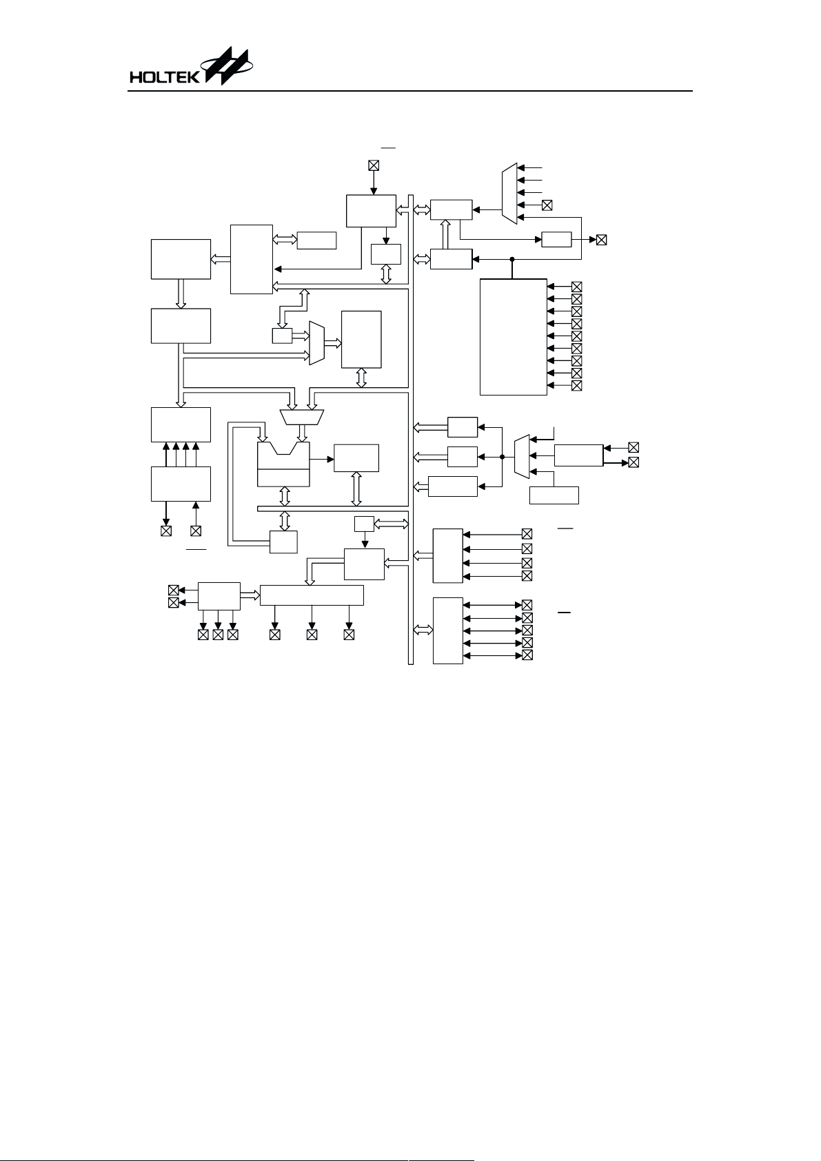
Block Diagram
HT47C20
Program
ROM
Instructio n
R egister
Instructio n
D ecoder
Tim ing
G enerator
OSC2
C1
C2
OSC1
RES
VDD
VSS
Voltage
V1 V2 V3
Halve
Program
C ounter
MP
ALU
S h ifte r
ACC
COM 0~
COM 2
STACK
M
U
X
MUX
LCD Driver
COM 3/
SEG19
PB0/INT
Interrupt
Circuit
DATA
Memory
STATUS
BP
LC D
Memory
SEG0~
SEG18
IN T C
Tim er A
Tim er B
RTC
WDT
Tim e Base
PB
PA
M
U
X
O verflow
RC Type
A/D C onverter
Port B
Port A
System C lock
T1
RTC Output
PFD
A/D Clock
SYS CLK/4
M
U
X
WDT OSC
PB0/IN T
PB1
PB2/TM R
PB3
PA0/BZ
PA1/BZ
PA2/IR
PA3/PFD
PA4~PA7
PB2/TMR
IN 0
CS0
RS0
CRT0
RT0
IN 1
CS1
RS1
RT1
RTC OSC
PA3/PFD
OSC3
OSC4
2 January 18, 2000
Page 3

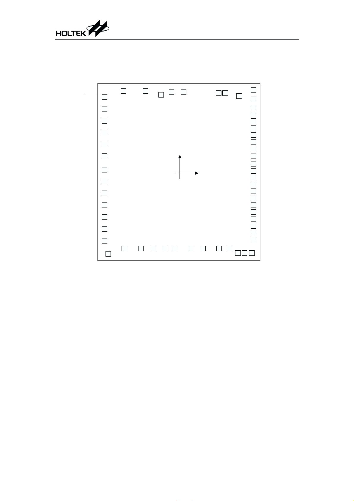
Pin Assignment
NC
NC
RES
HT47C20
OSC4
OSC3
OSC2
OSC1
VDD
C1
C2
V1
V2
V3
PA0/BZ
PA1/BZ
PA2/IR
PA3/PFD
PA4
PA5
PA6
PA7
PB0/IN T
PB1
PB2/TM R
PB3
NC
NC
NC
NC
NC
NC
VSS
1
2
3
4
5
6
7
8
9
10
11
12
13
14
15
16
17
18
19
20 21 22 23 24 25 26 27 28 29 30 31 32
RT1
61 60 59 58 57 56 55 54 53 5264 63 62
HT47C20
64 Q FP
RS1
CS1
IN 1
CRT0
RT0
RS0
CS0
IN 0
COM 0
COM 1
SEG0
51
SEG1
50
SEG2
49
SEG3
48
SEG4
47
SEG5
46
SEG6
45
SEG7
44
SEG8
43
SEG9
42
SEG10
41
SEG11
40
SEG12
39
SEG13
38
SEG14
37
36
SEG15
35
SEG16
34
SEG17
33
SEG18
COM 2
COM 3/SEG19
3 January 18, 2000
Page 4
Pad Assignment
MCLR
PA0
PA1
PA2
PA3
PA4
PA5
PA6
PA7
PB0
PB1
PB2
PB3
VSS
HT47C20
OSC3
OSC1
56
1
2
3
4
5
6
7
8
9
10
11
12
13
15431644174518
14
RT1
OSC2
VDD
55
54
RS1
CS1
IN 1
OSC4
C2
C1
(0 , 0 )
20
19
RT0
CRT0
22
21
RS0
CS0
502351
IN 0
V1
49
2452255326
COM 0
COM 1
V2
48
47
V3
SEG 0
46
SEG 1
SEG 2
SEG 3
42
SEG 4
41
SEG 5
40
SEG 6
SEG 7
39
38
SEG 8
SEG 9
37
36
SEG 10
35
SEG 11
SEG 12
34
SEG 13
33
32
SEG 14
SEG 15
31
30
SEG 16
29
SEG 17
SEG 18
28
27
COM 3
COM 2
* The IC substrate should be connected to VSS in the PCB layout artwork.
4 January 18, 2000
Page 5
Pad Description
HT47C20
Pad No. Pad Name I/O
1 RES
2
3
4
5
6~9
10
11
12
13
14 VSS
18
17
16
15
23
22
21
20
19
27
26~24
28~46 SEG18~SEG0 O
49, 48, 47
51, 50
52
53
PA0/BZ
PA1/BZ
PA2/IR
PA3/PFD
PA4~PA7
PB0/INT
PB1
PB2/TMR
PB3
IN1
CS1
RS1
RT1
IN0
CS0
RS0
CRT0
RT0
SEG19/COM3
COM2~COM0
V1, V2, V3
C1, C2
OSC4
OSC3
I/O
¾¾
¾¾
I
I
I
O
O
O
I
O
O
O
O
O
O
I
Mask
Option
¾
Wake-up
Pull-high
or None
CMOS or
NMOS
¾
¾
¾
1/3 or 1/4
Duty
¾
¾
Function
Schmitt trigger reset input. Active low.
Bidirectional 8-bit input/output port. The low nibble
of the PA can be configured as CMOS output or
NMOS output with or without pull-high resistors
(mask option). NMOS output can be configured as
schmitt trigger input with or without pull-high resis
tors. Each bit of NMOS output can be configured as
wake up input by mask option. Of the eight bits,
PA0~PA1 can be set as I/O pins or buzzer outputs by
mask option. PA2 can be set as an I/O pin or an IR
carrier output also by mask option. PA3 can be set as
an I/O pin or a PFD output also by mask option.
Four-bit Schmitt trigger input port. The PB is config
ured as with pull-high resistors. Of the four bits, PB0
can be set as an input pin or an external interrupt in
put pin (INT
be set as an input pin or a timer/event counter input
pin also by software application.
Negative power supply, GND
Oscillation input pin of channel 1
Reference capacitor connection pin of channel 1
Reference resistor connection pin of channel 1
Resistor sensor connection pin for measurement of
channel 1
Oscillation input pin of channel 0
Reference capacitor connection pin of channel 0
Reference resistor connection pin of channel 0
Resistor/capacitor sensor connection pin for measurement of channel 0
Resistor sensor connection pin for measurement of
channel 0
SEG19/COM3 can be set as a segment or a common
output driver for LCD panel by mask option.
COM2~COM0 are outputs for LCD panel plate.
LCD driver outputs for LCD panel segments
Voltage pump
Real time clock oscillators
) by software application. While PB2 can
-
-
-
5 January 18, 2000
Page 6

HT47C20
Pad No. Pad Name I/O
54 VDD
55
56
OSC2
OSC1
Mask
Option
¾¾
Positive power supply
Function
OICrystal orRCOSC1 and OSC2 are connected to an RC network or a
crystal (by mask option) for the internal system clock.
Absolute Maximum Ratings
Supply Voltage ..............................-0.3V to 5.5V
Storage Temperature.................-50°Cto125°C
Note: These are stress ratings only. Stresses exceeding the range specified under ²Absolute Maxi
mum Ratings² may cause substantial damage to the device. Functional operation of this de
vice at other conditions beyond those listed in the specification is not implied and prolonged
exposure to extreme conditions may affect device reliability.
D.C. Characteristics
Symbol Parameter
V
I
I
DD1
DD2
Operating Voltage
DD
Operating Current
(Crystal OSC)
Operating Current (RC OSC) 3V
Standby Current
I
STB1
(32.768kHz Crystal Oscillator
Enable, LCD Off)
Standby Current
I
STB2
(32.768kHz Crystal Oscillator
Enable, LCD On)
Standby Current
I
STB3
(Watchdog RC Oscillator
Enable, LCD Off)
Standby Current
I
STB4
(Watchdog RC Oscillator
Enable, LCD On)
Standby Current
I
STB5
(32.768kHz Crystal and
Watchdog RC Oscillator Both
Disabled, LCD Off)
V
DD
¾¾
3V
3V No load, system Halt
3V No load, system Halt
3V No load, system Halt
3V No load, system Halt
3V No load, system Halt
Input Voltage .................V
-0.3V to VDD+0.3V
SS
Operating Temperature ..............-40°Cto85°C
Test Conditions
Conditions
Min. Typ. Max. Unit
2.4 3 3.6 V
No load, f
A/D Off
No load, f
A/D Off
SYS
=455kHz
SYS
=455kHz
0.2 0.4 mA
¾
0.2 0.4 mA
¾
¾¾
¾¾
¾¾
¾¾
¾¾
3
5
7
10
1
Ta=25°C
mA
mA
mA
mA
mA
-
-
6 January 18, 2000
Page 7

HT47C20
Symbol Parameter
I
STB6
V
V
V
V
V
I
OL
I
OH
I
OL1
I
OH1
I
OL2
I
OH2
I
OL3
I
OH3
I
OL4
I
OH4
I
OL5
I
OH5
R
Standby Current
(A/D On, *R=5kW, *f=500kHz)
Input Low Voltage for I/O
IL1
Ports
Input High Voltage for I/O
IH1
Ports
Input Low Voltage (RES)3V
IL2
Input Low Voltage (INT, TMR) 3V
IL3
Input High Voltage
IH2
(RES
, INT, TMR)
I/O Port Sink Current 3V
I/O Port Source Current 3V
Common 0~3 Output Sink
Current
Common 0~3 Output Source
Current
Segment 0~19 Output Sink
Current
Segment 0~19 Output Source
Current
Common 0~3 Output Sink
Current
Common 0~3 Output Source
Current
Segment 0~19 Output Sink
Current
Segment 0~19 Output Source
Current
RC Oscillation Output Sink
Current
RC Oscillation Output Source
Current
Pull-high Resistance of I/O
PH
Ports and INT
Test Conditions
V
DD
Conditions
3V No load, system Halt
3V
3V
3V
3V
3V
3V
3V
3V
3V
3V
3V
3V
3V
3V
0.5V
0.3V
0.8V
V
=0.3V
OL
V
OH
=0.3V (1/2 bias)
V
OL
V
OH
=0.3V (1/2 bias)
V
OL
V
OH
=0.45V (1/3 bias)
V
OL
V
OH
=0.45V (1/3 bias)
V
OL
V
OH
=0.3V
V
OL
V
OH
¾
¾
DD
DD
DD
=2.7V
=2.7V (1/2 bias)
=2.7V (1/2 bias)
=4.05V (1/3 bias)
=4.05V (1/3 bias)
=2.7V
¾
Min. Typ. Max. Unit
600 1200
¾
0
¾
2.1
¾
0
¾
0
¾
2.4
¾
2 3.5
-1 -1.5 ¾
50 100
mA
0.9 V
3V
1.5 V
0.9 V
3V
mA
¾
mA
¾mA
-50 -100 ¾mA
15 30
¾mA
-15 -30 ¾mA
100 180
¾mA
-100 -180 ¾mA
20 40
¾mA
-20 -40 ¾mA
510
-5 -10 ¾
40 60 80
¾
mA
mA
kW
Note: *R means the resistance of RC type A/D converter
*f means the frequency of RC type A/D converter
7 January 18, 2000
Page 8
HT47C20
A.C. Characteristics
Symbol Parameter
f
SYS1
f
SYS2
f
TIMER
t
WDTOSC
t
RES
t
SST
t
INT
f
AD
Note: t
System Clock (Crystal OSC) 3V
System Clock (RC OSC) 3V
Timer I/P Frequency (TMR) 3V
Watchdog Oscillator 3V
External Reset Low Pulse Width
System Start-up Timer Period
Interrupt Pulse Width
A/D Converter Frequency 3V
=1/f
SYS
SYS
Test Conditions
V
DD
Conditions
¾
¾
¾
¾
¾¾
Power-up or
¾
wake-up from halt
¾¾
¾¾¾
Ta=25°C
Min. Typ. Max. Unit
455
64
0
45 90 180
10
1024
¾
10
480 kHz
¾
500 kHz
¾
500 kHz
¾
ms
¾¾ms
t
¾
SYS
¾¾ms
500 kHz
8 January 18, 2000
Page 9

Functional Description
HT47C20
Execution flow
The system clock for the HT47C20 is derived
from either a crystal or an RC oscillator. The
system clock is internally divided into four
non-overlapping clocks. One instruction cycle
consists of four system clock cycles.
Instruction fetching and execution are
pipelined in such a way that a fetch takes one
instruction cycle while decoding and execution
takes the next instruction cycle. However, the
pipelining scheme causes each instruction to ef
fectively execute in one cycle. If an instruction
changes the program counter, two cycles are re
quired to complete the instruction.
Program counter - PC
The 11-bit program counter (PC) controls the
sequence in which the instructions stored in the
program ROM are executed and its contents
specify a maximum of 2048 addresses.
After accessing a program memory word to
fetch an instruction code, the contents of the
program counter are incremented by one. The
program counter then points to the memory
word containing the next instruction code.
When executing a jump instruction, conditional
skip execution, loading PCL register, subroutine call, initial reset, internal interrupt, external interrupt or return from subroutine, the PC
manipulates the program transfer by loading
the address corresponding to each instruction.
The conditional skip is activated by instruction.
Once the condition is met, the next instruction,
fetched during the current instruction execu
tion, is discarded and a dummy cycle replaces it
to get the proper instruction. Otherwise pro
ceed with the next instruction.
The lower byte of the program counter (PCL) is
a readable and writeable register (06H).
Moving data into the PCL performs a short
jump. The destination will be within 256 loca
-
tions.
When a control transfer takes place, an addi
tional dummy cycle is required.
Program memory - ROM
The program memory is used to store the pro
gram instructions which are to be executed. It
also contains data, table, and interrupt entries,
and is organized into 2048´16 bits, addressed
by the program counter and table pointer.
Certain locations in the program memory are
reserved for special usage
·
Location 000H
This area is reserved for the initialization
program. After chip reset, the program always begins execution at location 000H.
·
Location 004H
This area is reserved for the external inter-
rupt service program. If the INT
activated, and the interrupt is enabled and
-
-
-
-
-
input pin is
S ystem C lock
Instructio n C lock
PC
T1 T2 T3 T4 T1 T2 T3 T4 T1 T2 T3 T4
PC PC+1 PC+2
F e tc h IN S T (P C )
E xecute IN S T (P C -1 )
F e tc h IN S T (P C + 1 )
E xecute IN S T (P C )
F e tc h IN S T (P C + 2 )
E xecute IN S T (P C + 1)
Execution flow
9 January 18, 2000
Page 10
HT47C20
m
the stack is not full, the program begins exe
cution at location 004H.
·
Location 008H
This area is reserved for the time base interrupt
service program. If time base interrupt results
from a time base overflow, and if the interrupt is
enabled and the stack is not full, the program
begins execution at location 008H.
·
Location 00CH
This area is reserved for the real time clock in
terrupt service program. If a real time clock
interrupt results from a real time clock over
-
000H
004H
008H
00C H
010H
-
n00H
nFF H
-
D evice initialization program
External interrupt subroutine
T im e b a s e in te rru p t s u b ro u tin e
R T C interrupt subroutine
Tim er/event counter interrupt subroutine
Look-up table (256 w ords)
Progra
ROM
flow, and if the interrupt is enabled and the
stack is not full, the program begins execution
at location 00CH.
·
Location 010H
This area is reserved for the timer/event coun
ter interrupt service program. If a timer inter
rupt results from a timer/event counter A or B
overflow, and if the interrupt is enabled and
the stack is not full, the program begins exe
cution at location 010H.
·
Table location
Any location in the ROM space can be used as
look up tables. The instructions TABRDC [m]
(the current page, 1 page=256 words) and
TABRDL [m] (the last page) transfer the contents of the lower-order byte to the specified
Mode
*10 *9 *8 *7 *6 *5 *4 *3 *2 *1 *0
7FFH
-
-
-
data memory, and the higher-order byte to
TBLH (08H). Only the destination of the
lower-order byte in the table is well-defined,
the higher-order byte of the table word are
transferred to the TBLH. The table
higher-order byte register (TBLH) is read
only. The table pointer (TBLP) is a read/write
register (07H), which indicates the table location. Before accessing the table, the location
Look-up table (256 w ords)
16 bits
N ote: n ranges from 0 to 7
Program memory
Program Counter
Initial reset 00000000000
External interrupt 00000000100
Time base interrupt 00000001000
RTC interrupt 00000001100
Timer/event counter interrupt 00000010000
Skip PC+2
Loading PCL *10 *9 *8 @7 @6 @5 @4 @3 @2 @1 @0
Jump, call branch #10 #9 #8 #7 #6 #5 #4 #3 #2 #1 #0
Return from subroutine S10 S9 S8 S7 S6 S5 S4 S3 S2 S1 S0
Program counter
Note: *10~*0: Program counter bits #10~#0: Instruction code bits
S10~S0: Stack register bits @7~@0: PCL bits
10 January 18, 2000
Page 11

HT47C20
must be placed in TBLP. The TBLH is read
only and cannot be restored. If the main rou
tine and the ISR (Interrupt Service Routine)
both employ the table read instruction, the
contents of the TBLH in the main routine are
likely to be changed by the table read instruc
tion used in the ISR. Errors can occur. In
other words, using the table read instruction
in the main routine and the ISR simulta
neously should be avoided. However, if the ta
ble read instruction has to be applied in both
the main routine and the ISR, the interrupt is
supposed to be disabled prior to the table read
instruction. It will not be enabled until the
TBLH has been backed up. All table related
instructions need two cycles to complete the
operation. These areas may function as nor
mal program memory depending upon the re
quirements.
Stack register - STACK
This is a special part of the memory which is
used to save the contents of the program coun
ter (PC) only. The stack is organized into four
levels and is neither part of the data nor part of
the program space, and is neither readable nor
writeable. The activated level is indexed by the
stack pointer (SP) and is neither readable nor
writeable. At a subroutine call or interrupt acknowledgment, the contents of the program
counter are pushed onto the stack. At the end of a
subroutine or an interrupt routine, signaled by
a return instruction (RET or RETI), the program counter is restored to its previous value
from the stack. After a chip reset, the SP will
point to the top of the stack.
If the stack is full and a non-masked interrupt
takes place, the interrupt request flag will be
Instruction(s)
TABRDC [m] P10 P9 P8 @7 @6 @5 @4 @3 @2 @1 @0
TABRDL [m] 1 1 1 @7 @6 @5 @4 @3 @2 @1 @0
*10 *9 *8 *7 *6 *5 *4 *3 *2 *1 *0
recorded but the acknowledgment will be inhib
ited. When the stack pointer is decremented (by
RET or RETI), the interrupt will be serviced.
This feature prevents stack overflow allowing
the programmer to use the structure more eas
ily. In a similar case, if the stack is full and a
²CALL² is subsequently executed, stack over
flow occurs and the first entry will be lost (only
-
the most recent four return addresses are
-
stored).
Data memory - RAM
The data memory is designed with 83 ´ 8 bits.
The data memory and is divided into two func
tional groups: special function registers and
general purpose data memory (64´ 8). Most are
read/write, but some are read only.
The special function registers include the indi
rect addressing register 0 (00H), the memory
pointer register 0 (mp0; 01H), the indirect ad
dressing register 1 (02H), the memory pointer
register 1 (MP1;03H), the bank pointer
(BP;04H), the accumulator (ACC;05H), the pro
gram counter lower-order byte register
(PCL;06H), the table pointer (TBLP;07H), the
table higher-order byte register (TBLH;08H),
the real time clock control register (RTCC;09H),
the status register (STATUS;0AH), the interrupt control register 0(INTC0;0BH), the I/O registers (PA;12H, PB;14H), the interrupt control
register 1 (INTC1;1EH), the timer/event counter
A higher order byte register (TMRAH; 20H), the
timer/event counter A lower order byte register
(TMRAL; 21H), the timer/event counter control
register (TMRC; 22H), the timer/event counter B
higher order byte register (TMRBH; 23H), the
timer/event counter B lower order byte register
(TMRBL; 24H), and the RC oscillator type A/D
Table Location
-
-
-
-
-
-
-
Table location
Note: *10~*0: Table location bits @7~@0: Table pointer bits
P10~P8: Current program counter bits
11 January 18, 2000
Page 12

HT47C20
Indirect A ddressing R egister 0
00H
01H
Indirect A ddressing R egister 1
02H
03H
04H
05H
06H
07H
08H
09H
0AH
0BH
0C H
0D H
0EH
0FH
10H
11H
12H
13H
14H
15H
16H
17H
18H
19H
1AH
1BH
1C H
1D H
1EH
1FH
20H
21H
22H
23H
24H
25H
26H
40H
7FH
RTCC
STATUS
IN T C 0
IN T C 1
TM RA H
TM RA L
TM RC
TM RB H
TM RB L
ADCR
G eneral Purpose
D ata M em ory
(64 B ytes)
MP 0
MP1
BP
ACC
PCL
TBLP
TBLH
PA
PB
Special Purpose
D ata M em ory
: U n u s e d
R ead as "00"
converter control register (ADCR; 25H). The re
maining space before the 40H are reserved for fu
ture expanded usage and reading these location
will return the result 00H. The general purpose
data memory, addressed from 40H to 7FH, is
used for data and control information under in
struction command.
All data memory areas can handle arithme
tic, logic, increment, decrement and rotate
operations. Except for some dedicated bits,
each bit in the data memory can be set and re
set by the SET [m].i and CLR [m].i instruc
tion, respectively. They are also indirectly
accessible through memory pointer registers
(MP0;01H, MP1;03H).
Indirect addressing register
Location 00H and 02H are indirect addressing
registers that are not physically implemented.
Any read/write operation of [00H] and [02H] ac
cess data memory pointed to by MP0 (01H) and
MP1 (03H) respectively. Reading location 00H
or 02H indirectly will return the result 00H.
Writing indirectly results in no operation.
The function of data movement between two in
direct addressing registers are not supported.
The memory pointer registers, MP0 and MP1,
are both 8-bit registers which can be used to access the data memory by combining corresponding indirect addressing registers.
Only MP0 can be applied to data memory, while
MP1 can be applied to data memory and LCD
display memory.
Accumulator
The accumulator is closely related to ALU op
erations. It is also mapped to location 05H of
the data memory and is capable of carrying out
immediate data operations. The data move
ment between two data memory locations
must pass through the accumulator.
-
-
-
-
-
-
-
-
-
-
RAM mapping (bank 0)
12 January 18, 2000
Page 13

HT47C20
Arithmetic and logic unit - ALU
This circuit performs 8-bit arithmetic and logic
operation. The ALU provides the following
functions:
·
Arithmetic operations (ADD, ADC, SUB,
SBC, DAA)
·
Logic operations (AND, OR, XOR, CPL)
·
Rotation (RL, RR, RLC, RRC)
·
Increment and Decrement (INC, DEC)
·
Branch decision (SZ, SNZ, SIZ, SDZ ....)
The ALU not only saves the results of a data op
eration but can change the status register.
TO or PD flags. In addition it should be noted
that operations related to the status register
may give different results from those intended.
The TO and PD flags can only be changed by
the watchdog timer overflow, system power-up,
clearing the watchdog timer and executing the
HALT instruction.
The Z, OV, AC and C flags generally reflect the
status of the latest operations.
In addition, on entering the interrupt sequence
or executing the subroutine call, the status reg
ister will not be pushed onto the stack automat
ically. If the contents of the status are
important and if the subroutine can corrupt the
Status register - STATUS
This 8-bit register (0AH) contains the zero flag (Z),
carry flag (C), auxiliary carry flag (AC),
overflow flag (OV), power down flag (PD) and
watchdog time-out flag (TO). It also records the
status information and controls the operation se
quence.
With the exception of the TO and PD flags, bits
in the status register can be altered by instruc
tions like most other registers. Any data writ
ten into the status register will not change the
status register, precautions must be taken to
save it properly.
Interrupts
The HT47C20 provides an external interrupt,
an internal timer/event counter interrupt, an
internal time base interrupt, and an internal
real time clock interrupt. The interrupt control
register 0 (INTC0;0BH) and interrupt control
register 1 (INTC1;1EH) both contain the inter
rupt control bits to set the enable/disable and
interrupt request flags.
Labels Bits Function
C is set if the operation results in a carry during an addition operation or if a bor-
C0
row does not take place during a subtraction operation; otherwise C is cleared. C
is also affected by a rotate through carry instruction.
AC is set if the operation results in a carry out of the low nibbles in addition or no
AC 1
borrow from the high nibble into the low nibble in subtraction; otherwise AC is
cleared.
Z2
OV 3
PD 4
TO 5
¾
¾
Z is set if the result of an arithmetic or logic operation is zero; otherwise Z is
cleared.
OV is set if the operation results in a carry into the highest-order bit but not a
carry out of the highest-order bit, or vice versa; otherwise OV is cleared.
PD is cleared when either a system power-up or executing the CLR WDT in
struction. PD is set by executing the HALT instruction.
TO is cleared by a system power-up or executing the CLR WDT or HALT in
struction. TO is set by a WDT time-out.
6
Undefined, read as ²0²
7
Undefined, read as ²0²
-
-
-
-
-
STATUS register
13 January 18, 2000
Page 14

HT47C20
Once an interrupt subroutine is serviced, all
other interrupts will be blocked (by clearing the
EMI bit). This scheme may prevent any further
interrupt nesting. Other interrupt requests
may happen during this interval, but only the
interrupt request flag is recorded. If a certain
interrupt needs servicing within the service
routine, the EMI bit and the corresponding bit
of INTC0 or INTC1 may be set allow interrupt
nesting. If the stackis full, the interrupt request
will not be acknowledged, even if the related in
terrupt is enabled, until the SP is decremented.
If immediate service is desired, the stack must
Register Bit No. Label Function
Control the master (global) interrupt
(1= enabled; 0= disabled)
Control the external interrupt
(1= enabled; 0= disabled)
Control the time base interrupt
(1= enabled; 0= disabled)
Control the real time clock interrupt
(1= enabled; 0= disabled)
External interrupt request flag
(1= active; 0= inactive)
Time base request flag
(1= active; 0= inactive)
Real time clock request flag
(1= active; 0= inactive)
Control the timer/event counter interrupt
(1= enabled; 0=disabled)
Internal timer/event counter request flag
(1= active; 0= inactive)
INTC0
(0BH)
INTC1
(1EH)
0 EMI
1 EEI
2 ETBI
3 ERTI
4 EIF
5 TBF
6 RTF
7
0 ETI
1
2
3
4TF
5
6
7
¾ Unused bit, read as ²0²
¾ Unused bit, read as ²0²
¾ Unused bit, read as ²0²
¾ Unused bit, read as ²0²
¾ Unused bit, read as ²0²
¾ Unused bit, read as ²0²
¾ Unused bit, read as ²0²
be prevented from becoming full.
All these kinds of interrupt have a wake-up ca
pability. As an interrupt is serviced, a control
transfer occurs by pushing the program counter
onto the stack and then by branching to subrou
tines at specified location(s) in the program
memory. Only the program counter is pushed
onto the stack. If the contents of the register
and status register (STATUS) is altered by the
interrupt service program which corrupts the
desired control sequence, the contents must be
saved first.
-
-
INTC register
14 January 18, 2000
Page 15

HT47C20
External interrupt is triggered by a high to low
transition of INT
quest flag (EIF; bit 4 of INTC0) will be set.
When the interrupt is enabled, and the stack is
not full and the external interrupt is active, a
subroutine call to location 04H will occur. The
interrupt request flag (EIF) and EMI bits will
be cleared to disable other interrupts.
The internal timer/event counter interrupt is
initialized by setting the timer/event counter
interrupt request flag (TF; bit 4 of INTC1),
caused by a timer A or timer B overflow. When
the interrupt is enabled, and the stack is not
full and the TF bit is set, a subroutine call to lo
cation 10H will occur. The related interrupt re
quest flag (TF) will be reset and the EMI bit
cleared to disable further interrupts.
The time base interrupt is initialized by setting
the time base interrupt request flag (TBF; bit 5
of INTC0), caused by a regular time base sig
nal. When the interrupt is enabled, and the
stack is not full and the TBF bit is set, a subrou
tine call to location 08H will occur. The related
interrupt request flag (TBF) will be reset and
the EMI bit cleared to disable further inter
rupts.
The real time clock interrupt is initialized by
setting the real time clock interrupt request
flag (RTF; bit 6 of INTC0), caused by a regular
real time clock signal. When the interrupt is enabled, and the stack is not full and the RTF bit
is set, a subroutine call to location 0CH will occur. The related interrupt request flag (RTF)
will be reset and the EMI bit cleared to disable
further interrupts.
During the execution of an interrupt subrou
tine, other interrupt acknowledgments are held
until the RETI instruction is executed or the
EMI bit and the related interrupt control bit
are set to 1 (if the stack is not full). To return
from the interrupt subroutine, RET or RETI in
struction may be invoked. RETI will set the
EMI bit to enable an interrupt service, but RET
does not.
and the related interrupt re
Interrupts occurring in the interval between
the rising edges of two consecutive T2 pulses,
will be serviced on the latter of the two T2
pulses, if the corresponding interrupts are en
abled. In the case of simultaneous requests the
following table shows the priority that is ap
plied. These can be masked by resetting the
EMI bit.
No. Interrupt Source Priority Vector
a External interrupt 1 04H
b Time base interrupt 2 08H
-
-
-
-
-
-
-
Real time clock
c
interrupt
Timer/event counter
d
interrupt
The external interrupt request flag (EIF), real
time clock interrupt request flag (RTF), time base
interrupt request flag (TBF), enable external in
terrupt bit (EEI), enable real time clock interrupt
bit (ERTI), enable time base interrupt bit (ETBI),
and enable master interrupt bit (EMI) constitute
an interrupt control register 0 (INTC0) which is
located at 0BH in the data memory. The
timer/event counter interrupt request flag (TF),
enable timer/event counter interrupt bit (ETI) on
the other hand, constitute an interrupt control
register 1 (INTC1) which is located at 1EH in the
data memory. EMI, EEI, ETI, ETBI, and ERTI
are used to control the enabling/disabling of interrupts. These bits prevent the requested interrupt being serviced. Once the interrupt request
flags (RTF, TBF, TF, EIF) are set, they remain in
the INTC1 or INTC0 respectively until the interrupts are serviced or cleared by a software in
struction.
It is recommended that a program does not use
the ²CALL subroutine² within the interrupt
subroutine. Because interrupts often occur in
an unpredictable manner or need to be serviced
immediately in some applications, if only one
stack is left, and enabling the interrupt is not
well controlled, once the ²CALL subroutine² op
erates in the interrupt subroutine will damage
the original control sequence.
3 0CH
4 10H
-
-
-
-
-
15 January 18, 2000
Page 16

HT47C20
Oscillator configuration
There are two oscillator circuits in the HT47C20.
OSC1
OSC2
C ry s t a l O s c illa t o r R C O s c illa to r
OSC1
OSC2
System oscillator
Both are designed for system clocks; the RC oscil
lator and the crystal oscillator, which are deter
mined by mask option. No matter what oscillator
type is selected, the signal provides the system
clock. The halt mode stops the system oscillator
and ignores an external signal to conserve power.
The OSC1 and OSC2 are at the same level
when the system enters the power down mode.
If an RC oscillator is used, an external resistor
between OSC1 and OSC2 is need and the resis
tance must range from 51kW to 1MW. The RC
oscillator provides the most cost effective solu
tion. However, the frequency of the oscillation
may vary with VDD, temperature and the chip
itself due to process variations. It is, therefore,
not suitable for timing sensitive operations
where accurate oscillator frequency is desired.
If a crystal oscillator is used, a crystal across
OSC1 and OSC2 is needed to provide the feedback and phase shift needed for oscillator, no
other external components are needed. Instead
of a crystal, a resonator can also be connected
between OSC1 and OSC2 to get a frequency reference, but two external capacitors in OSC1
and OSC2 are required.
There is another oscillator circuit designed for
the real time clock. In this case, only the
32768kHz crystal oscillator can be applied. The
crystal should be connected between OSC3 and
OSC4, and two external capacitors along with
one external resistor are required for the oscil
lator circuit in order to get a stable frequency.
The RTC oscillator circuit can be controlled to
oscillate quickly by setting ²SAVE² bit (bit 4 of
RTCC) to ²0². After power on reset, the ²SAVE²
bit initial value is ²0 ² that is on the
quick-oscillate mode. It¢s recommended to turn
it off by setting the ²SAVE² bit ²1² after a period
ofabout2secondstoavoiddrainingextrapower.
OSC3
32768H z
OSC4
RTC oscillator
The WDT oscillator is a free running on-chip
-
RC oscillator, and no external components are
-
required. Even if the system enters the power
down mode, the system clock is stopped, but the
WDT oscillator still works with a period of ap
proximately 90ms. The WDT oscillator can be
disabled by mask option to conserve power.
Watchdog timer - WDT
The clock source of the WDT(f
by a dedicated RC oscillator (WDT oscillator) or
a instruction clock (system clock divided by 4)
or a real time clock oscillator (RTC oscillator),
) is implemented
s
decided by mask options. The timer is designed
to prevent a software malfunction or sequence
jumping to an unknown location with unpredictable results. The watchdog timer can be disabled by a mask option. If the watchdog timer is
disabled, all the executions related to the WDT
result in no operation.
If the clock source of WDT chooses the internal
WDT oscillator, the time-out period may vary
with temperature, VDD, and process variations. On the other hand, if the clock source selects the instruction clock and the ²HALT²
instruction is executed, WDT may stop count
ing and lose its protecting purpose, and the
logic can only be restarted by external logic.
When the device operates in a noisy environ
ment, using the on-chip RC oscillator (WDT
OSC) is strongly recommended, since the HALT
can cease the system clock.
The WDT overflow under normal operation will
initialize ²chip reset² and set the status bit TO.
Whereas in the halt mode, the overflow will ini
tialize a ²warm reset² only the PC and SP are
reset to zero. To clear the contents of WDT, three
-
-
-
-
16 January 18, 2000
Page 17
HT47C20
methods are adopted, external reset (a low level
to RES), software instruction, or a HALT instruc
tion. The software instructions are of two types
which include CLR WDT and the other set - CLR
WDT1 and CLR WDT2. Of these two types of in
struction, only one can be active depending on
the mask option -²CLR WDT times selection op
tion².Ifthe²CLR WDT² is selected (i.e., CLR
WDT times equal one), any execution of the CLR
WDT instruction will clear the WDT. In case ²CLR
WDT1² and ²CLR WDT2² are chosen (i.e. CLR
WDT times equal two), these two instructions
must be executed to clear the WDT; otherwise,
the WDT may reset the chip because of
time-out.
The WDT time-out period ranges from
15
16
~f
f
s/2
. Because the ²CLR WDT² or ²CLR
s/2
WDT1² and ²CLRWDT2² instruction only clear
the last two-stage of the WDT.
Multi-function timer
The HT47C20 provides a multi-function timer
for WDT, time base and real time clock but with
different time-out periods. The multi-function
timer consists of a 7-stage divider and an 8-bit
prescaler, with the clock source coming from
WDT OSC or RTC OSC or the instruction clock
(i.e., system clock divided by 4). The
multi-function timer also provides a selectable
frequency signal (ranges from f
LCD driver circuits, and a selectable frequency
signal (ranges from f
put by mask option. It is recommended to select
-
/22to fs/29) for buzzer out
s
/22to fs/28) for
s
a near 4kHz signal for LCD driver circuits for
proper display.
Time base
The time base offers a periodic time-out period
to generate a regular internal interrupt. Its
time-out period ranges from f
/212to fs/215se
s
lected by mask option. If time base time-out oc
curs, the related interrupt request flag (TBF;
bit 5 of INTC0) is set. But if the interrupt is en
abled, and the stack is not full, a subroutine call
to location 08H occurs.
When the HALT instruction is executed, the
time base still works (if WDT clock source co
mes from WDT RC OSC or RTC OSC) and can
wake up from halt mode.
If the TBF is set ²1² before entering the halt
mode, the wake up function will be disable.
-
-
-
-
-
S ystem C lock/4
RTC
32768H z
OSC
WDT
12kHz
OSC
Mask
Option
Selection
f
s
f
s
D ivider
D ivider
Tim e Base Interrupt
f
s
8
fs/2
Watchdog timer
8
fs/2
Mask Option
/2 ~ fs/2
12 15
Time base
Prescaler
W D T C lear
Prescaler
CK TRCK T
LC D D river
Buzzer
2
f
s
/2 ~ fs/2
fs/2 ~ fs/2
9
R
2
Tim e-out R eset
f
/2 ~ fs/2
s
8
15 16
17 January 18, 2000
Page 18

8
RT2
RT1
RT0
fs/2
f
s
D ivider
Real time clock
Real time clock - RTC
The real time clock (RTC) is operated in the
same manner as the time base that is used to
supply a regular internal interrupt. Its
time-out period ranges from f
/28to fs/215by
s
software programming . Writing data to RT2,
RT1 and RT0 (bits 2, 1, 0 of RTCC;09H) yields
various time-out periods. If the RTC time-out
occurs, the related interrupt request flag (RTF;
bit 6 of INTC0) is set. But if the interrupt is en
abled, and the stack is not full, a subroutine call
to location 0CH occurs. The real time clock
time-out signal can also be applied to be a clock
source of timer/event counter, so as to get a lon
ger time-out period.
RT2 RT1 RT0
000 2
001 2
010 2
011 2
100 2
101 2
110 2
111 2
RTC Clock Divided
Factor
8
9
10
11
12
13
14
15
Power down operation - HALT
The HALT mode is initialized by the HALT in
struction and results in the following.
·
The system oscillator will turn off but the
WDT oscillator or RTC oscillator keeps run
ning (if the WDT oscillator or the real time
clock is selected).
P re scaler
8
15
8 to 1
Mux.
·
The contents of the on-chip RAM and regis
fs/2 ~ fs/2
RTC Interrupt
ters remain unchanged.
·
The WDT will be cleared and recounted again
(if the WDT clock comes from the WDT oscil
lator or the real time clock oscillator).
·
All I/O ports maintain their original status.
·
The PD flag is set and the TO flag is cleared.
·
LCD driver is still running by mask option (if
-
the WDT OSC or RTC OSC is selected).
The system can leave the halt mode by means of
an external reset, an interrupt, an external fall
ing edge signal on port A or a WDT overflow. An
external reset causes a device initialization and
the WDT overflow performs a ²warm reset².Ex
amining the TO and PD flags, the reason for
chip reset can be determined. The PD flag is
cleared when the system power-up or executing
the CLR WDT instruction and is set when the
HALT instruction is executed. The TO flag is set
if a WDT time-out occurs, it causes a wake-up
that only resets the PC and SP, the others maintain their original status.
The port A wake-up and interrupt methods can
be considered as a continuation of normal execution. Each bit in port A can be independently
selected to wake up the device by mask option.
Awakening from an I/O port stimulus, the pro
gram will resume execution of the next instruc
tion. If awakening from an interrupt, two
sequences may happen. If the related interrupt
is disabled or the interrupt is enabled but the
stack is full, the program will resume execution
at the next instruction. If the interrupt is en
abled and the stack is not full, the regular inter
rupt response takes place.
If an interrupt request flag is set to ²1² before
entering the halt mode the wake-up function of
the related interrupt will be disabled.
HT47C20
-
-
-
-
-
-
-
-
18 January 18, 2000
Page 19

HT47C20
Once a wake-up event occurs, it takes 1024 t
SYS
(system clock period) to resume normal opera
tion. In other words, a dummy period will be in
serted after the wake-up. If the wake-up results
from an interrupt acknowledgment, the actual
interrupt subroutine execution is delayed by
one more cycle. If the wake-up results in the
next instruction execution, this will execute im
mediately after a dummy period has finished.
To minimize power consumption, all the I/O
pins should be carefully managed before enter
ing the HALT status.
Reset
·
Therearethreewaysinwhicharesetmayoccur.
·
RES reset during normal operation
·
RES reset during HALT
·
WDT time-out reset during normal operation
The WDT time-out during HALT is different
from other chip reset conditions, since it can
perform a warm reset that just resets the PC
and SP leaving the other circuits in their origi
nal state. Some registers remain unchanged
during any other reset conditions. Most regis
ters are reset to the ²initial condition² when the
reset conditions are met. By examining the PD
and TO flags, the program can distinguish between different ²chip resets².
TO PD RESET Conditions
0 0 RES
uu
0 1 RES
1u
reset during power-up
reset during normal
RES
operation
wake-up HALT
WDT time-out during normal
operation
1 1 WDT wake-up HALT
To guarantee that the system oscillator has
started and stabilized, the SST (System
Start-up Timer) provides an extra delay. There
is an extra delay of 1024 system clock pulses
when the system awakes from the HALT state
or when the system powers up.
The functional unit chip reset status are shown
below.
PC 000H
-
Interrupt Disabled
Prescaler, Divider Cleared
WDT, RTC, Time
Base
Clear. After master
reset, begin counting
Timer/event counter Off
Input/output ports Input mode
Points to the top of
the stack
t
SST
-
-
SP
VDD
RES
SST Tim e-out
C hip R eset
Reset timing chart
Note: ²u² means ²unchanged².
19 January 18, 2000
Page 20

HT47C20
V
DD
RES
HALT
RES
OSC1
WDT
10-bit R ipple
C ounter
WDT
Tim e-out
Reset
SST
W arm Reset
E xternal
Cold
Reset
Reset circuit
Power-on Detection
Reset configuration
The states of the registers are summarized in the following table:
reset
RES
(normal
operation)
RES
(HALT)
reset
WDT
time-out
(HALT)
Register
Reset
(power on)
WDT time-out
(normal
operation)
TMRAH xxxx xxxx uuuu uuuu uuuu uuuu uuuu uuuu uuuu uuuu
TMRAL xxxx xxxx uuuu uuuu uuuu uuuu uuuu uuuu uuuu uuuu
TMRC 0000 1--- 0000 1--- 0000 1--- 0000 1--- uuuu u---
TMRBH xxxx xxxx uuuu uuuu uuuu uuuu uuuu uuuu uuuu uuuu
TMRBL xxxx xxxx uuuu uuuu uuuu uuuu uuuu uuuu uuuu uuuu
ADCR 1xxx --00 1xxx --00 1xxx --00 1xxx --00 uuuu --uu
Program
Counter
000H 000H 000H 000H
000H*
MP0 xxxx xxxx uuuu uuuu uuuu uuuu uuuu uuuu uuuu uuuu
MP1 xxxx xxxx uuuu uuuu uuuu uuuu uuuu uuuu uuuu uuuu
ACC xxxx xxxx uuuu uuuu uuuu uuuu uuuu uuuu uuuu uuuu
TBLP xxxx xxxx uuuu uuuu uuuu uuuu uuuu uuuu uuuu uuuu
TBLH xxxx xxxx uuuu uuuu uuuu uuuu uuuu uuuu uuuu uuuu
STATUS --00 xxxx --1u uuuu --uu uuuu --01 uuuu --11 uuuu
INTC0 -000 0000 -000 0000 -000 0000 -000 0000 -uuu uuuu
INTC1 ---0 ---0 ---0 ---0 ---0 ---0 ---0 ---0 ---u ---u
RTCC --x0 0111 --x0 0111 --x0 0111 --x0 0111 --uu uuuu
PA 1111 1111 1111 1111 1111 1111 1111 1111 uuuu uuuu
Note:
²*² refers to ²warm reset²
²u² means ²unchanged²
²x² means ²unknown²
20 January 18, 2000
Page 21

HT47C20
Timer/event counter
One 16-bit timer/eventcounter withPFD output
or two channels of RC type A/D converter is im
plemented in the HT47C20. The ADC/TM
bit
(bit 1 of ADCRregister) decides whether timer A
and timer B is composed of one 16-bit
timer/event counter or timer Aand timer B com
posedoftwochannelsRCtypeA/Dconverter.
The TMRAL, TMRAH, TMRBL, TMRBH com
pose one 16-bit timer/event counter, when
ADC/TM
bit is ²0². The TMRBL and TMRBH
are timer/event counter preload registers for
lower-order byte and higher-order byte respec
tively.
Using the internal clock, there are three refer
ence time-base. The timer/event counter clock
source may come from the system clock or sys
tem clock/4 or RTC time-out signal or external
source.
The external clock input allows the user to count
external events, count external RC type A/D
clock, measure time intervals or pulse widths, or
generate an accurate time base.
There are six registers related to the timer/event
counter operating mode. TMRAH ([20H]),
TMRAL ([21H]), TMRC ([22H]), TMRBH ([23H]),
TMRBL ([24H]) and ADCR ([25H]). Writing
TMRBL only writes the data into a low byte
buffer, and writing TMRBH will write the data
and the contents of the low byte buffer into the
time/event counter preload register (16-bit) simultaneously. The timer/event counter preload
register is changed by writing TMRBH operations and writing TMRBL will keep the
timer/event counter preload register unchanged.
System Clock
S y s te m C lo c k /4
TM R0
A/D Clock
RTC Out
M
U
X
Reading TMRAH will also latch the TMRAL
into the low byte buffer to avoid the false timing
problem. Reading TMRAL returns the contents
of the low byte buffer. In other words, the low
byte of the timer/event counter can not be read
directly. It must read the TMRAH first to make
the low byte contents of the timer/event counter
be latched into the buffer.
The TMRC is the timer/event counter control
register, which defines the timer/event counter
options.
The timer/event counter control register de
fines the operating mode, counting enable or
disable and active edge.
Writing to timer B makes the starting value be
placed in the timer/event counter preload regis
ter, while reading timer A yields the contents of
the timer/event counter. Timer B is timer/event
counter preload register.
The TN0, TN1 and TN2 bits define the opera
tion mode. The event count mode is used to
count external events, which means that the
clock source comes from an external (TMR) pin.
The A/D clock mode is used to count external
A/D clock, the RC oscillation mode is decided by
ADCR register. The timer mode functions as a
normal timer with the clock source coming from
the internal selected clock source. Finally, the
pulse width measurement mode can be used to
count the high or low level duration of the external signal (TMR). The counting is based on
the instruction clock.
In the event count, A/D clock or internal timer
mode, once the timer/event counter starts
counting, it will count from the current con-
Data Bus
16-bit Tim er A
overflow
TQ
R
PFD
-
-
-
TN2
TN1
TN0
TO N
TE
Pulse W idth
M easurem ent
M ode Control
TN2
TN1
TN0
Timer/event counter
21 January 18, 2000
16-bit Tim er B
R eload
PA3 D ata CTRL
Page 22

HT47C20
Label
(TMRC)
¾
TE 3
TON 4
TN0
TN1
TN2
tents in the timer/event counter (TMRAH and
TMRAL) to FFFFH. Once overflow occurs, the
counter is reloaded from the timer/event coun
ter preload register (TMRBH and TMRBL) and
generates the corresponding interrupt request
flag (TF; bit 4 of INTC1) at the same time.
In the pulse width measurement mode with the
TON and TE bits are equal to one, once the
TMR has received a transient from low to high
(or high to low if the TE bit is 0) it will start
counting until the TMR returns to the original
level and resets the TON. The measured result
will remain in the timer/event counter even if
the activated transient occurs again. In other
words, only one cycle measurement can be
done. Until setting the TON, the cycle measure
ment will function again as long as it receives
further transient pulse. Note that in this opera
tion mode, the timer/event counter starts count
ing not according to the logic level but according
to the transient edges. In the case of counter
overflows, the counter is reloaded from the
timer/event counter preload register and issues
interrupt request just like the other three
modes.
To enable the counting operation, the timer ON
bit (TON; bit 4 of TMRC) should be set to 1. In
the pulse width measurement mode, the TON
Bits Function
0~2
Unused bits, read as ²0²
Defines the TMR active edge of timer/event counter
(0= active on low to high; 1= active on high to low)
Enable/disable timer counting
(0= disabled; 1= enabled)
Defines the operating mode (TN2, TN1, TN0)
000= Timer mode (system clock)
001= Timer mode (system clock/4)
010= Timer mode (RTC output)
5
011= A/D clock mode (RC oscillation decided by ADCR register)
6
100= Event counter mode (external clock)
7
101= Pulse width measurement mode (system clock/4)
110= Unused
111= Unused
TMRC register
will be automatically cleared after the measure
ment cycle is completed. But in the other three
modes, the TON can only be reset by instruc
tions. The overflow of the timer/event counter is
one of the wake-up sources and can also be ap
plied to a PFD (Programmable Frequency Divider) output at PA3 by mask option. No matter
what the operation mode is, writing a 0 to ETI
can disable the corresponding interrupt service.
When the PFD function is selected, executing
²CLR PA.3² instruction to enable PFD output
and executing ²SET PA.3² instruction to disable PFD output and PA.3 output low level.
In the case of timer/event counter OFF
condition, writing data to the timer/event counter
-
preload register also reloads that data to the
timer/event counter. But if the timer/event coun
-
ter turns on, data written to the timer/event
-
counter preload register is kept only in the
timer/event counter preload register. The
timer/event counter will still operate until
overflow occurs.
When the timer/event counter (reading
TMRAH) is read, the clock will be blocked to
avoid errors. As this may results in a counting
error, this must be taken into consideration by
the programmer.
-
-
-
-
22 January 18, 2000
Page 23

HT47C20
It is strongly recommended to load first the de
sired value for TMRBL, TMRBH, TMRAL, and
TMRAH registers, before turning on the re
lated timer/event counter for proper operation.
Because the initial value of TMRBL, TMRBH,
TMRAL and TMRAH are unknown.
Example for Timer/event counter mode (disable interrupt):
clr tmrc
clr adcr.1 ; set timer mode
clr intc1.4 ; clear timer/event counter interrupt request flag
mov a, low (65536-1000) ; give timer initial value
mov tmrbl, a ; count 1000 time and then overflow
mov a, high (65536-1000)
mov tmrbh, a
mov a, 00110000b ; timer clock source=T1 and timer on
mov tmrc, a
p10:
clr wdt
snz intcl.4 ; polling timer/event counter interrupt request flag
jmp p10
If the timer/event counter is on, the TMRAH,
TMRAL, TMRBH and TMRBL cannot be read
or written to. Only when the timer/event coun
ter is off and when the instruction ²MOV² is
used could those four registers be read or writ
ten to.
-
-
clr intcl.4 ; clear timer/event counter interrupt request flag
; program contimue
23 January 18, 2000
Page 24

HT47C20
A/D converter
Two channels of RC type A/D converter are im
plemented in the HT47C20. The A/D converter
contains two 16-bit programmable count-up
counter and the Timer A clock source may come
from the system clock, instruction clock or RTC
output. The timer B clock source may come
from the external RC oscillator. The TMRAL,
TMRAH, TMRBL, TMRBH is composed of the
A/D converter when ADC/TM
register) is ²1².
The A/D converter timer B clock source may
come from channel 0 (IN0 external clock input
mode, RS0~CS0 oscillation, RT0~CS0 oscilla
tion, CRT0~CS0 oscillation (CRT0 is a resis
tor), or RS0~CRT0 oscillation (CRT0 is a
capacitor) or channel 1 (RS1~CS1 oscillation,
RT1~CS1 oscillation or IN1 external clock in
put). The timer A clock source is from the sys
tem clock, instruction clock or RTC prescaler
clock output decided by TMRC register.
There are six registers related to the A/D con
verter, i.e., TMRAH, TMRAL, TMRC, TMRBH,
TMRBL and ADCR. The internal timer clock is
input to TMRAH and TMRAL, the A/D clock is
Label
(ADCR)
OVB/OVA
ADC/TM
¾
M0
M1
M2
M3
Bits Function
In the RC type A/D converter mode, this bit is used to define the timer/event
counter interrupt which comes from timer A overflow or timer B overflow.
0
(0= timer A overflow; 1= timer B overflow)
In the timer/event counter mode, this bit is void.
Defines 16 timer/event counters or RC type A/D converter is enabled.
1
(0= timer/event counter enable; 1= A/D converter is enabled)
2~3
Unused bits, read as ²0².
Defines the A/D converter operating mode (M3, M2, M1, M0)
0000= IN0 external clock input mode
0001= RS0~CS0 oscillation (reference resistor and reference capacitor)
0010= RT0~CS0 oscillation (resistor sensor and reference capacitor)
4
0011= CRT0~CS0 oscillation (resistor sensor and reference capacitor)
5
0100= RS0~CRT0 oscillation (reference resistor and sensor capacitor)
6
0101= RS1~CS1 oscillation (reference resistor and reference capacitor)
7
0110= RT1~CS1 oscillation (resistor sensor and reference capacitor)
0111= IN1 external clock input mode
1XXX= Undefined mode
bit (bit 1 of ADRC
input to TMRBH and TMRBL. The OVB/OVA
bit (bit 0 of ADCR register) decides whether
timer A overflows or timer B overflows, then
the TF bit is set and timer interrupt occurs.
When the A/D converter mode timer A or timer
B overflows, the TON bit is reset and stop
counting. Writing TMRAH/TMRBH makes the
starting value be placed in the timer A/timer B
and reading TMRAH/TMRBH gets the con
tents of the timer A/timer B. Writing
TMRAL/TMRBL only writes the data into a low
byte buffer, and writing TMRAH/TMRBH will
write the data and the contents of the low byte
buffer into the timer A/timer B (16-bit) simulta
neously. The timer A/timer B is changed by writ
ing TMRAH/TMRBH operations and writing
TMRAL/TMRBL will keep timer A/timer B un
changed.
Reading TMRAH/TMRBH will also latch the
TMRAL/TMRBL into the low byte buffer to avoid
the false timing problem. ReadingTMRAL/TMRBL
returns the contents of thelow byte buffer. In other
word, the low byte of timer A/timer B can not be
read directly. It must read the TMRAH/TMRBH
first to make the low byte contents of timer A/timer
Bbelatchedinto the buffer.
-
-
-
-
ADCR register
24 January 18, 2000
Page 25

S ystem C lock
S ystem C lock/4
RTC Output
S1
S2
S3
Tim er A
TO N
Tim er B
HT47C20
OVB/OVA=0
Interrupt
OVB/OVA=1
Reset TON
S12
S13
S4
TN2
TN1
TN0
0
0
0
Other
N ote: 0=off, 1=on
0
0
0
1
1
0
S5
CS0IN 0
S1
1
0
0
0
S6 S7
CRT0
S2
S3
0
1
0
0
M3
0
0
0
0
1
0
0
0
0
0
0
0
1
N ote: 0=off, 1=on
RS0S8RT0
M1
M2
0
0
0
0
1
0
1
0
0
1
0
1
1
1
1
1
M0
0
1
0
1
0
1
0
1
S4
S9
S6
S5
0
0
0
0
0
1
0
0
1
1
0
1
0
1
0
0
0
0
0
0
0
0
0
0
0
0
0
S7
S10
CS1IN 1
S8
0
0
0
1
1
0
0
0
0
1
0
0
0
0
0
0
0
0
S9
S11
RS1
0
0
0
0
0
1
1
0
0
S10
0
0
0
0
0
1
0
0
0
S11
0
0
0
0
0
0
1
0
0
RT1
S12
1
1
1
1
1
0
0
0
0
S13
0
0
0
0
0
1
1
1
0
RC type A/D converter
25 January 18, 2000
Page 26

HT47C20
The bit4~bit7 of ADCR decides which resistor
and capacitor compose an oscillation circuit and
input to TMRBH and TMRBL.
The TN0, TN1 and TN2 bits of TMRC define
the clock source of timer A. It is recommended
that the clock source of timer A use the system
clock, instruction clock or RTC prescaler clock.
The TON bit (bit 4 of TMRC) is set ²1² the timer
A and timer B will start counting until timer A
or timer B overflows, the timer/event counter
Example for RC type AD converter mode (Timer A overflow):
clr tmrc
clr adcr.1 ; set timer mode
clr intc1.4 ; clear timer/event counter interrupt request flag
mov a, low (65536-1000) ; give timer A initial value
mov tmrbl, a ; count 1000 time and then overflow
mov a, high (65536-1000)
mov tmrbh, a
mov a, 00010010b ; RS0~CS0; set RC type ADC mode; set Timer A overflow
mov adcr,a
mov a, 00h ; give timer B initial value
mov tmrbl, a
mov a, 00h
mov tmrbh, a
generates the interrupt request flag (TF ; bit 4
of INTC1) and the timer A and timer B stop
counting and reset the TON bit to ²0² at the
same time.
If the TON bit is ²1², the TMRAH, TMRAL,
TMRBH and TMRBL cannot be read or written
to. Only when the timer/event counter is off and
when the instruction ²MOV² is used could those
four registers be read or written to.
mov a, 00110000b ; timer A clock source=T1 and timer on
mov tmrc, a
p10:
clr wdt
snz intcl.4 ; polling timer/event counter interrupt request flag
jmp p10
clr intcl.4 ; clear timer/event counter interrupt request flag
; program continue
26 January 18, 2000
Page 27

HT47C20
Example for RC type AD converter mode (Timer B overflow):
clr tmrc
clr adcr.1 ; set timer mode
clr intc1.4 ; clear timer/event counter interrupt request flag
mov a, 00h ; give timer A initial value
mov tmrbl, a
mov a, 00h
mov tmrbh, a
mov a, 00010011b ; RS0~CS0; set RC type ADC mode; set Timer B overflow
mov adcr,a
mov a, low (65536-1000) ; give timer B initial value
mov tmrbl, a ; count 1000 time and then overflow
mov a, high (65536-1000)
mov tmrbh, a
mov a, 00110000b ; timer A clock source=T1 and timer on
mov tmrc, a
p10:
clr wdt
snz intcl.4 ; polling timer/event counter interrupt request flag
jmp p10
clr intcl.4 ; clear timer/event counter interrupt request flag
; program continue
27 January 18, 2000
Page 28

HT47C20
Z
Input/output ports
There are 8-bit bidirectional input/output port
and 4-bit input port in the HT47C20, labeled PA
and PB which are mapped to the data memory
of [12H] and [14H] respectively. The high nibble
of the PA is NMOS output and input with
pull-high resisters. The low nibble of the PA can
be used for input/output or output operation by
selecting NMOS or CMOS output by mask op
tion. Each bit on the PA can be configured as a
wake-up input, and the low nibble of the PA
with or without pull-high resistor by mask op
tion. PB can only be used for input operation,
and each bit on the port can be configured with
pull high resistor by mask option. Both are for
the input operation, these ports are
non-latched, that is, the inputs should be ready
at the T2 rising edge of the instruction ²MOV A,
[m]² (m=12H or 14H). For PA output operation,
all data are latched and remain unchanged un
til the output latch is rewritten.
V
WEAK
Pull-up
Data Bus
WR
C hip R eset
DCKQ
S
V
DD
BZ O ption
Q
M
U
X
Mask
Option
When the structures of PA are open drain
NMOS type, it should be noted that, before
reading data from the pads, a ²1² should be
written to the related bits to disable the NMOS
device. That is done first before executing the
instruction ²MOV A, 0FFH² and ²MOV [12H],
A² to disable related NMOS device, and then
²MOV A, [12H]² to get stable data.
-
After chip reset, these input lines remain at a
high level or are left floating (by mask option).
Some instructions first input data and then fol
low the output operations. For example, ²SET
[m].i², ²CLR [m].i², ²CPL [m]², ²CPLA [m]² read
the entire port states into the CPU, execute the
defined operations (bit-operation), and then
write the results back to the latches or to the ac
cumulator. Each bit of the PA output latches
can not use these instruction, which may
change the input lines to output lines (when in
put line is at low level).
DD
PA0/BZ
C hip R eset
Data Bus
WR
DCKQ
S
BZ O ption
Q
M
U
X
V
DD
Mask
Option
V
DD
WEAK
Pull-up
-
-
-
PA1/B
BZ Signal
R ead Path
System W ake-up
M
U
X
M ask O p tion
R ead Path
System W ake-up
PA0/BZ, PA1/BZ input/output port
28 January 18, 2000
M
U
X
M ask O p tion
Page 29
DATA BUS
WR
C hip R eset
PFD Signal
R ead Path
IR O p tio n
Q
D
CK
Q
S
System W ake-up
M
U
X
M
U
X
M a sk O ption
PA2/IR, PA3/PFD input/output port
Q
Data Bus
Write
C hip R eset
D
CK
Q
S
V
DD
Mask
Option
V
DD
WEAK
Pull-up
M a sk O ption
PA3/PFD
V
DD
WEAK
Pull-up
PA4~PA7
HT47C20
R ead I/O
System W ake-up
M a sk O ption
PA4~PA7 input/output ports
V
DD
WEAK
Pull-up
R ead D ata
Data Bus
PB0~PB3
PB input lines
29 January 18, 2000
Page 30
COM
41H 42H 43H 51H 52H 53H
40H
HT47C20
Bit
0
1
2
3
SEGM EN T
0 1 2 3 17 18 19
Display memory (bank 1)
LCD display memory
The HT47C20 provides an area of embedded
data memory for LCD display. The LCD display
memory is designed into 20´4 bits. If the LCD
selected 19´4 segments output, the 53H of the
LCD display memory can not be accessed. This
area is located from 40H to 53H of the RAM at
Bank 1. Bank pointer (BP; located at 04H of the
data memory) is the switch between the gen
eral data memory and the LCD display memory. When the BP is set ²1² any data written
into 40H~53H will effect the LCD display (indirect addressing mode using MP1). When the BP
is cleared ²0², any data written into 40H~53H
means to access the general purpose data memory. The LCD display memory can be read and
written only by indirect addressing mode using
MP1. When data is written into the display
data area, it is automatically read by the LCD
driver which then generates the corresponding
LCD driving signals. To turn the display on or
off, a ²1² or a ²0² is written to the corresponding
bit of the display memory, respectively. The fig
ure illustrates the mapping between the dis
play memory and LCD pattern for the
HT47C20.
0
1
2
3
LCD driver output
The output number of the HT47C20 LCD driver
can be 20´3or19´4 by mask option (i.e., 1/3 duty or 1/4
duty).
The bias type of the LCD driver is ²C² type. A ca
pacitor mounted between C1 and C2 pins is
needed. The bias voltage of the LCD driver can be
1/2 bias or 1/3 bias by mask option. If 1/2 bias is
selected, a capacitor mounted between V3 pin
and the ground is required. If 1/3 bias is selected,
two capacitors are needed for V1 and V3 pins.
Refer to the application diagram.
1/3 bias 1/2 bias
C1
C2
V1
V2
V3
V
DD
C1
C2
V1
V2 V
V3
-
-
V1, V2, V3 application diagram
-
DD
30 January 18, 2000
Page 31
HT47C20
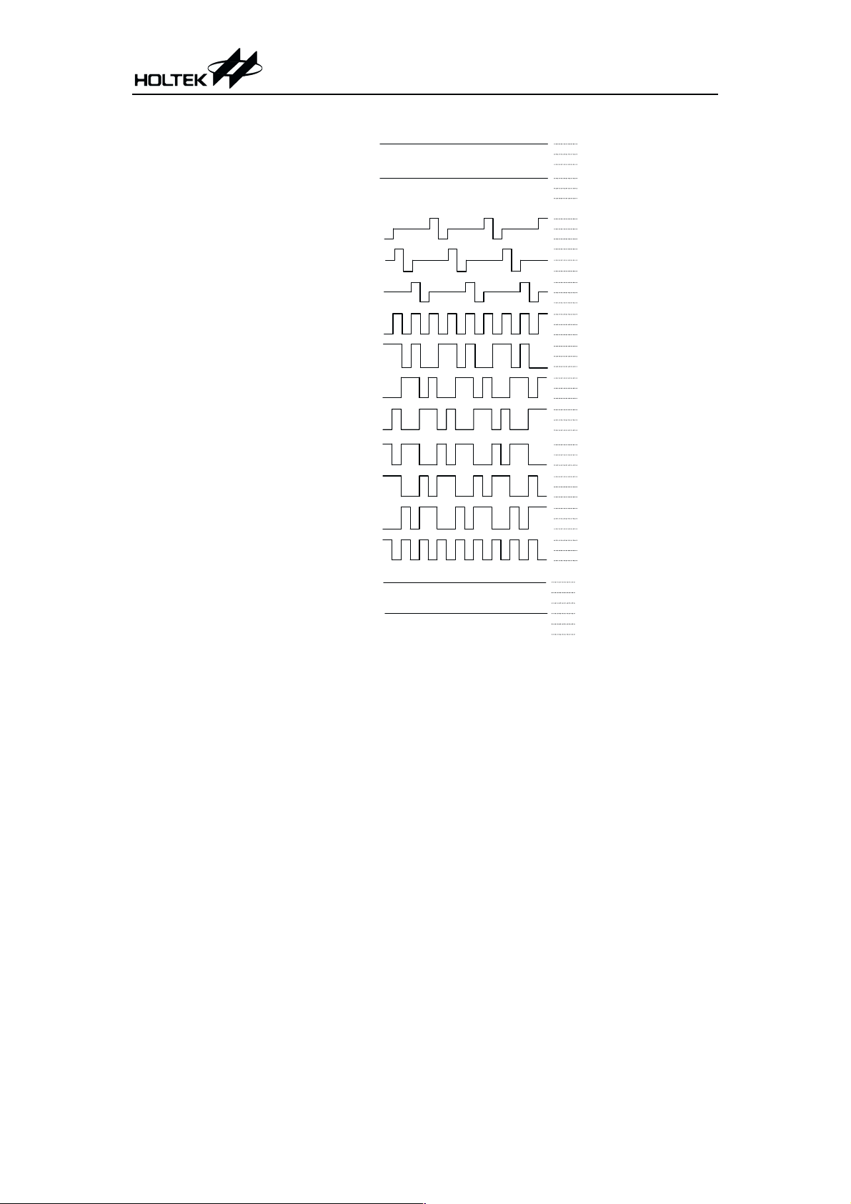
D uring a R eset P u lse:
COM 0,COM 1,COM 2
All LCD driver outputs
Norm al O peration M ode :
COM 0
COM 1
COM 2
LC D segm ents on C O M
0,1,2 sides being unlit
O nly LC D segm ents on
C O M 0 side being lit
O nly LC D segm ents on
C O M 1 side being lit
O nly LC D segm ents on
C O M 2 side being lit
LC D segm ents on
C O M 0,1 sides being lit
LC D segm ents on
C O M 0,2 sides being lit
LC D segm ents on
C O M 1,2 sides being lit
LC D segm ents on
C O M 0,1,2 sides being lit
Halt Mode:
COM 0,COM 1,COM 2
All LCD driver outputs
VDD
1/2 VD D
VSS
VDD
1/2 VD D
VSS
VDD
1/2 VD D
VSS
VDD
1/2 VD D
VSS
VDD
1/2 VD D
VSS
VDD
1/2 VD D
VSS
VDD
1/2 VD D
VSS
VDD
1/2 VD D
VSS
VDD
1/2 VD D
VSS
VDD
1/2 VD D
VSS
VDD
1/2 VD D
VSS
VDD
1/2 VD D
VSS
VDD
1/2 VD D
VSS
VDD
1/2 VD D
VSS
VDD
1/2 VD D
VSS
LCD driver output (1/3 duty, 1/2 bias)
31 January 18, 2000
Page 32

3/2VD D
VDD
HT47C20
COM 0
COM 1
COM 2
COM 3
LC D segm ents O N
C O M 2 side lighted
1/2 V D D
VSS
3/2VD D
VDD
1/2 V D D
VSS
3/2VD D
VDD
1/2 V D D
VSS
3/2VD D
VDD
1/2 V D D
VSS
3/2VD D
VDD
1/2 V D D
VSS
LCD driver output (1/4 duty, 1/3 bias)
32 January 18, 2000
Page 33

HT47C20
Buzzer
HT47C20 provides a pair of buzzer output BZ and
BZ
, which share pins with PA0 and PA1 respec
tively, as determined by mask option. Its output
frequency can also be selected by mask option.
When the buzzer function is selected, setting
PA.0 and PA.1 ²0² simultaneously will enable
the buzzer output and setting PA.0 ²1² will dis
able the buzzer output and setting PA.0 ²0² and
PA.1 ²1² will only enable the BZ output and dis
able the BZ
(CLR PA.1)0(CLR PA.0)
(SET PA.1)0(CLR PA.0)
IR carrier
HT47C20 provides carrier driving capability
that allows for easy interfacing to an infrared
diode, which share pin with PA2, as determined
by mask option.
output.
PA1 PA0 Function
0
1
X
1
(SET PA.0)
Buzzer enable
PA0=BZ,
PA1=BZ
PA0=BZ,
PA1=0
PA0=0,
PA1=0
When the carrier option is selected, setting PA2
²0² (²CLR PA.2²) will enable the carrier output
and setting PA2 ²1² (²SET PA.2²) will disable
the carrier output and the PA2 output is at low
level. The IR carrier frequency is system clock
divided by 12 and it is 1/4 duty.
PA2 Function
-
-
0
(CLR PA.2)
1
(SET PA.2)
Programmable frequency divider ¾ PFD
The PFD output shares pin with PA3, as deter
mined by mask option.
When the PFD option is selected, setting PA3
²0² (²CLR PA.3²) will enable the PFD output
and setting PA3 ²1² (²SET PA.3²) will disable
the PFD output and PA3 output at low level.
PFD output frequency =
1
´
2
timer overflow period
0 (CLR PA.2) PA3= PFD output
1 (SET PA.2) PA3= 0
PA2=IR carrier output
PA2=0
1
PA3 Function
-
Register Bit No. Label Read/Write Reset Function
RTCC
(09H)
0
1
2
3
4 SAVE R/W 0
5
6, 7
RT0
RT1
RT2
¾¾¾Unused bit, this bit must clear to ²0²
¾¾¾
¾¾¾Unused bits, read as ²0²
R/W
1
8 to 1 multiplexer control inputs to select the
1
real time clock prescaler output
1
Control the RTC OSC to oscillate quickly.
²0² enable
²1² disable
After power on, set this bit to ²1² to reduce
power comsumption
Unused bit, this bit is unknow for reading
RTCC Register
33 January 18, 2000
Page 34

HT47C20
Mask option
The following shows many kinds of mask options in the HT47C20. All these options should be defined
in order to ensure proper system functioning.
No. Mask Option
OSC type selection. This option is to decide if an RC or a crystal oscillator is chosen as sys
1
tem clock.
Clock source selection of WDT, RTC and Time Base. There are three types of selection: sys
2
tem clock/4 or RTC OSC or WDT OSC.
3 WDT enable/disable selection. WDT can be enabled or disabled by mask option.
CLR WDT times selection. This option defines how to clear the WDT by instruction. One
4
time means that the ²CLR WDT² can clear the WDT. ²Two times² means that only if both
of the ²CLR WDT1² and ²CLR WDT2² have been executed, then WDT can be cleared.
Time Base time-out period selection. The Time Base time-out period ranges from f
5
/215. ²fs² means the clock source selected by mask option.
f
s
Buzzer output frequency selection. There are eight types frequency signals for buzzer out
6
put: f
s
Wake-up selection. This option defines the wake-up function activity. External I/O pins
7
(PA only) all have the capability to wake-up the chip from a halt mode by a following edge.
Pull high selection. This option is to decide whether the pull high resistance is viable or not
8
on the low nibble of the PA.
/22~f
9
. ²fs² means the clock source selected by mask option.
s/2
PA CMOS or NMOS selection.
The structure of the low nibble of the PA can be selected to be CMOS or NMOS. When the
9
CMOS is selected, the related pins only can be used for output operations. When the NMOS
is selected, the related pins can be used for input or output operations.
I/O pins share with other function selection.
PA0/BZ, PA1/BZ
10
PA2/IR: PA2 can be set as I/O pins or IR carrier output.
: PA0 and PA1 can be set as I/O pins or buzzer outputs.
PA3/PFD: PA3 can be set as I/O pins or PFD output.
LCD common selection. There are two types of selection: 3 commons (1/3 duty, 1/2 bias) or 4
commons (1/4 duty, 1/3 bias). If the 4 commons is selected, the segment output pin
11
²SEG19/COM3² will be set as a common output ²COM3².
LCD driver clock selection. There are seven types of frequency signals for the LCD driver
12
circuits: f
LCD on or LCD off at the halt mode selection.
13
The LCD can be enable or disable at the halt mode by mask option.
/22~fs/28. ²fs² means the clock source selection by mask option.
s
/212to
s
-
-
-
34 January 18, 2000
Page 35

Application Circuits
HT47C20
R C o s c illa t o r a p p lic a tio n
(1 /3 b ia s )
OSC1
OSC2
V
DD
RES
HT47C20
OSC3
32768H z
OSC4
IN T
TM R
SEG0~18
COM 0~3
C1
C2
V1
V2
V3
IN 0
CS0
CRT0
RT0
RS0
IN 1
CS1
RS1
RT1
PA0~PA7
PB0~PB3
LC D
PANEL
V
DD
R or C
C r y s t a l o s c illa t o r a p p lic a tio n
(1 /3 b ia s )
OSC1
OSC2
V
DD
RES
HT47C20
OSC3
32768H z
OSC4
IN T
TM R
SEG0~18
COM 0~3
C1
C2
V1
V2
V3
IN 0
CS0
CRT0
RT0
RS0
IN 1
CS1
RS1
RT1
PA0~PA7
PB0~PB3
LC D
PANEL
V
DD
R or C
35 January 18, 2000
Page 36

HT47C20
R C o s c illa t o r a p p lic a tio n
(1 /2 b ia s )
OSC1
OSC2
V
DD
RES
HT47C20
OSC3
32768H z
OSC4
IN T
TM R
SEG0~19
COM 0~2
C1
C2
IN 0
CS0
CRT0
RT0
RS0
IN 1
CS1
RS1
RT1
PA0~PA7
PB0~PB3
V1
V2
V3
LC D
PANEL
V
DD
R or C
C r y s t a l o s c illa t o r a p p lic a tio n
(1 /2 b ia s )
OSC1
OSC2
V
DD
RES
HT47C20
OSC3
32768H z
OSC4
IN T
TM R
SEG0~19
COM 0~2
C1
C2
V1
V2
V3
IN 0
CS0
CRT0
RT0
RS0
IN 1
CS1
RS1
RT1
PA0~PA7
PB0~PB3
LC D
PANEL
V
DD
R or C
36 January 18, 2000
Page 37

HT47C20
Instruction Set Summary
Mnemonic Description Flag Affected
Arithmetic
ADD A,[m]
ADDM A,[m]
ADD A,x
ADC A,[m]
ADCM A,[m]
SUB A,x
SUB A,[m]
SUBM A,[m]
SBC A,[m]
SBCM A,[m]
DAA [m]
Logic Operation
AND A,[m]
OR A,[m]
XOR A,[m]
ANDM A,[m]
ORM A,[m]
XORM A,[m]
AND A,x
OR A,x
XOR A,x
CPL [m]
CPLA [m]
Increment & Decrement
INCA [m]
INC [m]
DECA [m]
DEC [m]
Rotate
RRA [m]
RR [m]
RRCA [m]
RRC [m]
RLA [m]
RL [m]
RLCA [m]
RLC [m]
Add data memory to ACC
Add ACC to data memory
Add immediate data to ACC
Add data memory to ACC with carry
Add ACC to register with carry
Subtract immediate data from ACC
Subtract data memory from ACC
Subtract data memory from ACC with result in data memory
Subtract data memory from ACC with carry
Subtract data memory from ACC with carry and result in
data memory
Decimal adjust ACC for addition with result in data memory
AND data memory to ACC
OR data memory to ACC
Exclusive-OR data memory to ACC
AND ACC to data memory
OR ACC to data memory
Exclusive-OR ACC to data memory
AND immediate data to ACC
OR immediate data to ACC
Exclusive-OR immediate data to ACC
Complement data memory
Complement data memory with result in ACC
Increment data memory with result in ACC
Increment data memory
Decrement data memory with result in ACC
Decrement data memory
Rotate data memory right with result in ACC
Rotate data memory right
Rotate data memory right through carry with result in ACC
Rotate data memory right through carry
Rotate data memory left with result in ACC
Rotate data memory left
Rotate data memory left through carry with result in ACC
Rotate data memory left through carry
Z, C, AC, OV
Z, C, AC, OV
Z, C, AC, OV
Z, C, AC, OV
Z, C, AC, OV
Z, C, AC, OV
Z, C, AC, OV
Z, C, AC, OV
Z, C, AC, OV
Z, C, AC, OV
None
None
None
None
C
Z
Z
Z
Z
Z
Z
Z
Z
Z
Z
Z
Z
Z
Z
Z
C
C
C
C
37 January 18, 2000
Page 38

HT47C20
Mnemonic Description Flag Affected
Data Move
MOV A,[m]
MOV [m],A
MOV A,x
Bit Operation
CLR [m].i
SET [m].i
Branch
JMP addr
SZ [m]
SZA [m]
SZ [m].i
SNZ [m].i
SIZ [m]
SDZ [m]
SIZA [m]
SDZA [m]
CALL addr
RET
RET A,x
RETI
Table Read
TABRDC [m]
TABRDL [m]
Miscellaneous
NOP
CLR [m]
SET [m]
CLR WDT
CLR WDT1
CLR WDT2
SWAP [m]
SWAPA [m]
HALT
Move data memory to ACC
Move ACC to data memory
Move immediate data to ACC
Clear bit of data memory
Set bit of data memory
Jump unconditional
Skip if data memory is zero
Skip if data memory is zero with data movement to ACC
Skip if bit i of data memory is zero
Skip if bit i of data memory is not zero
Skip if increment data memory is zero
Skip if decrement data memory is zero
Skip if increment data memory is zero with result in ACC
Skip if decrement data memory is zero with result in ACC
Subroutine call
Return from subroutine
Return from subroutine and load immediate data to ACC
Return from interrupt
Read ROM code (current page) to data memory and TBLH
Read ROM code (last page) to data memory and TBLH
No operation
Clear data memory
Set data memory
Clear watchdog timer
Pre-clear watchdog timer
Pre-clear watchdog timer
Swap nibbles of data memory
Swap nibbles of data memory with result in ACC
Enter power down mode
None
None
None
None
None
None
None
None
None
None
None
None
None
None
None
None
None
None
None
None
None
None
None
TO, PD
TO*, PD*
TO*, PD*
None
None
TO, PD
Note: x: 8 bits immediate data
m: 7 bits data memory address
A: accumulator
i: 0~7 number of bits
addr: 11 bits program memory address
Ö: Flag is affected
-: Flag is not affected
*: Flag may be affected by the execution status
38 January 18, 2000
Page 39

HT47C20
Instruction Definition
ADC A,[m] Add data memory and carry to accumulator
Description The contents of the specified data memory, accumulator and the carry
flag are added simultaneously, leaving the result in the accumulator.
Operation
Affected flag(s)
ADCM A,[m] Add accumulator and carry to data memory
Description The contents of the specified data memory, accumulator and the carry
Operation
Affected flag(s)
ACC ¬ ACC+[m]+C
TC2 TC1 TO PD OV Z AC C
¾¾¾¾ÖÖÖÖ
flag are added simultaneously, leaving the result in the specified data
memory.
[m] ¬ ACC+[m]+C
TC2 TC1 TO PD OV Z AC C
¾¾¾¾ÖÖÖÖ
ADD A,[m] Add data memory to accumulator
Description The contents of the specified data memory and the accumulator are
added. The result is stored in the accumulator.
Operation
Affected flag(s)
ADD A,x Add immediate data to accumulator
Description The contents of the accumulator and the specified data are added, leav
Operation
Affected flag(s)
ACC ¬ ACC+[m]
TC2 TC1 TO PD OV Z AC C
¾¾¾¾ÖÖÖÖ
ing the result in the accumulator.
ACC ¬ ACC+x
TC2 TC1 TO PD OV Z AC C
¾¾¾¾ÖÖÖÖ
39 January 18, 2000
-
Page 40

HT47C20
ADDM A,[m] Add accumulator to data memory
Description The contents of the specified data memory and the accumulator are
added. The result is stored in the data memory.
Operation
Affected flag(s)
AND A,[m] Logical AND accumulator with data memory
Description Data in the accumulator and the specified data memory performs a
Operation
Affected flag(s)
AND A,x Logical AND immediate data to accumulator
Description Data in the accumulator and the specified data performs a bitwise logi
Operation
Affected flag(s)
[m] ¬ ACC+[m]
TC2 TC1 TO PD OV Z AC C
¾¾¾¾ÖÖÖÖ
bitwise logical_AND operation. The result is stored in the accumulator.
ACC ¬ ACC ²AND² [m]
TC2 TC1 TO PD OV Z AC C
¾¾¾¾¾Ö¾¾
cal_AND operation. The result is stored in the accumulator.
ACC ¬ ACC ²AND² x
TC2 TC1 TO PD OV Z AC C
¾¾¾¾¾Ö¾¾
-
ANDM A,[m] Logical AND data memory with accumulator
Description Data in the specified data memory and the accumulator performs a
bitwise logical_AND operation. The result is stored in the data memory.
Operation
Affected flag(s)
[m] ¬ ACC ²AND² [m]
TC2 TC1 TO PD OV Z AC C
¾¾¾¾¾Ö¾¾
40 January 18, 2000
Page 41

HT47C20
CALL addr Subroutine call
Description The instruction unconditionally calls a subroutine located at the indi
cated address. The program counter increments once to obtain the ad
dress of the next instruction, and pushes this onto the stack. The
indicated address is then loaded. Program execution continues with the
instruction at this address.
Operation
Affected flag(s)
CLR [m] Clear data memory
Description The contents of the specified data memory are cleared to zero.
Operation
Affected flag(s)
CLR [m].i Clear bit of data memory
Description The bit i of the specified data memory is cleared to zero.
Operation
Affected flag(s)
Stack ¬ PC+1
PC ¬ addr
TC2 TC1 TO PD OV Z AC C
¾¾¾¾¾¾¾¾
[m] ¬ 00H
TC2 TC1 TO PD OV Z AC C
¾¾¾¾¾¾¾¾
[m].i ¬ 0
TC2 TC1 TO PD OV Z AC C
¾¾¾¾¾¾¾¾
-
-
CLR WDT Clear watchdog timer
Description The WDT is cleared. The power down bit (PD) and time-out bit (TO) are
cleared.
Operation
Affected flag(s)
WDT last two bits ¬ 00H
PD&TO¬ 0
TC2 TC1 TO PD OV Z AC C
¾¾
00
¾¾¾¾
41 January 18, 2000
Page 42

HT47C20
CLR WDT1 Preclear watchdog timer
Description The PD, TO flags and WDT are cleared, if the other preclear WDT in
struction had been executed. Only execution of this instruction without
the other preclear instruction sets the indicating flag which implies that
this instruction was executed and the PD and TO flags remain un
changed.
Operation
Affected flag(s)
CLR WDT2 Preclear watchdog timer
Description The PD, TO flags and WDT are cleared, if the other preclear WDT in
Operation
Affected flag(s)
WDT last two bits ¬ 00H*
PD and TO ¬ 0*
TC2 TC1 TO PD OV Z AC C
¾¾
struction had been executed. Only execution of this instruction without
the other preclear instruction sets the indicating flag which implies that
this instruction was executed and the PD and TO flags remain un
changed.
WDT last two bits ¬ 00H*
PD and TO ¬ 0*
TC2 TC1 TO PD OV Z AC C
¾¾
0* 0*
0* 0*
¾¾¾¾
¾¾¾¾
-
-
-
-
CPL [m] Complement data memory
Description Each bit of the specified data memory is logically complemented (1 s
complement). Bits which previously contain a one are changed to zero
and vice-versa.
Operation
Affected flag(s)
[m]¬ [m
TC2 TC1 TO PD OV Z AC C
]
¾¾¾¾¾Ö¾¾
42 January 18, 2000
Page 43

HT47C20
CPLA [m] Complement data memory-place result in accumulator
Description Each bit of the specified data memory is logically complemented (1 s
complement). Bits which previously contained a one are changed to zero
and vice-versa. The complemented result is stored in the accumulator
and the contents of the data memory remains unchanged.
Operation
Affected flag(s)
DAA [m] Decimal-Adjust accumulator for addition
Description The accumulator value is adjusted to the BCD(Binary Code Decimal)
Operation If (ACC.3~ACC.0) >9 or AC=1
Affected flag(s)
ACC ¬ [m
TC2 TC1 TO PD OV Z AC C
¾¾¾¾¾Ö¾¾
code. The accumulator is divided into two nibbles. Each nibble is ad
justed to the BCD code and an internal carry (AC1) will be done if the low
nibble of the accumulator is greater than 9. The BCD adjustment is done
by adding 6 to the original value if the original value is greater than 9 or
a carry (AC or C) is set; otherwise the original value remains unchanged.
The result is stored in the data memory and only the carry flag (C) may
be affected.
then ([m].3~[m].0) ¬ (ACC.3~ACC.0)+6, AC1=AC
else ([m].3~[m].0) ¬ (ACC.3~ACC.0), AC1=0
If (ACC.7~ACC.4)+AC1 >9 or C=1
then ([m].7~[m].4) ¬ (ACC.7~ACC.4)+6+AC1, C=1
else ([m].7~[m].4) ¬ (ACC.7~ACC.4)+AC1, C=C
TC2 TC1 TO PD OV Z AC C
¾¾¾¾¾¾¾ Ö
]
-
DEC [m] Decrement data memory
Description Data in the specified data memory is decremented by one.
Operation
Affected flag(s)
[m] ¬ [m]-1
TC2 TC1 TO PD OV Z AC C
¾¾¾¾¾Ö¾¾
43 January 18, 2000
Page 44

HT47C20
DECA [m] Decrement data memory-place result in accumulator
Description Data in the specified data memory is decremented by one, leaving the re
sult in the accumulator. The contents of the data memory remain un
changed.
Operation
Affected flag(s)
HALT Enter power down mode
Description This instruction stops program execution and turns off the system clock.
Operation
Affected flag(s)
ACC ¬ [m]-1
TC2 TC1 TO PD OV Z AC C
¾¾¾¾¾Ö¾¾
The contents of the RAM and registers are retained. The WDT is cleared.
The power down bit (PD) is set and the WDT time-out bit (TO) is cleared.
PC ¬ PC+1
PD ¬ 1
TO ¬ 0
TC2 TC1 TO PD OV Z AC C
¾¾
01
¾¾¾¾
-
-
INC [m] Increment data memory
Description Data in the specified data memory is incremented by one.
Operation
Affected flag(s)
INCA [m] Increment data memory and place result in accumulator
Description Data in the specified data memory is incremented by one, leaving the re-
Operation
Affected flag(s)
[m] ¬ [m]+1
TC2 TC1 TO PD OV Z AC C
¾¾¾¾¾Ö¾¾
sult in the accumulator. The contents of the data memory remain un
changed.
ACC ¬ [m]+1
TC2 TC1 TO PD OV Z AC C
¾¾¾¾¾Ö¾¾
44 January 18, 2000
-
Page 45

HT47C20
JMP addr Direct Jump
Description Bits 0~10 of the program counter are replaced with the directly-specified
address unconditionally, and control passed to this destination.
Operation
Affected flag(s)
MOV A,[m] Move data memory to accumulator
Description The contents of the specified data memory is copied to the accumulator.
Operation
Affected flag(s)
MOV A,x Move immediate data to accumulator
Description The 8 bit data specified by the code is loaded into the accumulator .
Operation
Affected flag(s)
PC ¬ addr
TC2 TC1 TO PD OV Z AC C
¾¾¾¾¾¾¾¾
ACC ¬ [m]
TC2 TC1 TO PD OV Z AC C
¾¾¾¾¾¾¾¾
ACC ¬ x
TC2 TC1 TO PD OV Z AC C
¾¾¾¾¾¾¾¾
MOV [m],A Move accumulator to data memory
Description The contents of the accumulator is copied to the specified data memory
(one of the data memories).
Operation
Affected flag(s)
NOP No operation
Description No operation is performed. Execution continues with the next instruc
Operation
Affected flag(s)
[m] ¬ ACC
TC2 TC1 TO PD OV Z AC C
¾¾¾¾¾¾¾¾
tion.
PC ¬ PC+1
TC2 TC1 TO PD OV Z AC C
¾¾¾¾¾¾¾¾
45 January 18, 2000
-
Page 46

HT47C20
OR A,[m] Logical OR accumulator with data memory
Description Data in the accumulator and the specified data memory (one of the data
memories) performs a bitwise logical_OR operation. The result is stored
in the accumulator.
Operation
Affected flag(s)
OR A,x Logical OR immediate data to accumulator
Description Data in the accumulator and the specified data performs a bitwise logi
Operation
Affected flag(s)
ORM A,[m] Logical OR data memory with accumulator
Description Data in the data memory (one of the data memories) and the accumula
Operation
Affected flag(s)
ACC ¬ ACC ²OR² [m]
TC2 TC1 TO PD OV Z AC C
¾¾¾¾¾Ö¾¾
cal_OR operation. The result is stored in the accumulator.
ACC ¬ ACC ²OR² x
TC2 TC1 TO PD OV Z AC C
¾¾¾¾¾Ö¾¾
tor performs a bitwise logical_OR operation. The result is stored in the
data memory.
[m] ¬ ACC ²OR² [m]
TC2 TC1 TO PD OV Z AC C
¾¾¾¾¾Ö¾¾
-
-
RET Return from subroutine
Description The program counter is restored from the stack. This is a two-cycle in-
struction.
Operation
Affected flag(s)
PC ¬ Stack
TC2 TC1 TO PD OV Z AC C
¾¾¾¾¾¾¾¾
46 January 18, 2000
Page 47

HT47C20
RET A,x Return and place immediate data in accumulator
Description The program counter is restored from the stack and the accumulator
loaded with the specified 8-bit immediate data.
Operation
Affected flag(s)
RETI Return from interrupt
Description The program counter is restored from the stack, and interrupts enabled
Operation
Affected flag(s)
RL [m] Rotate data memory left
Description The contents of the specified data memory is rotated left one bit with bit
Operation
Affected flag(s)
PC ¬ Stack
ACC ¬ x
TC2 TC1 TO PD OV Z AC C
¾¾¾¾¾¾¾¾
by setting the EMI bit. EMI is the enable master (global) interrupt bit
(bit 0; register INTC).
PC ¬ Stack
EMI ¬ 1
TC2 TC1 TO PD OV Z AC C
¾¾¾¾¾¾¾¾
7 rotated into bit 0.
[m].(i+1) ¬ [m].i; [m].i:bit i of the data memory (i=0-6)
[m].0 ¬ [m].7
TC2 TC1 TO PD OV Z AC C
¾¾¾¾¾¾¾¾
RLA [m] Rotate data memory left and place result in accumulator
Description Data in the specified data memory is rotated left one bit with bit 7 ro
tated into bit 0, leaving the rotated result in the accumulator. The con
tents of the data memory remain unchanged.
Operation
Affected flag(s)
ACC.(i+1) ¬ [m].i; [m].i:bit i of the data memory (i=0-6)
ACC.0 ¬ [m].7
TC2 TC1 TO PD OV Z AC C
¾¾¾¾¾¾¾¾
47 January 18, 2000
-
-
Page 48

HT47C20
RLC [m] Rotate data memory left through carry
Description The contents of the specified data memory and the carry flag are together
rotated left one bit. Bit 7 replaces the carry bit; the original carry flag is
rotated into the bit 0 position.
Operation
Affected flag(s)
RLCA [m] Rotate left through carry and place result in accumulator
Description Data in the specified data memory and the carry flag are together ro
Operation
Affected flag(s)
[m].(i+1) ¬ [m].i; [m].i:bit i of the data memory (i=0-6)
[m].0 ¬ C
C ¬ [m].7
TC2 TC1 TO PD OV Z AC C
¾¾¾¾¾¾¾ Ö
tated left one bit. Bit 7 replaces the carry bit and the original carry flag is
rotated into bit 0 position. The rotated result is stored in the accumulator
but the contents of the data memory remain unchanged.
ACC.(i+1) ¬ [m].i; [m].i:bit i of the data memory (i=0-6)
ACC.0 ¬ C
C ¬ [m].7
TC2 TC1 TO PD OV Z AC C
¾¾¾¾¾¾¾ Ö
-
RR [m] Rotate data memory right
Description The contents of the specified data memory are rotated right one bit with
bit 0 rotated to bit 7.
Operation
Affected flag(s)
[m].i ¬ [m].(i+1); [m].i:bit i of the data memory (i=0-6)
[m].7 ¬ [m].0
TC2 TC1 TO PD OV Z AC C
¾¾¾¾¾¾¾¾
48 January 18, 2000
Page 49

HT47C20
RRA [m] Rotate right and place result in accumulator
Description Data in the specified data memory is rotated right one bit with bit 0 ro
tated into bit 7, leaving the rotated result in the accumulator. The con
tents of the data memory remain unchanged.
Operation
Affected flag(s)
RRC [m] Rotate data memory right through carry
Description The contents of the specified data memory and the carry flag are together
Operation
Affected flag(s)
ACC.(i) ¬ [m].(i+1); [m].i:bit i of the data memory (i=0-6)
ACC.7 ¬ [m].0
TC2 TC1 TO PD OV Z AC C
¾¾¾¾¾¾¾¾
rotated right one bit. Bit 0 replaces the carry bit; the original carry flag is
rotated into the bit 7 position.
[m].i ¬ [m].(i+1); [m].i:bit i of the data memory (i=0-6)
[m].7 ¬ C
C ¬ [m].0
TC2 TC1 TO PD OV Z AC C
¾¾¾¾¾¾¾ Ö
-
-
RRCA [m] Rotate right through carry and place result in accumulator
Description Data of the specified data memory and the carry flag are together rotated
right one bit. Bit 0 replaces the carry bit and the original carry flag is rotated into the bit 7 position. The rotated result is stored in the accumulator. The contents of the data memory remain unchanged.
Operation
Affected flag(s)
ACC.i ¬ [m].(i+1); [m].i:bit i of the data memory (i=0-6)
ACC.7 ¬ C
C ¬ [m].0
TC2 TC1 TO PD OV Z AC C
¾¾¾¾¾¾¾ Ö
49 January 18, 2000
Page 50

HT47C20
SBC A,[m] Subtract data memory and carry from accumulator
Description The contents of the specified data memory and the complement of the
carry flag are together subtracted from the accumulator, leaving the re
sult in the accumulator.
Operation
Affected flag(s)
SBCM A,[m] Subtract data memory and carry from accumulator
Description The contents of the specified data memory and the complement of the
Operation
Affected flag(s)
SDZ [m] Skip if decrement data memory is zero
Description The contents of the specified data memory are decremented by one. If the
Operation
Affected flag(s)
ACC ¬ ACC+[m
TC2 TC1 TO PD OV Z AC C
¾¾¾¾ÖÖÖÖ
carry flag are together subtracted from the accumulator, leaving the re
sult in the data memory.
[m] ¬ ACC+[m
TC2 TC1 TO PD OV Z AC C
¾¾¾¾ÖÖÖÖ
result is zero, the next instruction is skipped. If the result is zero, the fol
lowing instruction, fetched during the current instruction execution, is
discarded and a dummy cycle replaced to get the proper instruction. This
makes a 2-cycle instruction. Otherwise proceed with the next instruction.
Skip if ([m]-1)=0, [m] ¬ ([m]-1)
TC2 TC1 TO PD OV Z AC C
¾¾¾¾¾¾¾¾
]+C
]+C
-
-
-
50 January 18, 2000
Page 51

HT47C20
SDZA [m] Decrement data memory and place result in ACC, skip if zero
Description The contents of the specified data memory are decremented by one. If the
result is zero, the next instruction is skipped. The result is stored in the
accumulator but the data memory remains unchanged. If the result is
zero ,the following instruction, fetched during the current instruction ex
ecution, is discarded and a dummy cycle is replaced to get the proper in
struction, that makes a 2-cycle instruction. Otherwise proceed with the
next instruction.
Operation
Affected flag(s)
SET [m] Set data memory
Description Each bit of the specified data memory is set to one.
Operation
Affected flag(s)
Skip if ([m]-1)=0, ACC ¬ ([m]-1)
TC2 TC1 TO PD OV Z AC C
¾¾¾¾¾¾¾¾
[m] ¬ FFH
TC2 TC1 TO PD OV Z AC C
¾¾¾¾¾¾¾¾
-
-
SET [m].i Set bit of data memory
Description Bit i of the specified data memory is set to one.
Operation
Affected flag(s)
SIZ [m] Skip if increment data memory is zero
Description The contents of the specified data memory is incremented by one. If the
Operation
Affected flag(s)
[m].i ¬ 1
TC2 TC1 TO PD OV Z AC C
¾¾¾¾¾¾¾¾
result is zero, the following instruction, fetched during the current in
struction execution, is discarded and a dummy cycle is replaced to get the
proper instruction. This is a 2-cycle instruction. Otherwise proceed with
the next instruction.
Skip if ([m]+1)=0, [m] ¬ ([m]+1)
TC2 TC1 TO PD OV Z AC C
¾¾¾¾¾¾¾¾
51 January 18, 2000
-
Page 52

HT47C20
SIZA [m] Increment data memory and place result in ACC, skip if zero
Description The contents of the specified data memory is incremented by one. If the
result is zero, the next instruction is skipped and the result stored in the
accumulator. The data memory remains unchanged. If the result is zero,
the following instruction, fetched during the current instruction execu
tion, is discarded and a dummy cycle replaced to get the proper instruc
tion. This is a 2-cycle instruction. Otherwise proceed with the next
instruction.
Operation
Affected flag(s)
SNZ [m].i Skip if bit i of the data memory is not zero
Description If bit i of the specified data memory is not zero, the next instruction is
Operation
Affected flag(s)
Skip if ([m]+1)=0, ACC ¬ ([m]+1)
TC2 TC1 TO PD OV Z AC C
¾¾¾¾¾¾¾¾
skipped. If bit i of the data memory is not zero, the following instruction,
fetched during the current instruction execution, is discarded and a
dummy cycle is replaced to get the proper instruction. This is a 2-cycle in
struction. Otherwise proceed with the next instruction.
Skip if [m].i¹0
TC2 TC1 TO PD OV Z AC C
¾¾¾¾¾¾¾¾
-
-
-
SUB A,[m] Subtract data memory from accumulator
Description The specified data memory is subtracted from the contents of the accu-
mulator, leaving the result in the accumulator.
Operation
Affected flag(s)
SUBM A,[m] Subtract data memory from accumulator
Description The specified data memory is subtracted from the contents of the accu
Operation
Affected flag(s)
ACC ¬ ACC+[m
TC2 TC1 TO PD OV Z AC C
¾¾¾¾ÖÖÖÖ
mulator, leaving the result in the data memory.
[m] ¬ ACC [m
TC2 TC1 TO PD OV Z AC C
¾¾¾¾ÖÖÖÖ
]+1
]+1
52 January 18, 2000
-
Page 53

HT47C20
SUB A,x Subtract immediate data from accumulator
Description The immediate data specified by the code is subtracted from the contents
of the accumulator, leaving the result in the accumulator.
Operation
Affected flag(s)
SWAP [m] Swap nibbles within the data memory
Description The low-order and high-order nibbles of the specified data memory (one
Operation
Affected flag(s)
SWAPA [m] Swap data memory and place result in accumulator
Description The low-order and high-order nibbles of the specified data memory are
Operation
Affected flag(s)
ACC ¬ ACC+x
TC2 TC1 TO PD OV Z AC C
¾¾¾¾ÖÖÖÖ
of the data memories) are interchanged.
[m].3~[m].0 « [m].7~[m].4
TC2 TC1 TO PD OV Z AC C
¾¾¾¾¾¾¾¾
interchanged, writing the result to the accumulator. The contents of the
data memory remain unchanged.
ACC.3~ACC.0 ¬ [m].7~[m].4
ACC.7~ACC.4 ¬ [m].3~[m].0
TC2 TC1 TO PD OV Z AC C
¾¾¾¾¾¾¾¾
+1
SZ [m] Skip if data memory is zero
Description If the contents of the specified data memory is zero, the following instruc-
tion, fetched during the current instruction execution, is discarded and a
dummy cycle is replaced to get the proper instruction. This is a 2-cycle in
struction. Otherwise proceed with the next instruction.
Operation Skip if [m]=0
Affected flag(s)
TC2 TC1 TO PD OV Z AC C
¾¾¾¾¾¾¾¾
53 January 18, 2000
-
Page 54

HT47C20
SZA [m] Move data memory to ACC, skip if zero
Description The contents of the specified data memory is copied to accumulator. If the
contents is zero, the following instruction, fetched during the current in
struction execution, is discarded and a dummy cycle is replaced to get the
proper instruction. This is a 2-cycle instruction. Otherwise proceed with
the next instruction.
Operation
Affected flag(s)
SZ [m].i Skip if bit i of the data memory is zero
Description If bit i of the specified data memory is zero, the following instruction,
Operation Skip if [m].i=0
Affected flag(s)
Skip if [m]=0, ACC¬ [m]
TC2 TC1 TO PD OV Z AC C
¾¾¾¾¾¾¾¾
fetched during the current instruction execution, is discarded and a
dummy cycle is replaced to get the proper instruction. This is a 2-cycle in
struction. Otherwise proceed with the next instruction.
TC2 TC1 TO PD OV Z AC C
¾¾¾¾¾¾¾¾
-
-
TABRDC [m] Move the ROM code (current page) to TBLH and data memory
Description The low byte of ROM code (current page) addressed by the table pointer
(TBLP) is moved to the specified data memory and the high byte transferred to TBLH directly.
Operation
Affected flag(s)
[m] ¬ ROM code (low byte)
TBLH ¬ ROM code (high byte)
TC2 TC1 TO PD OV Z AC C
¾¾¾¾¾¾¾¾
54 January 18, 2000
Page 55

HT47C20
TABRDL [m] Move the ROM code (last page) to TBLH and data memory
Description The low byte of ROM code (last page) addressed by the table pointer
(TBLP) is moved to the data memory and the high byte transferred to
TBLH directly.
Operation
Affected flag(s)
XOR A,[m] Logical XOR accumulator with data memory
Description Data in the accumulator and the indicated data memory performs a
Operation
Affected flag(s)
XORM A,[m] Logical XOR data memory with accumulator
Description Data in the indicated data memory and the accumulator perform a
Operation
Affected flag(s)
[m] ¬ ROM code (low byte)
TBLH ¬ ROM code (high byte)
TC2 TC1 TO PD OV Z AC C
¾¾¾¾¾¾¾¾
bitwise logical Exclusive_OR operation and the result is stored in the ac
cumulator.
ACC ¬ ACC ²XOR² [m]
TC2 TC1 TO PD OV Z AC C
¾¾¾¾¾Ö¾¾
bitwise logical Exclusive_OR operation. The result is stored in the data
memory. The zero flag is affected.
[m] ¬ ACC ²XOR² [m]
TC2 TC1 TO PD OV Z AC C
¾¾¾¾¾Ö¾¾
-
XOR A,x Logical XOR immediate data to accumulator
Description Data in the accumulator and the specified data perform a bitwise logical
Exclusive_OR operation. The result is stored in the accumulator. The
zero flag is affected.
Operation
Affected flag(s)
ACC ¬ ACC ²XOR² x
TC2 TC1 TO PD OV Z AC C
¾¾¾¾¾Ö¾¾
55 January 18, 2000
Page 56

HT47C20
Holtek Semiconductor Inc. (Headquarters)
No.3 Creation Rd. II, Science-based Industrial Park, Hsinchu, Taiwan, R.O.C.
Tel: 886-3-563-1999
Fax: 886-3-563-1189
Holtek Semiconductor Inc. (Taipei Office)
5F, No.576, Sec.7 Chung Hsiao E. Rd., Taipei, Taiwan, R.O.C.
Tel: 886-2-2782-9635
Fax: 886-2-2782-9636
Fax: 886-2-2782-7128 (International sales hotline)
Holtek Semiconductor (Hong Kong) Ltd.
RM.711, Tower 2, Cheung Sha Wan Plaza, 833 Cheung Sha Wan Rd., Kowloon, Hong Kong
Tel: 852-2-745-8288
Fax: 852-2-742-8657
Copyright ã 2000 by HOLTEK SEMICONDUCTOR INC.
The information appearing in this Data Sheet is believed to be accurate at the time of publication. However, Holtek
assumes no responsibility arising from the use of the specifications described. The applications mentioned herein are
used solely for the purpose of illustration and Holtek makes no warranty or representation that such applications
will be suitable without further modification, nor recommends the use of its products for application that may pres
ent a risk to human life due to malfunction or otherwise. Holtek reserves the right to alter its products without prior
notification. For the most up-to-date information, please visit our web site at http://www.holtek.com.tw.
56 January 18, 2000
-
 Loading...