OTP CMOS 256K×8-Bit EPROM
Features
•
Operating voltage: +3.3V
•
Programming voltage
–
VPP=12.5V±0.2V
–
VCC=6.0V±0.2V
•
High-reliability CMOS technology
•
Latch-up immunity to 100mA from -1.0V to
V
+1.0V
CC
•
CMOS and TTL compatible I/O
•
Low power consumption
–
Active: 15mA max.
–
Standby: 1µA typ.
•
256K×8-bit organization
General Description
The HT27LC020 chip family is a low-power,
2048K (2,097,152) bit, +3.3V electrically onetime programmable (OTP ) rea d-only me morie s
(EPROM). Organized into 256K words with 8
bits per word, it features a fast singl e address
location programming, typically at 75
byte. Any byte can be accessed in less than
µs per
HT27LC020
•
Fast read access time: -120ns
•
Fast programming algorithm
•
Programming time 75µs typ.
•
Commercial and industrial temperature range
•
Two line controls (OE and CE)
•
Standard product identification code
•
Package type
–
32-pin DIP/SOP
–
32-pin PLCC
•
Commercial temperature ranges
(0
°C to +70°C)
120ns with respect to Spec. This eliminates the
need for WAIT states in high-performance microprocessor systems. The HT27LC020 has
separate Output Enable (
(
CE) controls which eliminate bus contention
issues.
OE) and Chip Enable
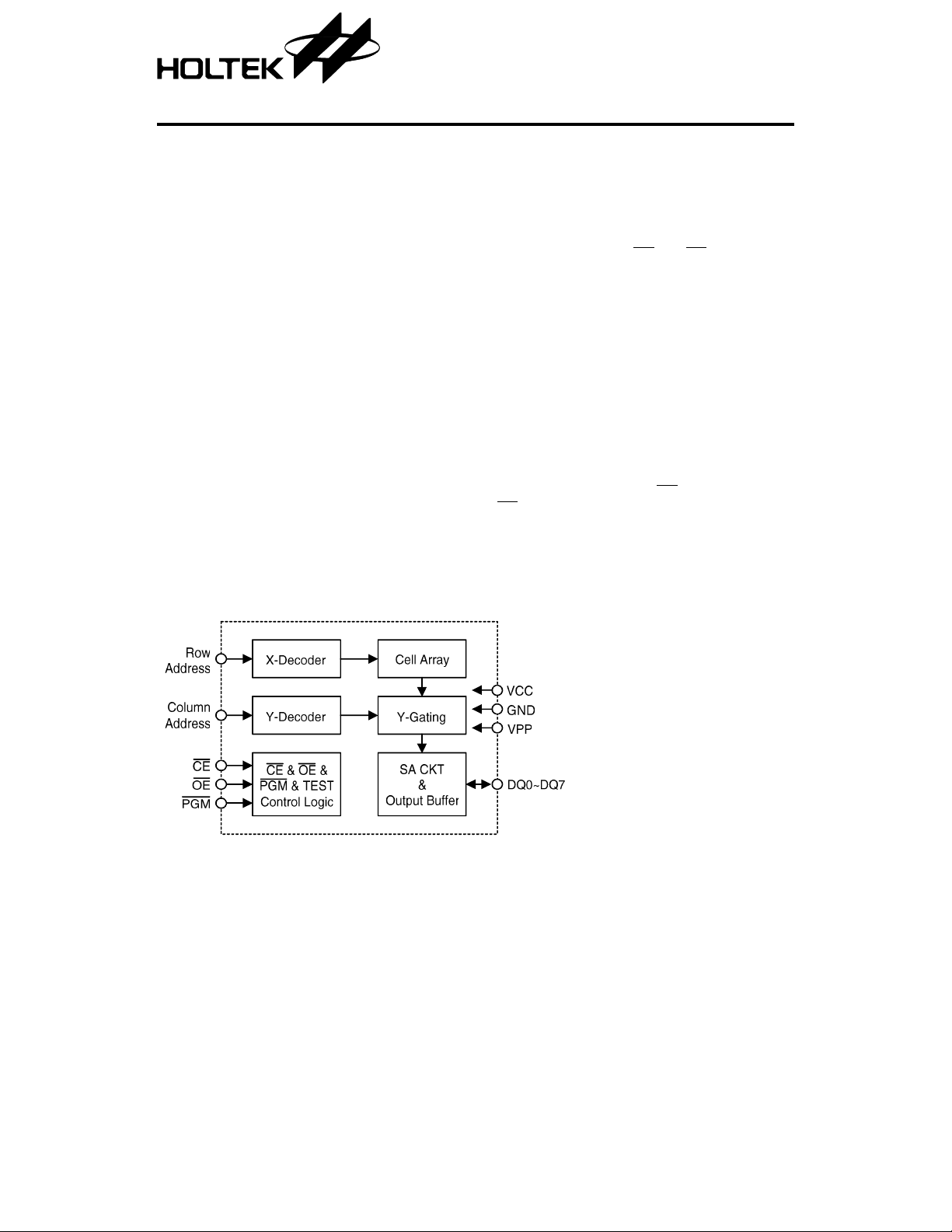
Block Diagram
1 7th May ’99

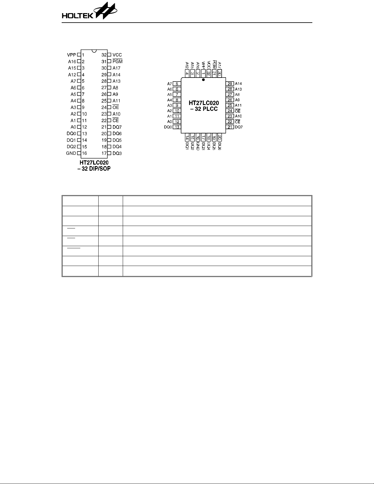
Pin Assignment
Pin Description
HT27LC020
Pin Name I/O/C/P Description
A0~A17 I Address input s
DQ0~DQ7 I/O Data inputs/outputs
CE C Chip enable
OE C Output enable
PGM C Program strobe
NC — No connection
VPP P Program voltage supply
2 7th May ’99

HT27LC020
Absolu te Maximum Ra tin g
Operation Temperature Commercial ...................................................................................0°C to +70°C
Storage Temperature.................................... .... .... .... .... .... .... .... .... .... .... .... .... .... .... .... .... .... .–65
Applied VCC Voltage with Respect to GND.................... .. .. .................... .. .. .................... .. . –0.6V to 7.0V
Applied Voltage on Input Pin with Respect to GND ......................................................... –0.6V to 7.0V
Applied Voltage on Output Pin with Respect to GND ............................. .. .. .. .. .. .. .. .. –0.6V to V
Applied Voltage on A9 Pin with Respect to GND..................................................... ...... . –0.6V to 13.5V
Applied VPP Voltage with Respect to GND............................................................ .... .... ..–0.6V to 13.5V
Applied READ V o ltage (Functionality is guaranteed between these limits) .................+3.0V to +3.6V
Note: These are stress ratings only. Stresses exceeding the range specified under “Absolute M axi-
mum Ratings” may cause substantial damage to the device. Functional operation of this device
at other conditions beyond those listed in the specification is not implied and prolonged
exposure to extreme condition s may affect device reliability.
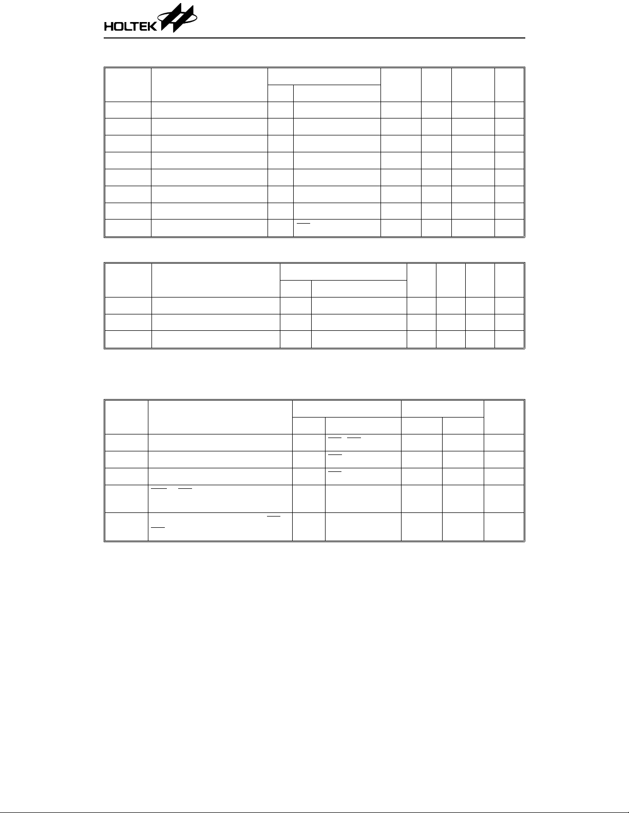
D.C. Characteristics
Read operation
Symbol Parameter
V
V
V
V
I
LI
I
LO
I
CC
I
SB1
I
SB2
I
PP
Output High Level 3.3V IOH=–0.4mA 2.4 — — V
OH
Output Low Level 3.3V IOL=2.0mA — — 0.45 V
OL
Input High Level 3.3V — 2.0 — VCC+0.5 V
IH
Input Low Level 3.3V — –0.3 — 0.8 V
IL
Input Leakage Current 3.3V VIN=0 to 3.6V –5 — 5 µA
Output Leakage Current 3.3V V
VCC Active Current 3.3V
Standby Current (CMOS) 3.3V CE=V
Standby Current (TTL) 3.3V CE=V
VPP Read/Standby Current 3.3V CE=OE=VIL, VPP=V
Test Conditions
V
CC
OUT
CE=VIL, f=5MHz,
I
OUT
Conditions
Min. Typ. Max. Unit
=0 to 3.6V –10 — 10 µA
=0mA
±0.3V — — 10 µA
CC
IH
—— 15 mA
— — 0.6 mA
—— 100 µA
CC
°C to 125°C
+0.5V
CC
3 7th May ’99

Programming operation
Symbol Parameter
V
OH
V
OL
V
IH
V
IL
I
LI
V
H
I
CC
I
PP
Output High Level 6V IOH=–0.4mA 2.4 — — V
Output Low Level 6V IOL=2.0mA — — 0.45 V
Input High Level 6V — 0.7V
Input Low Level 6V — –0.5 — 0.8 V
Input Load Current 6V VIN=VIL, V
A9 Product ID Voltage 6V — 11.5 — 12.5 V
VCC Supply Current 6V — — — 40 mA
VPP Supply Current 6V CE=V
Capacitance
Symbol Parameter
C
C
C
IN
OUT
VPP
Input Capacitance 3.3V VIN=0V — 8 12 pF
Output Capacitance 3.3V V
VPP Capacitance 3.3V VPP=0V — 18 25 pF
Test Conditions
V
CC
Conditions
Test Conditions
V
CC
HT27LC020
Min. T yp. Max. Unit
—VCC+0.5 V
CC
IH
IL
Conditions
=0V — 8 12 pF
OUT
— — 5.0 µA
——10mA
Min. Typ. Max. Unit
A.C. Characteristics
Read operation
Symbol Parameter
t
ACC
t
CE
t
OE
t
DF
t
OH
Address to Output Delay 3.3V CE=OE=V
Chip Enable to Output Delay 3.3V OE=V
Output Enable to Outpu t Delay 3.3V CE=V
CE or OE High to Output Float,
Whichever Occurred First
Output Hold from Address, CE or
OE, Whichever Occurred First
Test Conditions –120
V
CC
Conditions Min. Max.
IL
IL
IL
—120ns
—120ns
—45ns
Unit
3.3V — — 40 ns
3.3V — 0 — ns
4 7th May ’99
 Loading...