Features
•
Operating voltage: 2.7V ~5.5V
•
Low power consumption
–
Operation: 25mA Max. (VCC=5V)
10mA Max. (V
–
Standby: 30µA Max. (VCC=5V)
10
•
Access time:150ns Max. (VCC=5V)
µA Max. (V
250ns Max. (V
CC
CC
=3V)
CC
=3V)
=3V)
General Description
The HT23C128 is a read-only memory with
high performance CMOS storage device whose
128K of memory is arrange d into 16384 wo rds
by 8 bits.
For applica tion flexibility, the chip enable and
output enabl e control pins can be selected a s
active high or active low. This flexibility not
only allows easy interface with most microproc-
HT23C128
CMOS 16K×8-Bit Mask ROM
•
16384×8 bits of mask ROM
•
Mask options: chip enable CE/CE/OE2/OE 2
and output enable OE/
OE1/NC
•
TTL compatible inputs and outputs
•
Tristate outputs
•
Fully static operation
•
Package type: 28-pin DIP/SOP
essors, but also eliminates bus contention in
multiple bus mi cropro cessor syste ms. An add itional feature of the HT23C128 is its ability to
enter the standb y mode wh enever the chip enable (CE/
CE) is inactive, thus reducing current
consumption to below 30
these functions makes the chip suitable for high
density low power memory applications.
OE/NC & OE1/
µA. The combination of
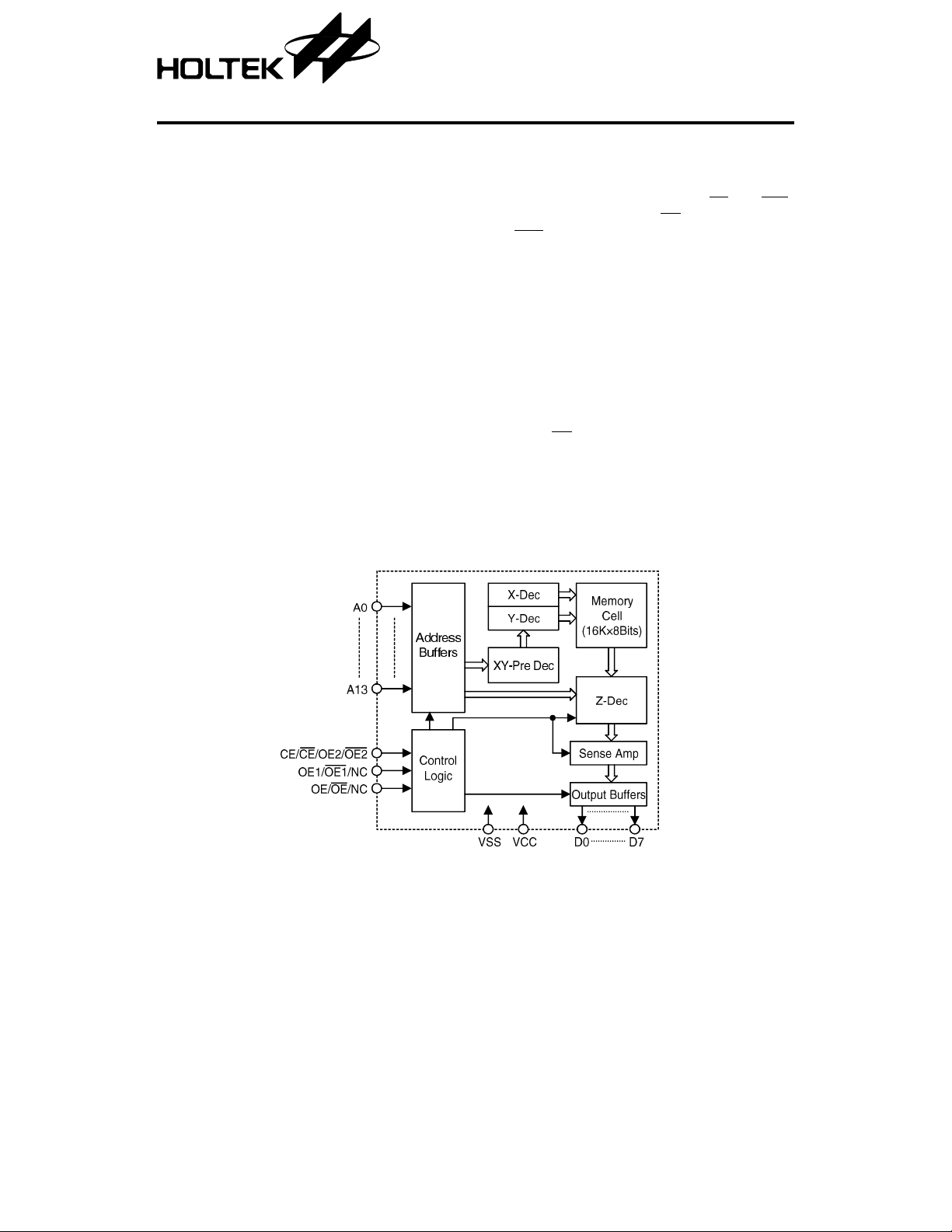
Block Diagram
1 24th Aug ’98

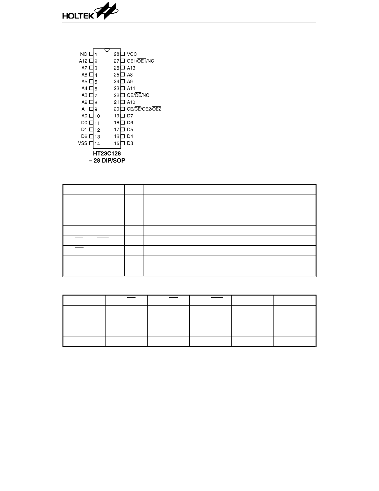
Pin Assignment
Pin Description
Pin Name I/O Description
NC — No connection
A0~A13 I Address inputs
D0~D7 O Data outputs
VSS I Negative power supply
CE/
CE/OE2/OE2 I Chip enable/Output enable input
OE/
OE/NC I Output enable input
OE1/
OE1/NC I Output enable input
VCC I Positive power supply
HT23C128
Operation Truth Table
Mode CE/CE OE/OE OE1/OE1 A0~A13 D0~D7
Read H/L H/L H/L Valid Data Out
Deselect H/L L/H X X High Z
Deselect H/L X L/H X High Z
Standby L/H X X X High Z
Note: H=V
, L=VIL, X=VIH or V
IH
IL
2 24th Aug ’98

HT23C128
Absolu te Maxim um Ratings *
Supply Voltage.................................–0.3V to 6V Storage Temperature.................–50°C to 125°C
Input Voltage........................–0.3V to V
*Note: These are stress ra tings on ly. Stresses exceeding the range specified under “Abso lute Maxi -
mum Ratings” ma y cause substantial damage to the device. Functional operation of this
device at other conditions beyond those listed in the specification is not implied and prolonged
exposure to extreme condition s may affect device reliability.
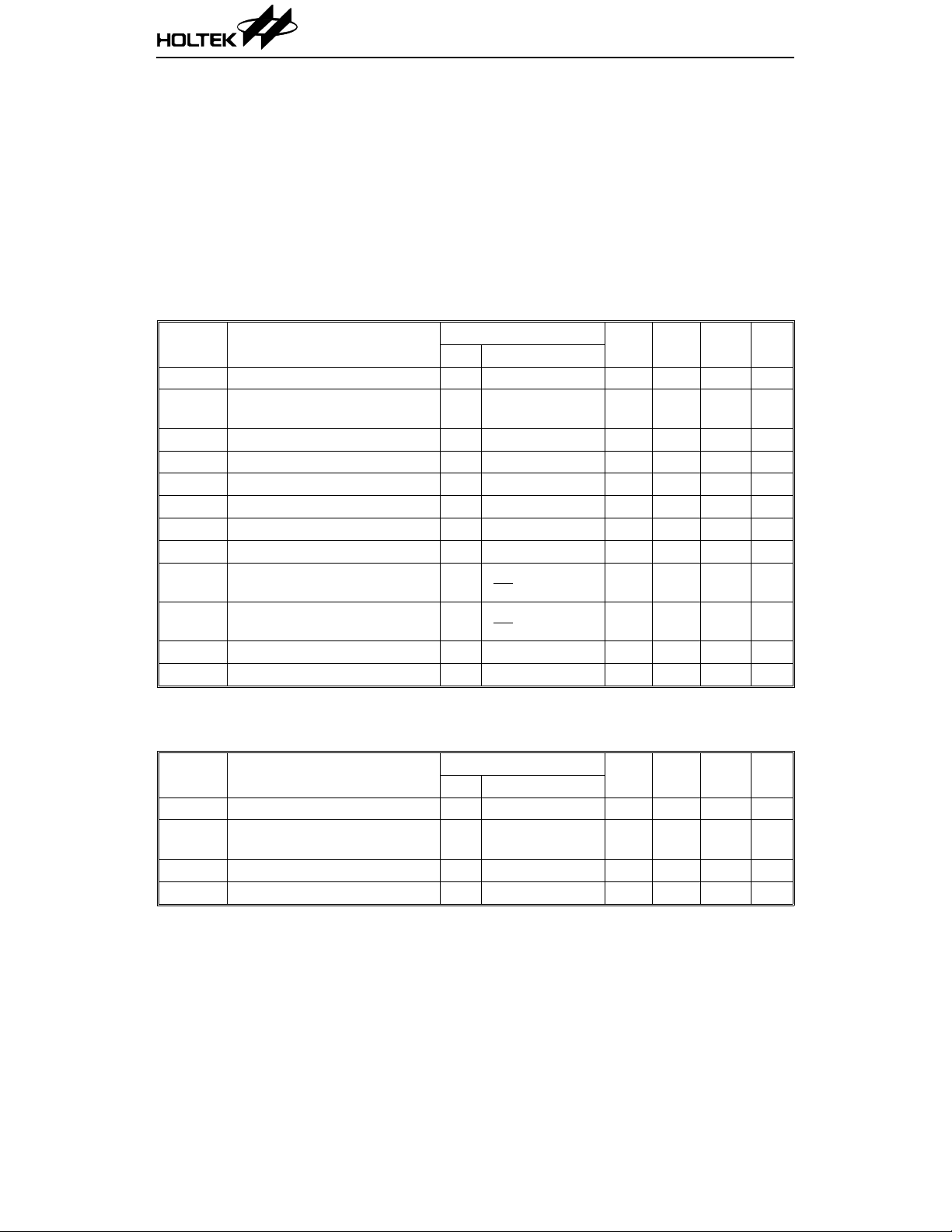
D.C. Characteristics
Supply voltage: 2.7V~3.6V Ta=–40°C to 85°C
+0.3V Operating Temperature...............–40°C to 85°C
CC
Symbol Parameter
V
CC
I
CC
V
IL
V
IH
V
OL
V
OH
I
LI
I
LO
I
STB1
I
STB2
C
IN
C
OUT
Operating Voltage — — 2.7 — 3.6 V
Operating Current 3V
Input Low Voltage 3 V — V
Input High Voltage 3V — 2.0 — V
Output Low Voltage 3V IOL=2.1mA — — 0.4 V
Output High Voltage 3V IOH=–0.4mA 2.4 — V
Input Leakage Current 3V VIN=0 to V
Output Leakage Current 3V V
Standby Current 3V
Standby Current 3V
Input Capacitance (See note) — f=1MHz — — 10 pF
Output Capacitance (See note) — f=1MHz — — 10 pF
Test Conditions
V
CC
Conditions
O/P Unload,
f=5MHz
OUT
CE=V
CE=V
≤0.2V
CE
CE≥VCC-0.2V
=0 to V
IL
IH
CC
Min. Typ. Max. Unit
——10mA
— 0.4 V
SS
——10µA
CC
——10µA
——500µA
——10
CC
CC
V
V
µA
Note: These parameters are periodically sampled but not 100% tested.
Supply voltage: 4.5V~5.5V Ta=–40°C to 85°C
Symbol Parameter
V
CC
I
CC
V
IL
V
IH
Operating Voltage — — 4.5 — 5.5 V
Operating Current 5V
Input Low Voltage 5 V — V
Input High Voltage 5V — 2.2 — V
Test Conditions
V
CC
Conditions
O/P Unload,
f=5MHz
Min. Typ. Max. Unit
——25mA
— 0.8 V
SS
V
CC
3 24th Aug ’98
 Loading...