

128´32 LCD Controller for I/O MCU
Technical Document
·
FAQs
·
Application Note
Features
·
Operating voltage: 2.7V~5.2V
·
Built-in 32kHz RC oscillator
·
External 32.768kHz crystal oscillator or 32kHz fre
quency source input
·
Standby current: <1mA at 3V, <2mAat5V
·
Internal resistor type: 1/6 bias or 1/5 bias, 1/32 duty,
and 1/16 duty
·
Three selectable LCD frame frequencies: 64Hz,
89Hz or 170Hz
·
Max. 128´32 patterns, 128 segments and 32 com
mons
·
144 segments and 16 commons selectable by com
mand method
·
Built-in bit-map display RAM: 4096 bits (=128´32 bits)
·
Built-in internal resistor type bias generator
HT1670
·
Six-wire interface (four data wires)
·
Eight kinds of time base/WDT selection
·
-
-
-
Time base or WDT overflow output
·
R/W address auto increment
·
Built-in buzzer driver (2kHz/4kHz)
·
Power down command reduces power consumption
·
Software configuration feature
·
Data mode and Command mode instructions
·
Three data accessing modes
·
Provides VLCD pin to adjust LCD operating voltage
and max. VLCD voltage up to 7V
·
Provides three kinds of bias current programming
·
Control of TN-type and STN-type LCDs
·
208-pin QFP package
Applications
·
Leisure products
·
Games
·
Personal digital assistant
General Description
HT1670 is a peripheral device specially designed for I/O
type MCU used to expand the display capability. The
max. display segment of the device are 4096 patterns
(128 segments and 32 commons). It also supports four
data bits interface, buzzer sound, Watchdog Timer or
time base timer functions. The HT1670 is a memory
mapping and multi-function LCD controller. Since the
·
Cellular phone
·
Global positioning system
·
Consumer electronics
HT1670 can control TN-type (Twisted Nematic) or
STN-type (Super Twisted Nematic) LCDs. The software
configuration feature of the HT1670 make it suitable for
multiple LCD applications including LCD modules and
display subsystems. Only six lines (CS
,WR, DB0~DB3)
are required for the interface between the host controller
and the HT1670.
Rev. 1.20 1 November 10, 2005

Block Diagram
HT1670
Pin Assignment
C O M 2 4
C O M 2 3
2 0 8
2 0 7 2 0 6 2 0 5 2 0 4 2 0 3 2 0 2 2 0 1 2 0 0 1 9 9 1 9 8 1 9 7 1 9 6 1 9 5 1 9 4 1 9 3 1 9 2 1 9 1 1 9 0 1 8 9 1 8 8 1 8 7 1 8 6 1 8 5 1 8 4 1 8 3 1 8 2 1 8 1 1 8 0 1 7 9 1 7 8 1 7 7 1 7 6 1 7 5 1 7 4 1 7 3 1 7 2 1 7 1 1 7 0 1 6 9 1 6 8 1 6 7 1 6 6 1 6 5 1 6 4 1 6 3 1 6 2 1 6 1 1 6 0 1 5 9 1 5 8 1 5 7
1
C O M 2 2
2
C O M 2 1
3
C O M 2 0
4
C O M 1 9
5
C O M 1 8
6
C O M 1 7
7
C O M 1 6
8
N C
9
N C
1 0
N C
1 1
N C
1 2
N C
1 3
N C
1 4
N C
1 5
N C
1 6
N C
1 7
C S
1 8
R D
1 9
W R
2 0
D B 0
2 1
D B 1
2 2
D B 2
2 3
D B 3
2 4
V S S
2 5
O S C I
2 6
O S C O
2 7
V D D
2 8
V L C D
2 9
I R Q
3 0
B Z
3 1
B Z
3 2
T 1
3 3
T 2
3 4
T 3
3 5
T 4
3 6
T 0 0 0
3 7
V L C D
3 8
N C
3 9
N C
4 0
N C
4 1
N C
4 2
N C
4 3
N C
4 4
N C
4 5
N C
4 6
C O M 0
4 7
C O M 1
4 8
C O M 2
4 9
C O M 3
5 0
C O M 4
5 1
C O M 5
5 2
C O M 6
5 3
5 4 5 5 5 6 5 7 5 8 5 9 6 0 6 1 6 2 6 3 6 4 6 5 6 6 6 7 6 8 6 9 7 0 7 1 7 2 7 3 7 4 7 5 7 6 7 7 7 8 7 9 8 0 8 1 8 2 8 3 8 4 8 5 8 6 8 7 8 8 8 9 9 0 9 1 9 2 9 3 9 4 9 5 9 6 9 7 9 8 9 9
C O M 8
C O M 7
O S C O
O S C I
D i s p l a y R A M
C S
R D
W R
D B 0
C o n t r o l
&
T i m i n g
C i r c u i t
L C D D r i v e r /
B i a s C i r c u i t
C O M 0
C O M 3 1
S E G 0
D B 3
V D D
V S S
B Z
B Z
C O M 3 0
C O M 2 9
C O M 2 8
C O M 2 7
C O M 2 6
C O M 2 5
C O M 1 4
C O M 1 3
C O M 1 2
C O M 1 1
C O M 1 0
C O M 9
T o n e F r e q u e n c y
G e n e r a t o r
N o t e : C S : C h i p s e l e c t i o n
B Z , B Z : T o n e o u t p u t s
W R , R D : W R I T E c l o c k , R E A D c l o c k
D B 0 ~ D B 3 : D a t a b u s
C O M 0 ~ C O M 3 1 , S E G 0 ~ S E G 1 2 7 : L C D o u t p u t s
I R Q : T i m e b a s e o r W D T o v e r f l o w o u t p u t
S E G 1 1 6
S E G 1 1 7
S E G 1 1 8
S E G 1 1 9
S E G 1 2 0
S E G 1 2 1
S E G 1 2 2
S E G 1 2 3
S E G 1 2 4
S E G 1 2 5
S E G 1 2 6
S E G 1 2 7
C O M 3 1
C O M 1 5
S E G 0
S E G 1
S E G 2
S E G 3
S E G 4
S E G 5
S E G 6
S E G 7
S E G 8
S E G 9
S E G 1 0
S E G 1 1
W a t c h d o g T i m e r
T i m e B a s e G e n e r a t o r
S E G 1 0 9
S E G 1 1 0
S E G 1 1 1
S E G 1 1 2
S E G 1 1 3
S E G 1 1 4
S E G 1 1 5
H T 1 6 7 0
2 0 8 Q F P - A
S E G 1 2
S E G 1 3
S E G 1 4
S E G 1 5
S E G 1 6
S E G 1 7
S E G 1 8
&
S E G 1 0 1
S E G 1 0 2
S E G 1 0 3
S E G 1 0 4
S E G 1 0 5
S E G 1 0 6
S E G 1 0 7
S E G 1 0 8
S E G 1 9
S E G 2 0
S E G 2 1
S E G 2 2
S E G 2 3
S E G 2 4
S E G 2 5
S E G 2 6
S E G 1 2 7
V L C D
I R Q
S E G 1 0 0
S E G 9 7
S E G 9 8
S E G 9 9
S E G 2 7
S E G 2 8
S E G 2 9
S E G 3 0
S E G 9 1
S E G 9 2
S E G 9 3
S E G 9 4
S E G 9 5
S E G 9 6
S E G 3 1
S E G 3 2
S E G 3 3
S E G 3 4
S E G 3 5
S E G 3 6
S E G 8 8
S E G 8 9
S E G 9 0
1 0 0 1 0 1 1 0 2 1 0 3 1 0 4
S E G 3 7
S E G 3 8
S E G 3 9
S E G 8 5
S E G 8 6
S E G 8 7
S E G 8 4
1 5 6
S E G 8 3
1 5 5
S E G 8 2
1 5 4
S E G 8 1
1 5 3
S E G 8 0
1 5 2
S E G 7 9
1 5 1
S E G 7 8
1 5 0
S E G 7 7
1 4 9
S E G 7 6
1 4 8
S E G 7 5
1 4 7
S E G 7 4
1 4 6
S E G 7 3
1 4 5
S E G 7 2
1 4 4
S E G 7 1
1 4 3
S E G 7 0
1 4 2
S E G 6 9
1 4 1
S E G 6 8
1 4 0
S E G 6 7
1 3 9
S E G 6 6
1 3 8
1 3 7
S E G 6 5
S E G 6 4
1 3 6
1 3 5
N C
1 3 4
N C
1 3 3
N C
1 3 2
N C
1 3 1
N C
1 3 0
N C
1 2 9
N C
1 2 8
N C
1 2 7
N C
1 2 6
N C
1 2 5
S E G 6 3
1 2 4
S E G 6 2
1 2 3
S E G 6 1
1 2 2
S E G 6 0
1 2 1
S E G 5 9
1 2 0
S E G 5 8
1 1 9
S E G 5 7
1 1 8
S E G 5 6
1 1 7
S E G 5 5
1 1 6
S E G 5 4
1 1 5
S E G 5 3
1 1 4
S E G 5 2
1 1 3
S E G 5 1
1 1 2
S E G 5 0
1 1 1
S E G 4 9
1 1 0
S E G 4 8
1 0 9
S E G 4 7
1 0 8
S E G 4 6
1 0 7
S E G 4 5
1 0 6
S E G 4 4
1 0 5
S E G 4 3
S E G 4 0
S E G 4 1
S E G 4 2
Rev. 1.20 2 November 10, 2005
HT1670
Pad Assignment
S E G 8 6
S E G 8 7
S E G 8 8
S E G 8 9
S E G 9 0
S E G 9 1
S E G 9 2
S E G 9 3
S E G 9 4
S E G 9 5
S E G 9 6
S E G 9 7
S E G 9 8
S E G 9 9
S E G 1 0 0
S E G 1 0 1
S E G 1 0 2
S E G 1 0 3
S E G 1 0 4
S E G 1 0 5
S E G 1 0 6
S E G 1 0 7
S E G 1 0 8
S E G 1 0 9
S E G 1 1 0
S E G 1 1 1
S E G 1 1 2
S E G 1 1 3
S E G 1 1 4
S E G 1 1 5
S E G 1 1 6
S E G 1 1 7
S E G 1 1 8
S E G 1 1 9
S E G 1 2 0
S E G 1 2 1
S E G 1 2 2
S E G 1 2 3
S E G 1 2 4
S E G 1 2 5
S E G 1 2 6
S E G 1 2 7
C O M 3 1
C O M 3 0
C O M 2 9
C O M 2 8
C O M 2 7
C O M 2 6
C O M 2 5
C O M 2 4
C O M 2 3
C O M 2 2
C O M 2 1
S E G 8 5
S E G 8 4
S E G 8 3
1 7 9
1 7 8
1 8 1
1 8 0
1
2
3
4
5
6
7
8
9
1 0
1 1
1 2
1 3
1 4
1 5
1 6
1 7
1 8
1 9
2 0
2 1
2 2
2 3
2 4
2 5
2 6
2 7
2 8
2 9
3 0
3 1
3 2
3 3
3 4
3 5
3 6
3 7
3 8
3 9
4 0
4 1
4 2
4 3
4 4
4 5
4 6
4 7
4 8
4 9
5 0
5 1
5 2
5 3
S E G 8 2
S E G 8 1
S E G 8 0
1 7 7
1 7 6
5 4 5 5 5 6 5 7
C O M 2 0
C O M 1 9
C O M 1 8
S E G 7 9
S E G 7 8
1 7 5
1 7 4
5 8
C O M 1 7
C O M 1 6
S E G 7 7
S E G 7 6
S E G 7 5
S E G 7 4
1 7 2
1 7 1
1 7 0
1 7 3
5 9 6 0 6 1 6 2 6 3
R D
C S
W R
S E G 7 3
S E G 7 2
S E G 7 1
S E G 7 0
S E G 6 9
S E G 6 8
S E G 6 7
S E G 6 6
S E G 6 5
S E G 6 4
S E G 6 3
S E G 6 2
S E G 6 1
S E G 6 0
S E G 5 9
S E G 5 8
S E G 5 7
S E G 5 6
S E G 5 5
S E G 5 4
S E G 5 3
S E G 5 2
S E G 5 1
S E G 5 0
S E G 4 9
S E G 4 8
S E G 4 7
S E G 4 6
S E G 4 5
S E G 4 4
S E G 4 3
1 4 1
1 4 4
1 6 6
1 6 9
1 6 5
1 6 8
1 6 4
1 6 7
6 5
6 4
D B 0
D B 1
D B 2
D B 3
1 6 2
1 6 1
6 6 6 7 6 8
V S S
O S C I
1 5 9
1 5 8
( 0 , 0 )
7 0
6 9
O S C O
V D D
1 5 3
1 5 6
1 5 2
1 5 5
7 1
7 2
7 3
7 4
V L C D
I R Q
B Z
B Z
1 4 7
1 5 0
1 4 9
7 5 7 6
T 1
T 2
T 3
1 4 8
1 5 1
1 5 4
1 5 7
1 6 0
1 6 3
1 4 3
1 4 2
1 4 6
1 4 5
7 9
7 7
7 8
T 0 0 0
T 4
8 2
8 0 8 1
V L C D
C O M 0
C O M 1
1 3 8
1 4 0
1 3 9
8 3
C O M 2
C O M 3
8 4 8 5
C O M 4
S E G 4 2
1 3 7
S E G 4 1
1 3 6
S E G 4 0
1 3 5
S E G 3 9
1 3 4
S E G 3 8
1 3 3
S E G G 3 7
1 3 2
S E G 3 6
1 3 1
S E G 3 5
1 3 0
S E G 3 4
1 2 9
S E G 3 3
1 2 8
S E G 3 2
1 2 7
S E G 3 1
1 2 6
S E G 3 0
1 2 5
S E G 2 9
1 2 4
S E G 2 8
1 2 3
S E G 2 7
1 2 2
S E G 2 6
1 2 1
S E G 2 5
1 2 0
S E G 2 4
1 1 9
S E G 2 3
1 1 8
S E G 2 2
1 1 7
S E G 2 1
1 1 6
S E G 2 0
1 1 5
S E G 1 9
1 1 4
S E G 1 8
1 1 3
S E G 1 7
1 1 2
S E G 1 6
1 1 1
S E G 1 5
1 1 0
S E G 1 4
1 0 9
S E G 1 3
1 0 8
S E G 1 2
1 0 7
S E G 1 1
1 0 6
S E G 1 0
1 0 5
S E G 9
1 0 4
S E G 8
1 0 3
S E G 7
1 0 2
S E G 6
1 0 1
S E G 5
1 0 0
S E G 4
S E G 3
9 9
S E G 2
9 8
S E G 1
9 7
S E G 0
9 6
C O M 1 5
9 5
C O M 1 4
9 4
C O M 1 3
9 3
C O M 1 2
9 2
9 1
C O M 1 1
9 0
C O M 1 0
8 9
C O M 9
8 8
C O M 8
8 7
C O M 7
8 6
C O M 5
C O M 6
Chip size: 4950´5750 (mm)
2
* The IC substrate should be connected to VSS in the PCB layout artwork.
Pad Coordinates
Unit: mm
Pad No. X Y Pad No. X Y Pad No. X Y
1
2
3
4
5
6
7
8
9
-2343.20
-2343.20
-2343.20
-2343.20
-2343.20
-2343.20
-2343.20
-2343.20
-2343.20
2715.30 62
2581.20 63
2461.20 64
2341.20 65
2221.20 66
2101.20 67
1990.25 68
-848.60 -2594.80
-713.20 -2594.80
-567.90 -2594.80
-432.30 -2594.80
-290.20 -2594.90
-156.70 -2599.30
-18.50 -2599.30
1890.25 69 119.80
1790.25 70 209.15
-2666.95
-2531.95
123 2343.05 1090.25
124 2343.05 1190.25
125 2343.05 1290.25
126 2343.05 1390.25
127 2343.05 1490.25
128 2343.05 1590.25
129 2343.05 1690.25
130 2343.05 1790.25
131 2343.05 1890.25
Rev. 1.20 3 November 10, 2005
HT1670
Pad No. X Y Pad No. X Y Pad No. X Y
10
11
12
13
14
15
16
17
18
19
20
21
22
23
24
25
26
27
28
29
30
31
32
33
34
35
36
37
38
39
40
41
42
43
44
45
46
47
48
49
50
51
52
53
54
55
56
57
58
59
60
61
-2343.20
-2343.20
-2343.20
-2343.20
-2343.20
-2343.20
-2343.20
-2343.20
-2343.20
-2343.20
-2343.20
-2343.20
-2343.20
-2343.20
-2343.20
-2343.20
-2343.20
-2343.20 -9.75
-2343.20 -109.75
-2343.20 -209.75
-2343.20 -309.75
-2343.20 -409.75
-2343.20 -509.75
-2343.20 -609.75
-2343.20 -709.75
-2343.20 -809.75
-2343.20 -909.75
-2343.20 -1009.75
-2343.20 -1109.75
-2343.20 -1209.75
-2343.20 -1309.75
-2343.20 -1409.75
-2343.20 -1509.75
-2343.20 -1609.75
-2343.20 -1709.75
-2343.20 -1809.75
-2343.20 -1909.75
-2343.20 -2009.75
-2343.20 -2109.75
-2343.20 -2209.75
-2343.20 -2309.75
-2343.20 -2409.75
-2343.20 -2509.75
-2343.20 -2609.75
-1850.15 -2702.70
-1750.15 -2702.70
-1650.15 -2702.70
-1550.15 -2702.70
-1450.15 -2702.70
-1273.50 -2594.80
-1130.90 -2594.80
-995.50 -2594.80
1690.25 71 378.85
1590.25 72 525.35
1490.25 73 660.75
1390.25 74 820.45
1290.25 75 968.65
1190.25 76 1115.65
1090.25 77 1263.85
990.25 78 1410.85
890.25 79 1581.55
790.25 80 1707.05
690.25 81 1807.05
590.25 82 1907.05
490.25 83 2013.05
390.25 84 2123.05
290.25 85 2233.05
190.25 86 2343.05
90.25 87 2343.05
88 2343.05
89 2343.05
90 2343.05
91 2343.05
92 2343.05
93 2343.05
94 2343.05
95 2343.05
96 2343.05
97 2343.05
98 2343.05
99 2343.05
100 2343.05
101 2343.05
102 2343.05
103 2343.05
104 2343.05
105 2343.05
106 2343.05
107 2343.05
108 2343.05
109 2343.05
110 2343.05
111 2343.05
112 2343.05
113 2343.05 90.25 174
114 2343.05 190.25 175
115 2343.05 290.25 176
116 2343.05 390.25 177
117 2343.05 490.25 178
118 2343.05 590.25 179
119 2343.05 690.25 180
120 2343.05 790.25 181
121 2343.05 890.25
122 2343.05 990.25
-2553.20
-2594.90
-2594.90
-2594.90
-2594.90
-2594.90
-2594.90
-2594.90
-2531.90
-2702.70
-2702.70
-2702.70
-2702.70
-2702.70
-2702.70
-2702.70
-2571.70
-2451.70
-2331.70
-2215.05
-2115.05
-2015.05
-1915.05
-1815.05
-1715.05
-1609.75
-1509.75
-1409.75
-1309.75
-1209.75
-1109.75
-1009.75
-909.75
-809.75
-709.75
-609.75
-509.75
-409.75
-309.75
-209.75
-109.75
-9.75
132 2343.05 1990.25
133 2343.05 2101.20
134 2343.05 2221.20
135 2343.05 2341.20
136 2343.05 2461.20
137 2343.05 2581.20
138 2343.05 2715.30
139 2095.70 2715.30
140 1959.25 2715.30
141 1859.25 2715.30
142 1759.25 2715.30
143 1659.25 2715.30
144 1559.25 2715.30
145 1459.25 2715.30
146 1359.25 2715.30
147 1259.25 2715.30
148 1159.25 2715.30
149 1059.25 2715.30
150 959.25 2715.30
151 859.25 2715.30
152 759.25 2715.30
153 659.25 2715.30
154 559.25 2715.30
155 459.25 2715.30
156 359.25 2715.30
157 259.25 2715.30
158 159.25 2715.30
159 59.25 2715.30
160
161
162
163
164
165
166
167
168
169
170
171
172
173
-40.75
-140.75
-240.75
-340.75
-440.75
-540.75
-640.75
-740.75
-840.75
-940.75
-1040.75
-1140.75
-1240.75
-1340.75
-1440.75
-1540.75
-1640.75
-1740.75
-1840.75
-1940.75
-2040.75
-2173.20
2715.30
2715.30
2715.30
2715.30
2715.30
2715.30
2715.30
2715.30
2715.30
2715.30
2715.30
2715.30
2715.30
2715.30
2715.30
2715.30
2715.30
2715.30
2715.30
2715.30
2715.30
2715.30
Rev. 1.20 4 November 10, 2005
Pad Description
Pad No. Pad Name I/O Description
1~42
96~181
43~58
80~95
59 CS
60 RD
61 WR
62~65 DB0~DB3 I/O Parallel data input/output with a pull-high resistor
66 VSS
67
68
69 VDD
70, 79 VLCD I Power supply for LCD driver circuit
71 IRQ
72, 73 BZ, BZ
74~78 T1~T4, T000 I
SEG86~SEG127
SEG0~SEG85
COM31~COM16
COM0~COM15
OSCI
OSCO
O LCD segment outputs
LCD common outputs, under 144´16 command mode, COM16~COM31 will
O
share to SEG128~SEG143. COM31/SEG128, COM30/SEG129, COM29/
SEG130....., COM18/SEG141, COM17/SEG142, COM16/SEG143
Chip selection input with pull-high resistor. When the CS
data and command read from or write to the HT1670 are disabled. The serial
interface circuit is also reset. But if the CS
I
the CS
pad, the data and command transmission between the host controller
and the HT1670 are all enabled.
READ clock input with pull-high resistor. Data in the RAM of the HT1670 are
clocked out on the falling edge of the RD
I
pear on the data line. The host controller can use the next rising edge to latch
the clocked out data.
WRITE clock input with pull-high resistor. Data on the DATA line are latched
I
into the HT1670 on the rising edge of the WR
Negative power supply for logic circuit, ground
¾
The OSCI and OSCO pads are connected to a 32.768kHz crystal in order to
generate a system clock. If the system clock comes from an external clock
I
source, the external clock source should be connected to the OSCI pad. But
O
if an on-chip RC oscillator is selected, the OSCI and OSCO pads can be left
open.
Positive power supply for logic circuit
¾
O Time base or Watchdog Timer overflow flag, NMOS open drain output.
O 2kHz or 4kHz frequency output pair (tristate output buffer)
Vary bias current pin
It is usually not connected
is at a logic low level and is input to
signal. The clocked out data will ap
HT1670
is logic high, the
-
signal.
Absolute Maximum Ratings
Supply Voltage...........................VSS-0.3V to VSS+5.5V
Input Voltage.............................V
Note: These are stress ratings only. Stresses exceeding the range specified under ²Absolute Maximum Ratings² may
cause substantial damage to the device. Functional operation of this device at other conditions beyond those
listed in the specification is not implied and prolonged exposure to extreme conditions may affect device reliabil
ity.
Rev. 1.20 5 November 10, 2005
-0.3V to VDD+0.3V
SS
Storage Temperature ............................-50°Cto125°C
Operating Temperature...........................-25°Cto75°C
-
HT1670
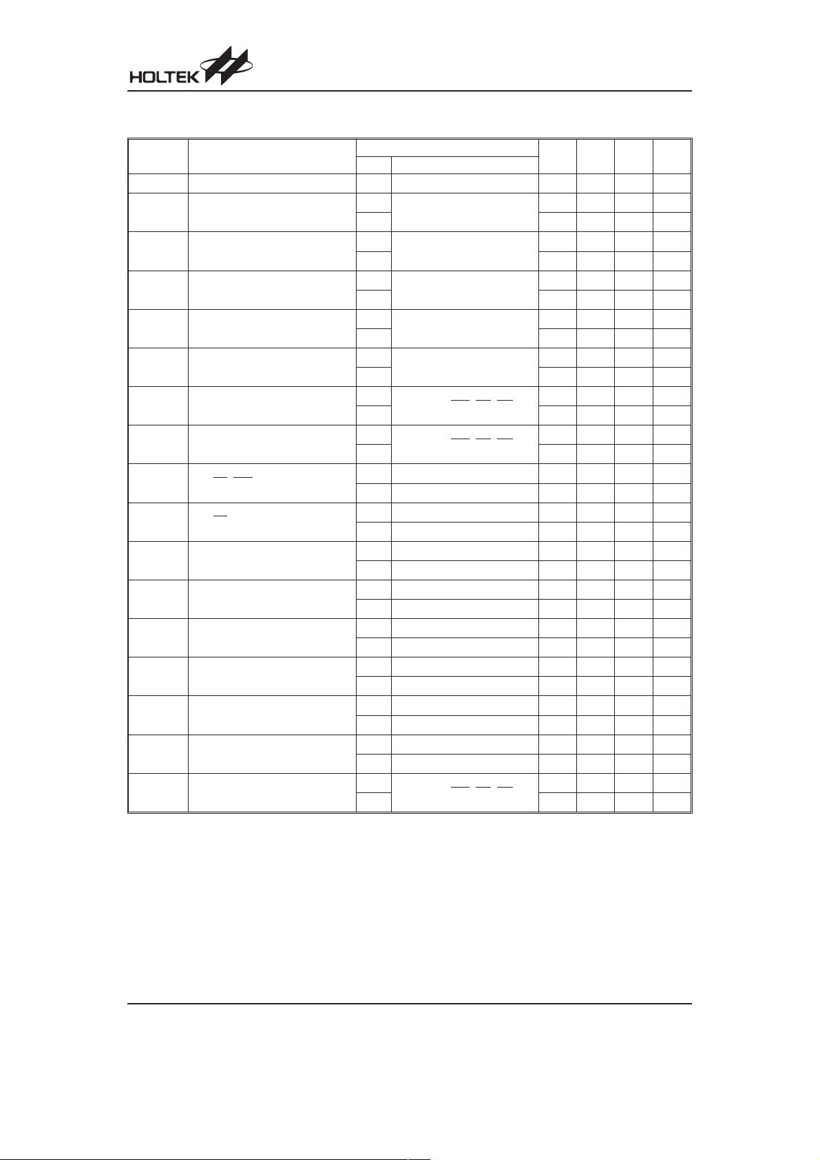
D.C. Characteristics
Symbol Parameter
V
I
DD1
I
DD2
I
DD11
I
DD22
I
STB
V
V
I
OL1
I
OH1
I
OL2
I
OH2
I
OL3
I
OH3
I
OL4
I
OH4
R
DD
IL
IH
PH
Operating Voltage
Operating Current
Operating Current
Operating Current
Operating Current
Standby Current
Input Low Voltage
Input High Voltage
BZ, BZ, IRQ Sink Current
BZ, BZ Source Current
DB0~DB3 Sink Current
DB0~DB3 Source Current
LCD Common Sink Current
LCD Common Source Current
LCD Segment Sink Current
LCD Segment Source Current
Pull-high Resistor
Test Conditions
V
DD
Conditions
¾¾
3V
No load/LCD ON
On-chip RC oscillator
5V
3V
No load/LCD ON
Crystal oscillator
5V
3V
No load/LCD OFF
On-chip RC oscillator
5V
3V
No load/LCD OFF
Crystal oscillator
5V
3V
No load, Power down mode
5V
3V
DB0~DB3, WR,CS,RD
5V 0
3V
DB0~DB3, WR,CS,RD
5V 4.0
V
3V
5V
3V
5V
3V
5V
3V
5V
3V
5V
3V
5V
3V
5V
3V
5V
3V
5V 60 125 210
=0.3V
OL
=0.5V
V
OL
V
=2.7V
OH
=4.5V
V
OH
V
=0.3V
OL
=0.5V
V
OL
V
=2.7V
OH
=4.5V
V
OH
V
=0.3V
OL
=0.5V
V
OL
V
=2.7V
OH
=4.5V
V
OH
V
=0.3V
OL
=0.5V
V
OL
V
=2.7V
OH
=4.5V
V
OH
DB0~DB3, WR,CS,RD
Min. Typ. Max. Unit
2.7
¾
¾
¾
¾
¾
¾
¾
¾
5.2 V
¾
150 250
250 370
135 200
200 300
15 30
50 70
210
310
¾¾
¾¾
0
2.4
¾
¾
¾
0.6 V
1.0 V
¾
1.2 2.5
36
-0.9 -1.8 ¾
-2 -4 ¾
1.2 2.5
36
-0.9 -1.8 ¾
-2 -4 ¾
80 160
180 360
-40 -80 ¾mA
-90 -180 ¾mA
50 100
120 240
-30 -60 ¾mA
-70 -140 ¾mA
150 250 410
Ta=25°C
mA
mA
A
m
mA
mA
mA
mA
mA
1
mA
2
mA
3V
5V
mA
¾
mA
¾
mA
mA
mA
¾
mA
¾
mA
mA
¾mA
¾mA
¾mA
¾mA
kW
kW
Rev. 1.20 6 November 10, 2005
 Loading...