1/2 Duty VFD Digital Clock
Features
·
VFD display 12 hour clock function
·
Directly drive VFD panels at 1/2 Duty cycle
·
4.194304MHz crystal oscillation
·
Zero adjust function
General Description
The HT16562 provides direct drive to VFD panels to im
plement a 12 hour clock function. Obtaining its time
base from a 4.194304MHz crystal oscillation source
and in having a wide operating voltage due to its internal
voltage regulator, the device also contains a host of
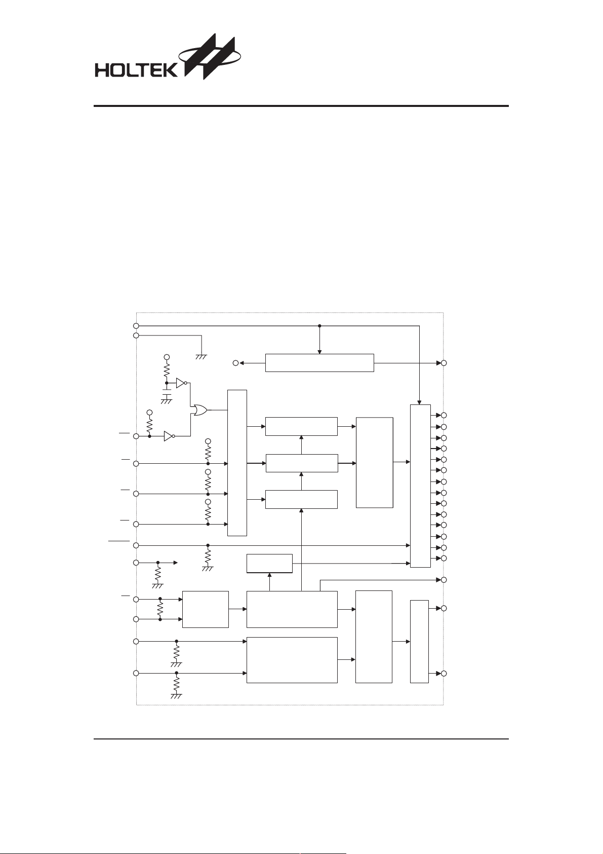
Block Diagram
V C C
V S S
V
D D
V
D D
HT16562
·
Integrated voltageregulator permitswide 4Vto 18V
operating voltage range
·
Four levels of illumination control function
·
30-pin SSOP package
other features. These include a choice of adjustment
modes, including single push increment or 2Hz fast for
ward functions. Additional features are provided in the
form of Blank control, Zero adjustment and four levels of
illumination control.
V o l t a g e R e g u l a t o r C i r c u i t
-
V D D
B L A N K
T E S T
D I M 1
D I M 2
V
D D
1 a , 3 a
A / C
Z A
H S
M S
X T
X T
V
D D
V
D D
V
D D
O s c i l l a t o r
T i m e A d j u s t m e n t
H o u r C o u n t e r
M i n u t e C o u n t e r
S e c o n d C o u n t e r
C o l o n
F r e q u e n c y
F r e q u e n c y D r i v e r C i r c u i t
B r i g h t n e s s A d j u s t m e n t
S e g m e n t
D e c o d e r
G r i d
D e c o d e r
S e g m e n t O u t p u t D r i v e r
G r i d O u t p u t D r i v e r
1 b , 3 b
1 c , 3 c
1 d , 3 d
1 e , 3 e
1 f , 3 f
1 g , 3 g
2 a , 2 d
2 b , 4 b , 4 c
2 c , c o l *
2 c , c o l ' *
2 e
2 f
2 g
6 4 H z
G R 1
G R 2
Note: ²*² col indicates a blink colon and col¢ indicates a continuous light colon.
Rev. 1.00 1 March 28, 2007

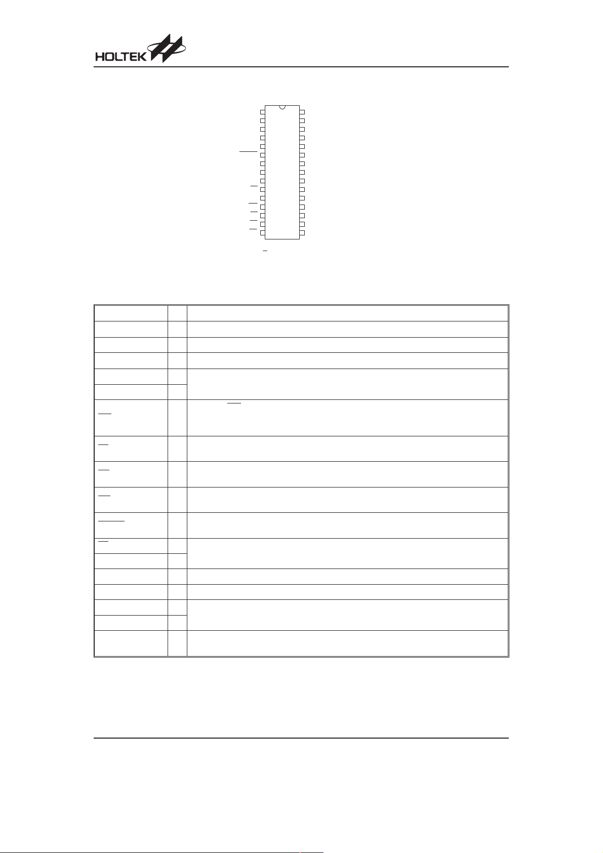
Pin Assignment
HT16562
G R 1
3 0
2 a , 2 d
2 9
2 b , 4 b , 4 c
2 8
2 f
2 7
2 c , c o l *
2 6
2 c , c o l ' *
2 5
2 e
2 4
2 g
2 3
2 2
1 d , 3 d
1 e , 3 e
2 1
1 c , 3 c
2 0
1 g , 3 g
1 9
1 f , 3 f
1 8
1 b , 3 b
1 7
1 a , 3 a
1 6
6 4 H z
T E S T
B L A N K
D I M 1
D I M 2
G R 2
V C C
V D D
V S S
A / C
M S
X T
X T
Z A
H S
1
2
3
4
5
6
7
8
9
1 0
1 1
1 2
1 3
1 4
1 5
H T 1 6 5 6 2
3 0 S S O P - A
Note: ²*² col indicates a blink colon and col¢ indicates a continuous light colon.
Pin Description
Pin Name I/O Description
VCC
VDD O Built-in regulator voltage output pin for the device internal circuits.
VSS
DIM1 I
DIM2 I
A/C
ZA
HS
MS
BLANK
XT
XT I
TEST I IC test pin - should be left open or kept at a low level
64Hz O 64Hz signal output pin for oscillation frequency adjustment
GR1 O
GR2 O
1a,3a ~
2b,4b,4c
High voltage power supply pin.
¾
Ground pin.
¾
Illumination level control pins.
Internally connected to pull-down resistors.
When the A/C
I
The reset pulse width should be more than 2ms.
pin is low, the internal circuits are reset.
Internally connected to a pull-high resistor.
Zero Adjustment pin.
I
Internally connected to a pull-high resistor.
Hour Adjustment pin.
I
Internally connected to a pull-high resistor.
Minute Adjustment pin.
I
Internally connected to a pull-high resistor.
When low the Blank input pin will extinguish the display.
I
Internally connected to a pull-down resistor.
O
Crystal oscillator pin
Grid output pins for 1/2 duty VFD
O Segment output pins for 1/2 duty VFD
Rev. 1.00 2 March 28, 2007

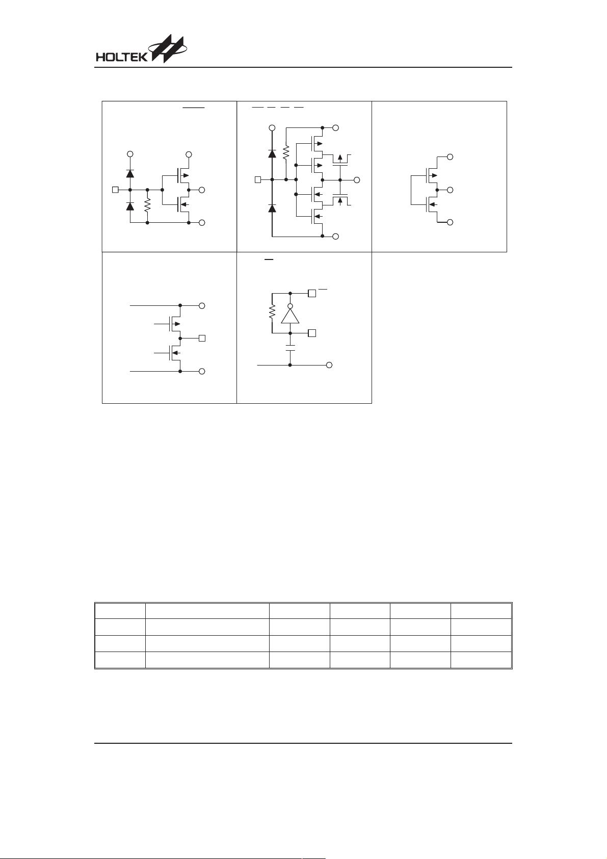
Approximate Internal Connections
HT16562
D I M 1 , D I M 2 , T E S T , B L A N K
V
C C
1 a , 3 a ~ 1 g , 3 g ; 2 a , 2 d ~ 2 g ;
G R 1 , G R 2
V
A / C , Z A , H S , M S
V
C C
D D
V S S
X T , X T
V
V S S
C C
( O s c i l l a t o r O u t p u t )
( O s c i l l a t o r I n p u t )
V
D D
V S S
X T
X T
V S S
6 4 H z
V
V S S
D D
Absolute Maximum Ratings
Logic Supply Voltage .................VSS-0.3V to VSS+6.5V
High Input Voltage .....................V
Logic Input Voltage ....................V
Driver Output Voltage..........................V
-0.3V to VCC+0.3V
SS
-0.3V to VDD+0.3V
SS
-0.3V to V
SS
CC
Driver Output Current (Grid Driver) ......-7mA to +20mA
Driver Supply Voltage .................V
High Output Voltage ..................V
Logic Output Voltage .................V
Driver Output Current (Segment Driver) -10mA to +2mA
Storage Temperature..........................-55°C to +150°C
Operating Temperature.........................-40°Cto+85°C
Note: These are stress ratings only. Stresses exceeding the range specified under ²Absolute Maximum Ratings² may
cause substantial damage to the device. Functional operation of this device at other conditions beyond those listed
in the specification is not implied and prolonged exposure to extreme conditions may affect device reliability.
-0.3V to VSS+20V
SS
-0.3V to VCC+0.3V
SS
-0.3V to VDD+0.3V
SS
Recommended Operating Conditions
Symbol Parameter Min. Typ. Max. Unit
V
f
OSC
t
OP
CC
Power Supply Voltage 4
Oscillation Frequency
Operating Temperature
-40 ¾
¾
¾
4.194304
18 V
¾
MHz
85
°C
Rev. 1.00 3 March 28, 2007
 Loading...