

Holtek Semiconductor Inc HT16220 Datasheet
RAM Mapping 32´8 LCD Controller for I/O mC
Features
Operating voltage: 2.7V~5.2V
·
External Crystal 32.768kHz oscillator
·
1/4 bias, 1/8 duty, frame frequency is 64Hz
·
Max. 32´8 patterns, 8 commons, 32 segments
·
Built-in internal resistor type bias generator
·
3-wire serial interface
·
8 kinds of time base/WDT selection
·
Time base or WDT overflow output
·
Built-in LCD display RAM
·
R/W address auto increment
·
General Description
HT16220 is a peripheral device specially de
signed for I/O type mC used to expand the dis
play capability. The max. display segment of
the device are 256 patterns (32´8). It also sup
ports serial interface, buzzer sound, watchdog
timer or time base timer functions. The
HT16220 is a memory mapping and
multi-function LCD controller. The software
HT16220
Two selectable buzzer frequencies
·
(2kHz/4kHz)
Power down command reduces power
·
consumption
Software configuration feature
·
Data mode and Command mode instructions
·
Three data accessing modes
·
VLCD pin to adjust LCD operating voltage
·
Cascade application
·
configuration feature of the HT16220 make it
suitable for multiple LCD applications includ
ing LCD modules and display subsystems. Only
three lines are required for the interface be
tween the host controller and the HT16220.
The HT162X series have many kinds of prod
ucts that match various applications.
-
-
-
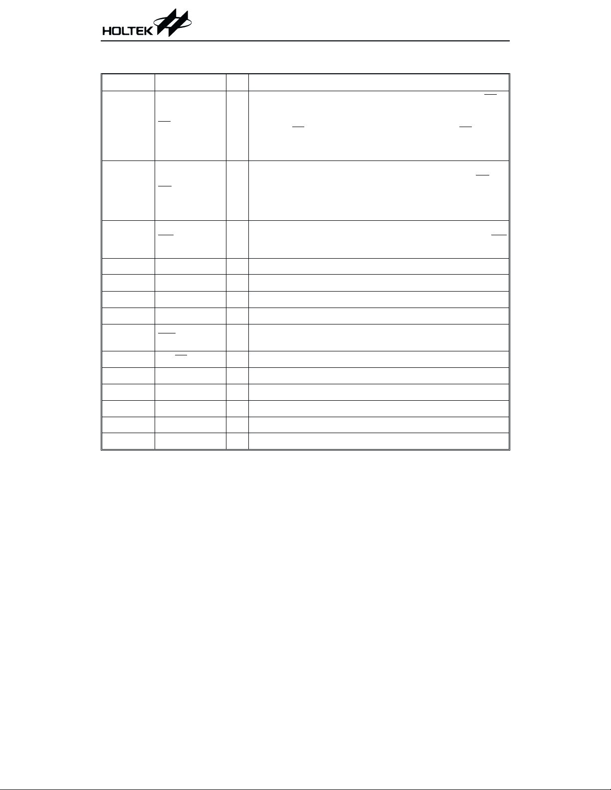
Selection Table
HT162X HT1620 HT1621 HT1622 HT16220 HT1623 HT1625 HT1626 HT1627 HT16270
COM
SEG
Built-in Osc.
Crystal Osc.
448 8 8 8 16 16 16
32 32 32 32 48 64 48 64 64
ÖÖ ÖÖÖÖ
ÖÖ
Ö
1 April 21, 2000
ÖÖÖ Ö
Block Diagram
HT16220
OSCO
OSCI
CS
RD
WR
DATA
VDD
VSS
BZ
Tone Frequency
BZ
Pin Assignment
CS
NC
RD
WR
DATA
VSS
VDD
VLC D
IR Q
BZ
BZ
NC
OSCO
OSCI
T1
T2
T3
NC
COM 0
C ontrol
and
Tim ing
Circuit
G enerator
SEG30
SEG31
63
64
1
2
3
4
5
6
7
8
9
10
11
12
13
14
15
16
17
18
202122
19
W atchdog Tim er
Tim e B ase G enerator
SEG24
SEG25
SEG26
SEG27
SEG28
SEG29
57
58
59
60
61
62
H T16220
64 Q FP
23
242526272829303132
D ispla y R A M
LCD Driver/
Bias Circuit
and
SEG23
SEG20
SEG21
SEG22
56
53
54
55
NC
52
COM 0
COM 7
SEG 0
SEG 31
VLCD
IR Q
NC
51
50
NC
NC
49
SEG19
48
SEG18
47
SEG17
46
SEG16
45
SEG15
44
SEG14
43
SEG13
42
SEG12
41
SEG11
40
SEG10
39
SEG9
38
SEG8
37
SEG7
36
NC
35
NC
34
SEG6
33
COM 4
COM 1
COM 2
COM 3
COM 5
COM 6
COM 7
SEG0
SEG1
SEG2
SEG3
SEG4
SEG5
2 April 21, 2000
Pad Assignment
CS
RD
WR
DATA
VSS
VDD
VLCD
IR Q
BZ
BZ
OSCO
OSCI
T1
T2
T3
4
5
6
7
8
9
10
11
12
13
14
15
HT16220
SEG 20
SEG 22
SEG 23
SEG 25
SEG 26
SEG 27
SEG 28
SEG 29
SEG 30
SEG 31
51
52
53
54
55
1
2
3
16
17
COM 1
COM 0
50
49
18
COM 2
SEG24
48
19
COM 3
47
46
20
COM 4
SEG 21
(0 ,0 )
21
COM 5
45
44
22
COM 6
23
COM 7
24
SEG 0
25
SEG 1
26
SEG 2
27
SEG 3
28
SEG 4
29
SEG 5
43
42
41
40
39
38
37
36
35
34
33
32
31
30
SEG 6
SEG 19
SEG 18
SEG 17
SEG 16
SEG 15
SEG 14
SEG 13
SEG 12
SEG 11
SEG 10
SEG 9
SEG 8
SEG 7
Chip size: 151 ´ 157 (mil)
2
* The IC substrate should be connected to VDD in the PCB layout artwork.
3 April 21, 2000
Pad Coordinates Unit: mil
Pad No. X Y Pad No. X Y
1
2
3
4
5
6
7
8
9
10
11
12
13
14
15
16
17
18
19
20
21
22 14.66
23 21.29
24 27.92
25 34.55
26 41.18
27 47.81
28 54.44
-68.76 72.04
-68.76 59.71
-68.76
-69.53
-69.70
-69.70
-69.70
-69.70
-69.70 -10.28
-69.70 -23.55
-69.70 -38.93
-69.70 -45.56
-69.70 -56.53
-69.70 -63.83
-69.70 -70.46
-39.57 -71.57
-32.94 -71.57
-20.53 -71.57
-13.90 -71.57
-1.49 -71.57
5.14 -71.57
53.08 31 68.98
39.40 32 68.98
24.82 33 68.98 2.85
18.19 34 68.98 9.48
11.56 35 68.98 16.11
1.36 36 68.98 22.74
-72.33
-72.33
-72.33
-72.33
-72.33
-72.33
-72.33
29 61.07
30 67.70
37 68.98 29.37
38 68.98 36.00
39 68.98 42.63
40 68.98 49.26
41 68.98 55.89
42 68.98 62.52
43 68.98 69.15
44 13.85 72.04
45 7.22 72.04
46 0.60 72.04
47
48
49
50
51
52
53
54
55
-6.03
-12.66
-19.30
-25.92
-32.56
-39.19
-45.81
-52.44
-59.08
-72.33
-72.33
-10.41
-3.78
72.04
72.04
72.04
72.04
72.04
72.04
72.04
72.04
72.04
HT16220
4 April 21, 2000
Pad Description
Pad No. Pad Name I/O Description
Chip selection input with pull-high resistor. When the CS
logic high, the data and command read from or written to the
1CS
2RD
3WR
4 DATA I/O Serial data input/output with pull-high resistor
5 VSS
6 VDD
7 VLCD I LCD operating voltage input pad.
8 IRQ
9, 10 BZ, BZ
11 OSCO O Crystal oscillator output pin
12 OSCI I Crystal oscillator input pin
13~15 T1~T3 I Not connected
16~23 COM0~COM7 O LCD common outputs
24~55 SEG0~SEG31 O LCD segment outputs
HT16220 are disabled. The serial interface circuit is also reset
I
But if the CS
data and command transmission between the host controller
and the HT16220 are all enabled.
READ clock input with pull-high resistor. Data in the RAM of
the HT16220 are clocked out on the rising edge of the RD
nal. The clocked out data will appear on the data line. The host
I
controller can use the next falling edge to latch the clocked out
data.
WRITE clock input with pull-high resistor. Data on the DATA
I
line are latched into the HT16220 on the rising edge of the WR
signal.
Negative power supply, ground
¾
Positive power supply
¾
Time base or watchdog timer overflow flag, NMOS open drain
O
output.
O 2kHz or 4kHz tone frequency output pair
is at logic low level and is input to the CS pad, the
HT16220
is
sig
-
Absolute Maximum Ratings
Supply Voltage ..............................-0.3V to 5.5V
Input Voltage ................V
Note: These are stress ratings only. Stresses exceeding the range specified under ²Absolute Maxi
mum Ratings² may cause substantial damage to the device. Functional operation of this device
at other conditions beyond those listed in the specification is not implied and prolonged expo
sure to extreme conditions may affect device reliability.
-0.3V to VDD+0.3V
SS
Storage Temperature ................-50°Cto125°C
Operating Temperature .............-25°Cto75°C
5 April 21, 2000
-
-
HT16220
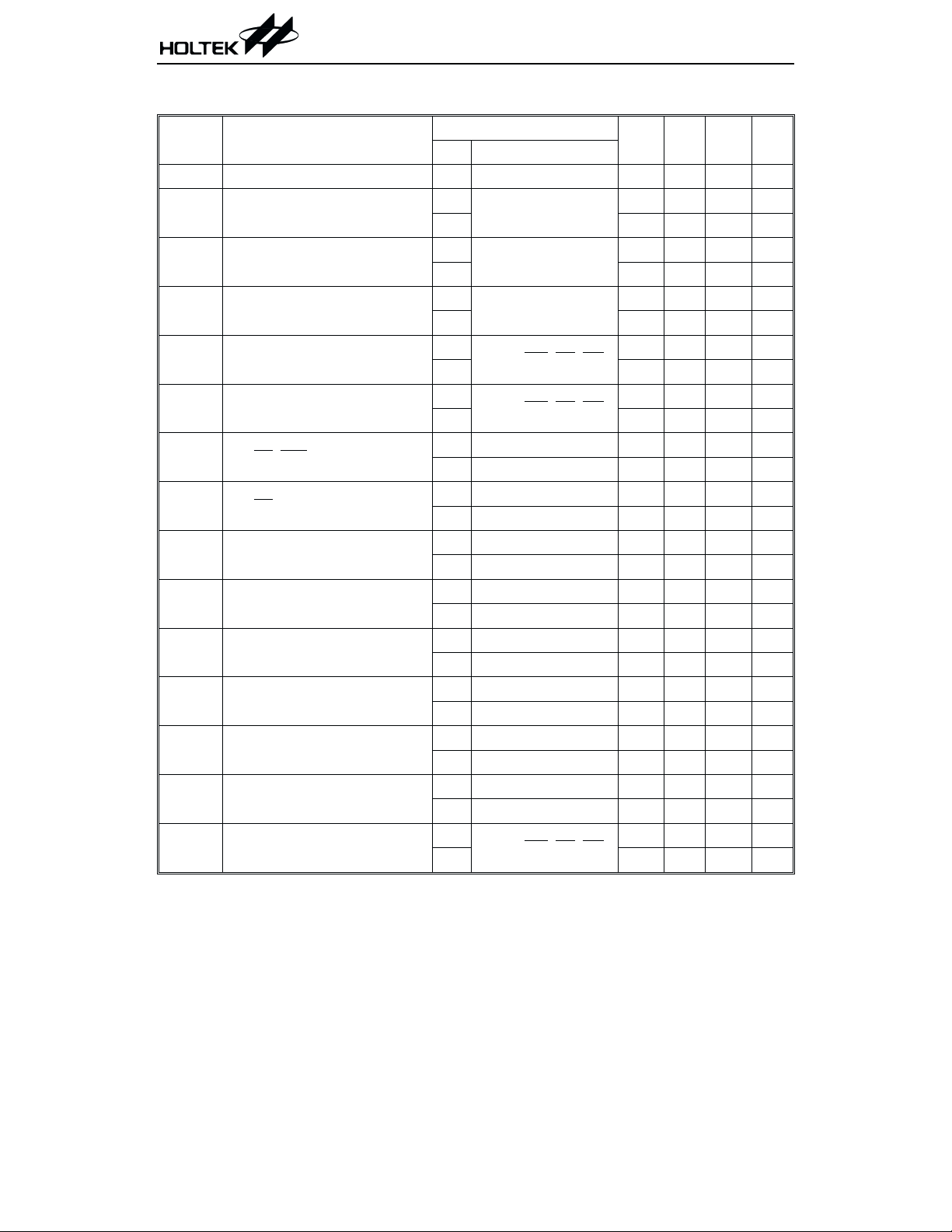
D.C. Characteristics
Symbol Parameter
V
I
I
I
V
V
I
I
I
I
I
I
I
I
R
DD
DD1
DD2
STB
IL
IH
OL1
OH1
OL1
OH1
OL2
OH2
OL3
OH3
PH
Operating Voltage
Operating Current
Operating Current
Standby Current
Input Low Voltage
Input High Voltage
BZ, BZ, IRQ
BZ, BZ
DATA
DATA
LCD Common Sink Current
LCD Common Source Current
LCD Segment Sink Current
LCD Segment Source Current
Pull-high Resistor
Test Conditions
V
DD
Conditions
¾¾
3V
No load LCD ON
Crystal oscillator
5V
3V
No load/LCD OFF
Crystal oscillator
5V
3V
No load
Power down mode
5V
3V
DATA, WR,CS,RD
5V 0
3V
DATA, WR,CS,RD
5V 4.0
V
3V
5V
3V
5V
3V
5V
3V
5V
3V
5V
3V
5V
3V
5V
3V
5V
3V
5V 50 100 150
=0.3V
OL
=0.5V
V
OL
V
=2.7V
OH
V
=4.5V
OH
V
=0.3V
OL
=0.5V
V
OL
V
=2.7V
OH
V
=4.5V
OH
V
=0.3V
OL
=0.5V
V
OL
V
=2.7V
OH
V
=4.5V
OH
V
=0.3V
OL
=0.5V
V
OL
V
=2.7V
OH
V
=4.5V
OH
DATA, WR,CS,RD
Min. Typ. Max. Unit
2.7
¾
5.2 V
¾¾
¾¾
¾¾
¾¾
0
18
216
0.6 V
¾
1.0 V
¾
¾
¾
¾
2.4
¾
0.9 1.8
1.7 3
-0.9 -1.8 ¾
-1.7 -3 ¾
200 450
250 500
-200 -450 ¾mA
-250 -500 ¾mA
15 40
100 200
-15 -30 ¾mA
-45 -90 ¾mA
15 30
70 150
-6 -13 ¾mA
-20 -40 ¾mA
100 200 300
Ta=25°C
50
mA
65
mA
20
mA
30
mA
mA
mA
3V
5V
mA
¾
mA
¾
mA
mA
¾mA
¾mA
¾mA
¾mA
¾mA
¾mA
kW
kW
6 April 21, 2000
 Loading...