

2×20 Channel LCD Driver
Features
•
Operating voltage: 2.7V ~5.2V
•
LCD driving voltage: 3.0V~5.0V
•
40 internal LCD drivers available
•
Bias voltage: static to 1/5 bias
Applications
•
Electronic dictionaries
•
Portable computers
General Description
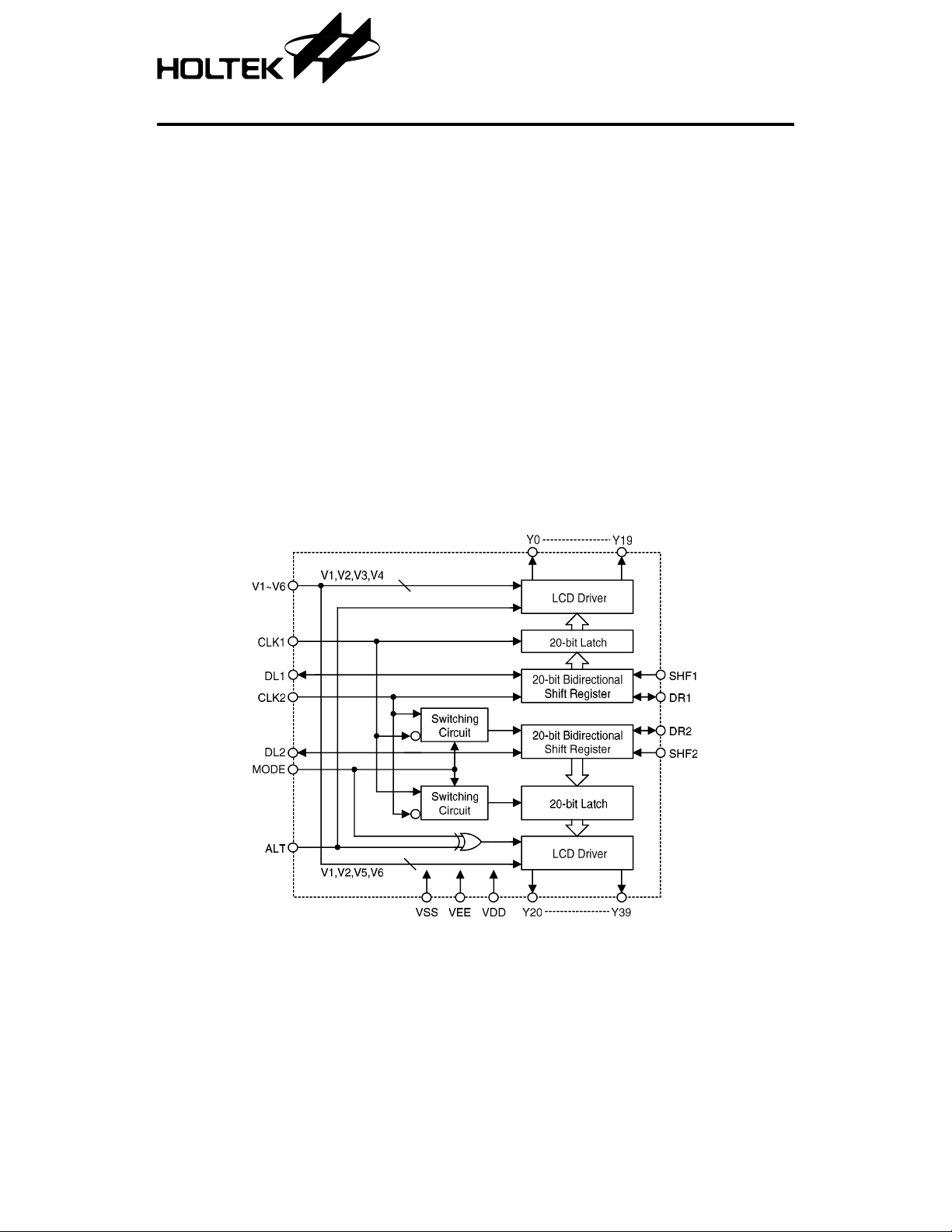
The HT1608L is an LCD driver LSI with 40
output channel s using CMOS technolo gy. It is
equipped with two sets of 20-bit bidire ctional
shift registers, 20-bi t data latches, 20-bit LCD
drivers, and logic control circuits.
The HT1608 can convert serial data received
Block Diagram
HT1608L
•
LCD driver with serial /parallel conversion
function
•
Common or segment driver output by
selection
•
Remote controllers
•
Calculators
from an LCD control ler into parallel da ta and
send out LCD d riving waveforms to the LCD
panel. The HT1608L is designed for general
purpose LCD drivers. It can drive both static
and dynamic drive LCDs. Th e chip can be applied to a common driver or a segment driver.
1 27th Aug ’98
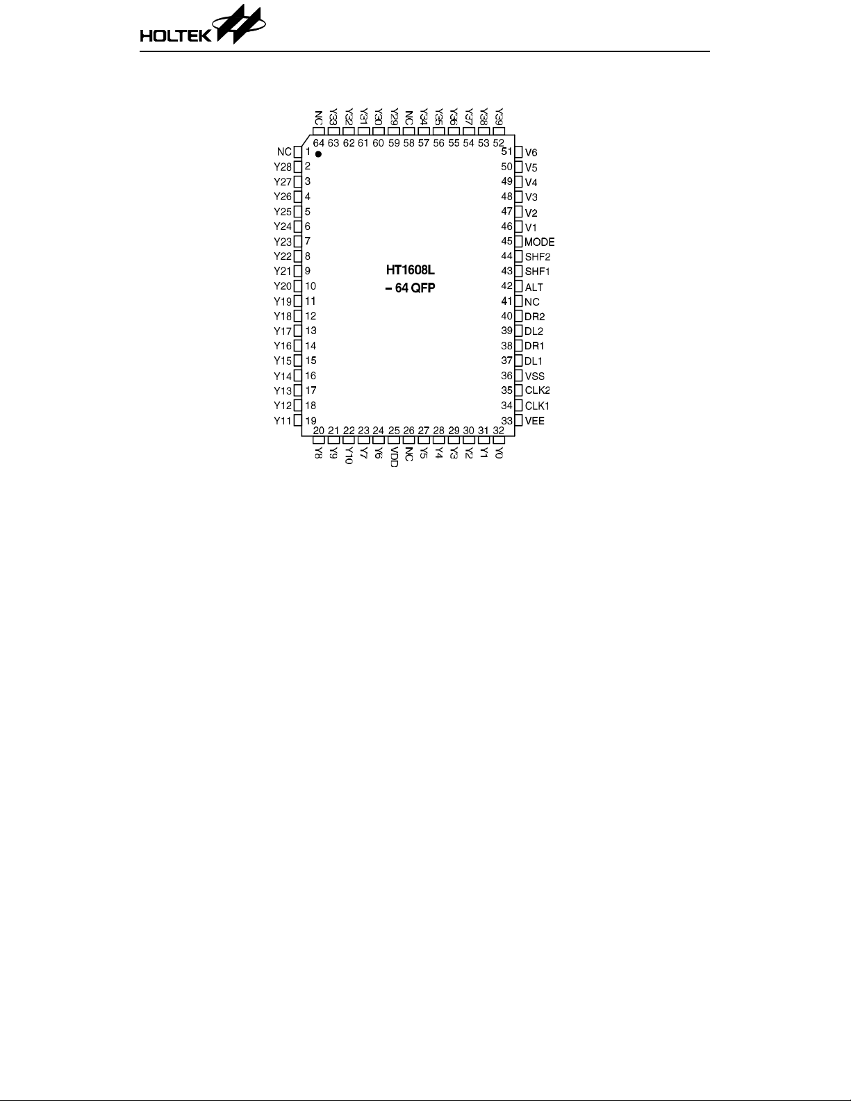
Pin Assignment
HT1608L
2 27th Aug ’98
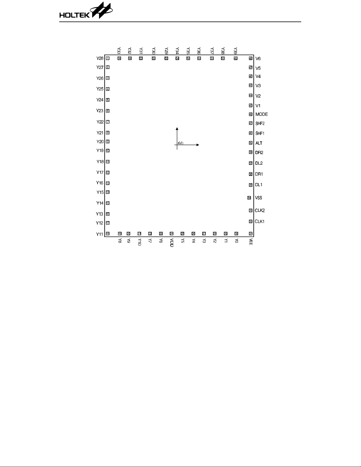
Pad Assignment
HT1608L
Chip size: 101 × 115 (mil)
* The IC substrate should be connected to VDD in the PCB layout artwork.
3 27th Aug ’98
2
HT1608L
Pad Coordinates Unit: mil
Pad No. X Y Pad No. X Y
1 –44.54 51.94 31 44.12 –51.38
2 –44.54 45.86 32 44.12 –42.97
3 –44.54 39.78 33 44.12 –36.93
4 –44.54 33.70 34 42.33 –29.62
5 –44.54 27.63 35 44.12 –22.31
6 –44.54 21.55 36 44.12 –16.28
7 –44.54 15.47 37 44.12 –10.67
8 –44.54 9.39 38 44.12 –4.63
9 –44.54 3.32 39 44.12 0.98
10 –44.54 –2.76 40 44.12 7.01
11 –44.54 –8.84 41 44.12 12.62
12 –44.54 –14.92 42 44.12 18.66
13 –44.54 –21.00 43 44.12 24.31
14 –44.54 –27.07 44 44.12 29.83
15 –44.54 –33.15 45 44.12 35.36
16 –44.54 –39.23 46 44.12 40.88
17 –44.54 –45.31 47 44.12 46.41
18 –44.54 –51.38 48 44.12 51.94
19 –36.55 –51.38 49 31.28 51.94
20 –29.92 –51.38 50 24.74 51.94
21 –23.29 –51.38 51 18.19 51.94
22 –16.66 –51.38 52 11.65 51.94
23 –10.03 –51.38 53 5.10 51.94
24 –3.40 –51.38 54 –1.45 51.94
25 3.23 –51.38 55 –7.99 51.94
26 9.86 –51.38 56 –14.53 51.94
27 16.49 –51.38 57 –21.08 51.94
28 23.12 –51.38 58 –27.63 51.94
29 29.75 –51.38 59 –34.17 51.94
30 36.38 –51.38
Pad Description
Pad No. Pad Name I/O Description
1~9 Y28~Y20 O LCD driver outputs for channel 2
10~23 Y19~Y6 O LCD driver outputs for channel 1
24 VDD — Power supply ( positive )
25~30 Y5~Y0 O LCD driver ou tputs for channel 1
31 VEE I LCD power supply
32 CLK1 I
Latch signal for channel 1 on the falling edge
CLK1 is used for channel 2 when MODE is set to V
4 27th Aug ’98
(Note 1 )
SS

HT1608L
Pad No. Pad Name I/O Description
33 CLK2 I
34 VSS — Power supply (ground)
35 DL1 I/O Data input/output of channel 1 shift register
36 DR1 I/O Data input/output of channel 1 shift register
37 DL2 I/O Data input/output of channel 2 shift register
38 DR2 I/O Data input/output of channel 2 shift register
39 ALT I Alternate signal input for LCD driving waveform
40 SHF1 I Shift direction selection of channel 1 shift register (Note 2)
41 SHF2 I Shift direction selection of channel 2 shift register (Note 2)
42 MODE I Mode select signal of channel 2 (Note 3)
43, 44 V1, V2 I LCD bias supply voltage for channels 1 and 2
45, 46 V3, V4 I LCD bias supply voltage for channel 1
47, 48 V5, V6 I LCD bias supply voltage for channel 2
49~59 Y39~Y29 O LCD driver outputs for channel 2
Shift signal for channel 1 on the falling edge and used for channel 2
when MODE is set to V
(Note 1)
SS
Note 1: Data is processed on the clock falling or rising edge as shown in the following table.
MODE= L (V
MODE= H (V
SS
DD
)
)
5 27th Aug ’98

HT1608L
Note 2 : Shift direction of channel 1 and 2
Shift Direction of Channel 1 (Channel 2)
SHF1 (SHF2) DL1 (DL2) DR1 (DR2)
HOUTIN
LINOUT
Note 3 :
The output lev els of channel 1 and 2 are decided by t he combination of MODE, ALT
and latched data. Refer to the following table:
MODE Latched Data ALT
HV1 V2
LV2 V1
HV3 V6
(V
H
DD
H
)
L
LV4 V5
HV1 V1
LV2 V2
HV3 V5
L
(V
)
SS
H
L
LV4 V6
Channel 1
(Y0~Y19)
Channel 2
(Y20~Y39)
6 27th Aug ’98

HT1608L
Absolu te Maxim um Ratings *
Supply Voltage........................ .... ..–0.3V to 5.5V Storage Temperature.................–50°C to 125°C
Input Voltage................. V
*Note: These are stress ra tings on ly. Stresses exceeding the range specifie d under “Ab solute Maxi -
mum Ratings” ma y cause substantial damage to the device. Functional operation of this
device at other conditions beyond those listed in the specification is not implied and prolonged
exposure to extreme condition s may affect device reliability.
D.C. Characteristics Ta=25°C
–0.3V to VDD+0.3V Operating Temperature...............–20°C to 70°C
SS
Symbol Parameter
V
DD
I
DD
I
STB
f
CLK2
tw
V
IL
V
IH
V
OL
V
OH
V
LCD
CLK
Operating Voltage — — 2.7 — 5.2 V
Operating Current 5V No load — 100 300 µA
Standby Current 5V — — 1 5 µA
Data Shift Frequency 5V — — — 400 kHz
Clock Pulse Width 5V — 800 — — ns
“L” Input Voltage 5V — — — 1 V
“H” Input Voltage 5V — 4 — — V
“L” Output Voltage 5V IOL=+0.4mA — — 0.4 V
“H” Output Voltage 5V IOH=–0.4mA 4.6 — — V
LCD Driving Voltage — VDD–V
Test Conditions
V
DD
Conditions
EE
Min. Typ. Max. Unit
3—5.0V
7 27th Aug ’98

HT1608L
Functional Description
Both channel 1 and 2 used as segment drivers (MODE=L)
When both channel 1 and 2 of the HT1608L are used as segment drivers, they will shift data on the
falling edge of CLK2 and shift latch data on the falling edge of CLK1. V3 and V5 or V4 and V6 are
shortened in the application circuit as shown in the following figure.
Both ch annel 1 an d 2 used as comm o n drivers (MODE=L )
When both channe l 1 an d 2 o f the HT1 608L are used a s co mm on d rivers, the MODE is s et low a nd
the signals (CLK1, CLK2, FRAME) from the controller are connected as shown in the following
figure.
8 27th Aug ’98

HT1608L
Channel 1 used as a segment driver an d ch an ne l 2 as a com m o n drive r (MOD E =H )
When channel 2 is used as a common drive r, MODE is connected to VDD. Channel 2 will shift data
on the rising edge of CLK1 and shift latch data on the rising edge of CLK2.
Static driver
When the HT1608 L is used as a static drive r, data is transferred on the falling edge of CLK2 and
latched on the falling edge of CLK1. The frequency of CLK1 becomes the frame frequency of the LCD
driver. The frequency of ALT has to be twice the frequency of CLK1. ALT has to be synchronized on
the falling edge of CLK1.
The power supply for the LCD driver is used by shortening V1, V4 and V6 or V2, V3 and V5. One of
the LCD output te rmi na ls can be used as a com mo n o utpu t . The app licati on circui t connecti on s are
shown below:
9 27th Aug ’98

Timing Diagrams
Segment data waveform (1/8 duty)
HT1608L
10 27th Aug ’98

HT1608L
Common data wav eform (a typical wav eform of chan ne l 2 as a COMM O N drive r, 1/8 duty)
11 27th Aug ’98

Application Circuits
HT1608L
12 27th Aug ’98
 Loading...