Features
Operating voltage: 2.0V~5.5V
·
Maximum input serial clock: 500kHz at
·
V
=2V, 2MHz at VDD=5V
DD
Operating current: less than 400nA at 2V,
·
less than 1.2mAat5V
TTL compatible
·
-
VIH: 2.0V~VDD+0.3V at VDD=5V
-
VIL: -0.3V~+0.8V at VDD=5V
Applications
Microcomputer serial clock
·
General Description
The HT1380/HT1381 is a serial timekeeper IC
which provides seconds, minutes, hours, day,
date, month and year information. The number
of days in each month and leap years are auto
matically adjusted. The HT1380/HT1381 is de
signed for low power consumption and can
operate in two modes: one is the 12-hour mode
with an AM/PM indicator, the other is the
24-hour mode.
HT1380/HT1381
Serial Timekeeper Chip
Two data transmission modes: single-byte,
·
or burst mode
Serial I/O transmission
·
All registers store BCD format
·
HT1380: 8-pin DIP package
·
HT1381: 8-pin SOP package
Clock and Calendar
·
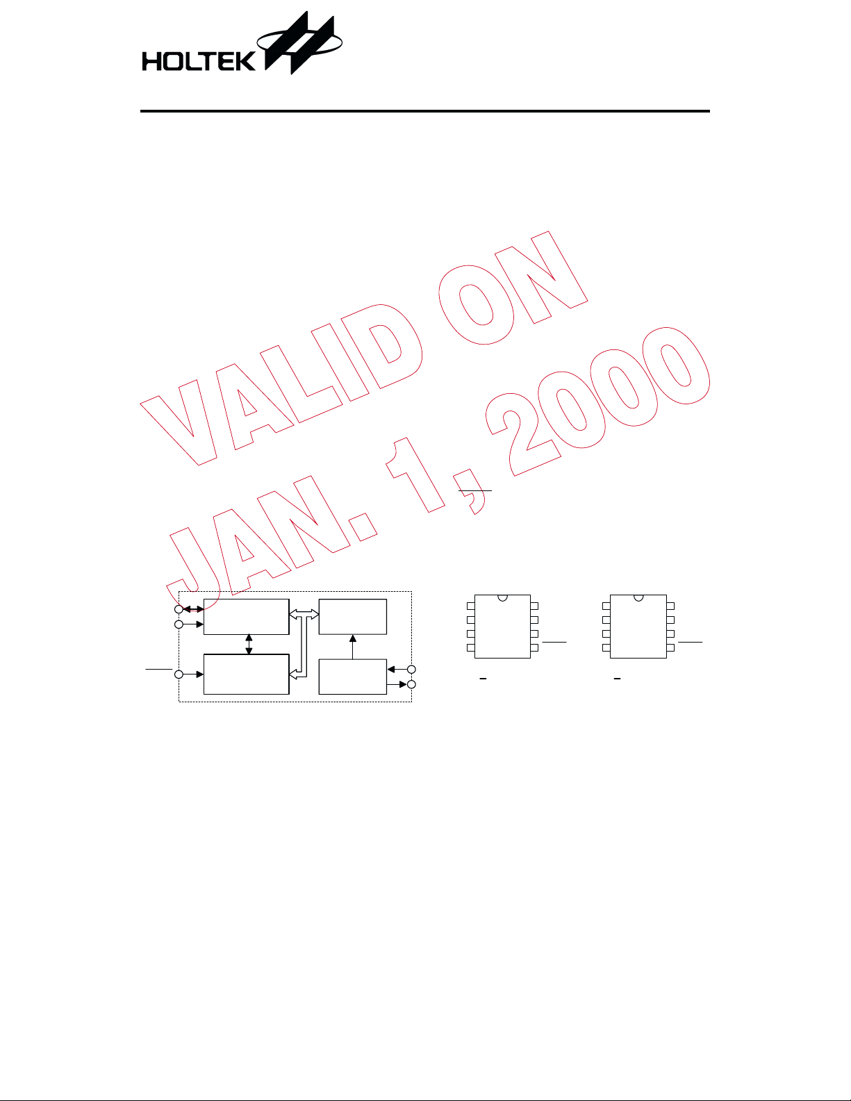
The HT1380/HT1381 has several registers to
store the corresponding information with 8-bit
data format. A 32768Hz crystal is required to
provide the correct timing. In order to minimize
the pin number, the HT1380/HT1381 use a se
rial I/O transmission method to interface with a
microprocessor. Only three wires are required:
(1) REST
livered 1 byte at a time or in a burst of up to 8
bytes.
, (2) SCLK and (3) I/O. Data can be de-
-
Block Diagram Pin Assignment
I/O
SCLK
REST
Data Shift
R egister
Command
C ontrol Logic
R eal Tim e
Clock
O s c illa to r a n d
Divider
Circuit
1
NC
2
X1
3
X2
4
VSS
X1
X2
1 October 2, 1999
H T1380
8 D IP
VDD
8
7
SCLK
I/O
6
REST
5
NC
VSS
X1
X2
1
2
3
4
H T1381
8 S O P
VDD
8
7
SCLK
I/O
6
REST
5

HT1380/HT1381
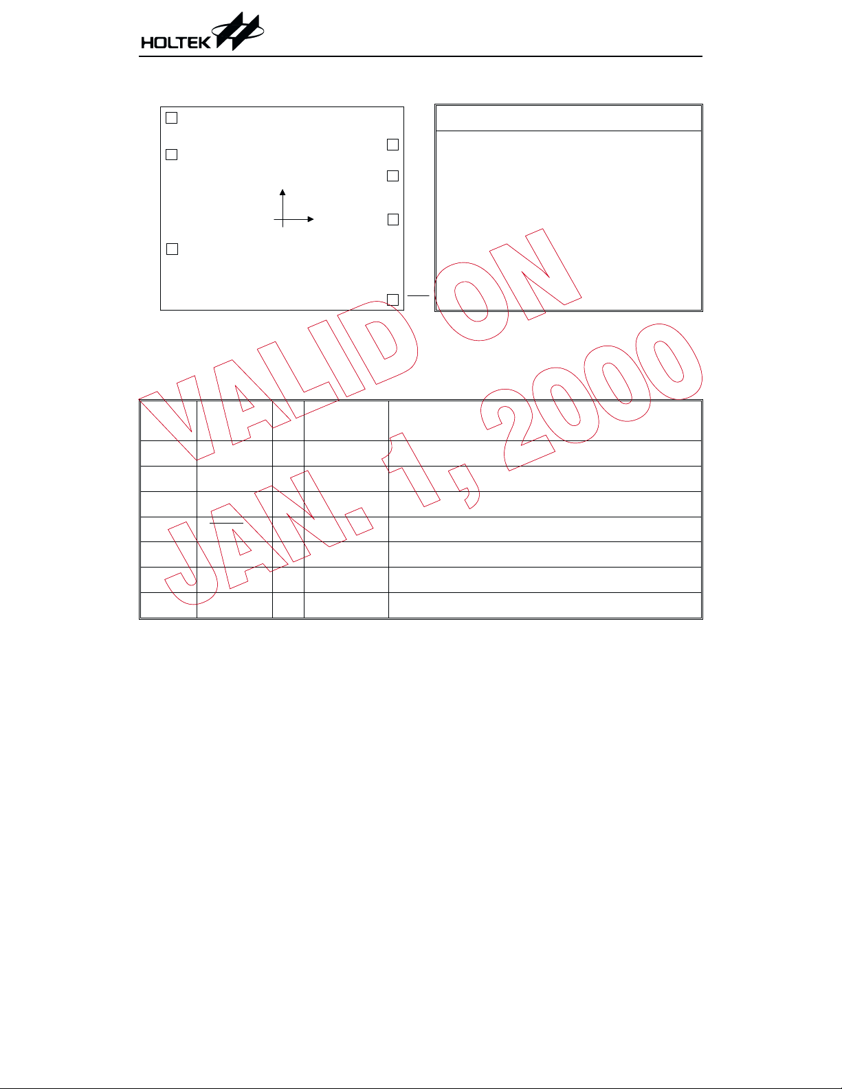
Pad Assignment Pad Coordinates
1
VSS
X1
7
X2
2
(0 ,0 )
3
VDD
6
SCLK
5
I/O
Pad No. X Y
1
2
3
-851.40
-851.40
-844.40 -203.90
4 845.90
5 848.40
6 845.90 332.60
7 844.40 572.60
Chip size: 2010 ´ 1920 (mm)
4
REST
2
* The IC substrate should be connected to VSS in the PCB layout artwork.
Pad Description
Pad No. Pad Name I/O
1 X1 I CMOS 32768Hz crystal input pad
2 X2 O CMOS Oscillator output pad
Internal
Connection
Description
Unit: mm
775.00
494.60
-618.30
-4.30
3 VSS I CMOS Ground pin
4 REST
I CMOS Reset pin with serial transmission
5 I/O I/O CMOS Data input/output pin with serial transmission
6 SCLK I CMOS Serial clock pulse pin with serial transmission
7 VDD I CMOS Power supply pin
Absolute Maximum Ratings
Supply Voltage..............................-0.3V to 5.5V
Input Voltage .................V
-0.3V to VDD+0.3V
SS
Note: These are stress ratings only. Stresses exceeding the range specified under ²Absolute Maxi
mum Ratings² may cause substantial damage to the device. Functional operation of this de
vice at other conditions beyond those listed in the specification is not implied and prolonged
exposure to extreme conditions may affect device reliability.
Storage Temperature.................-50°Cto125°C
Operating Temperature ..................0°Cto70°C
2 October 2, 1999
-
-

HT1380/HT1381
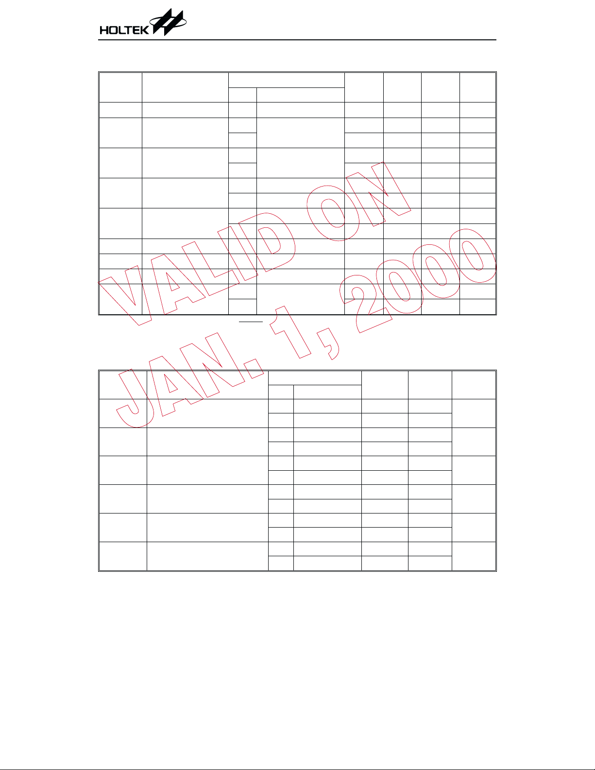
D.C. Characteristics
Symbol Parameter
* I
V
DD
I
STB
I
DD
I
OH
I
OL
V
IH
V
IL
f
OSC
f
SCLK
STB
Operating Voltage
Standby Current
Operating Current
Source Current
Sink Current
²H² Input Voltage
²L² Input Voltage
System Frequency 5V
Serial Clock
is specified with SCLK, I/O, REST open. The clock halt bit must be set to logic 1 (oscillator
disabled).
Test Conditions
V
DD
Conditions
¾¾
2V
5V
2V
5V
2V
5V
2V
5V
5V
5V
No load
V
V
V
V
¾
=1.8V
OH
=4.5V
OH
=0.2V
OL
=0.5V
OL
¾
¾¾¾
32768Hz X¢TAL ¾
2V
5V
¾
Min. Typ. Max. Unit
2
¾
¾¾
¾¾
¾
¾
0.7 1.0
0.7 1.2
-0.2 -0.4 ¾
-0.5 -1.0 ¾
0.7 1.5
2.0 4.0
2
¾¾
32768
¾¾
¾¾
Ta=25°C
5.5 V
100 nA
100 nA
mA
mA
mA
mA
¾
¾
mA
mA
V
0.8 V
¾
Hz
0.5 MHz
2 MHz
A.C. Characteristics
Symbol Parameter
t
DC
t
CDH
t
CDD
t
CL
t
CH
f
CLK
Data to Clock Setup
Clock to Data Hold
Clock to Data Delay
Clock Low Time
Clock High Time
Clock Frequency
Test Conditions
V
Conditions
DD
2V
5V
2V
5V
2V
5V
2V
5V
2V
5V
2V
5V
¾
¾
¾
¾
¾¾
¾¾
¾
¾
¾
¾
¾¾
¾
3 October 2, 1999
Min. Max. Unit
200
50
280
70
¾
¾
¾
¾
800
200
1000
250
1000
250
¾
¾
¾
¾
0.5
D.C. 2.0
Ta=25°C
ns
ns
ns
ns
ns
MHz
 Loading...