

3 1/2 Digit Timer + Watch
Features
A real time watch
·
A 20-hour adjustable range setting
·
count-down timer
20-minute count-up display cycle time
·
20 hours of count-up time maximum
·
Auto recycle or manual reset the
·
count-down timer by bonding option
Hours and minutes are set independently
·
Real time display in timer mode
·
General Description
The HT1330 is a CMOS fabricated LSI chip de
signed to drive a standard three and 1/2 digit
biplexed LCD for a count-up/down timer in
watch applications. The watch and timer are
based on a 32768Hz quartz crystal oscillator.
The maximum count-down time is 20 hours
with an accuracy of 1 second. The maximum
count-up period is 20 hours, but the LCD will
normally display a maximum period of 19 minutes and 59 seconds. If the user presses switch
²S2², the total count-up time in hours and minutes will be displayed. In the count-up/down
mode, the real time can be seen by pressing
HT1330
5-minute/10-minute pre-alarm
·
DC output and piezo output
·
An internal voltage doubler
·
Busy flag output high in timer counting
·
3 1/2 digit LCD display
·
32768Hz crystal oscillator
·
Single 1.5V battery operation
·
48L-pin QFP package
·
-
switch ²S1² and return to the count-up/down
mode by releasing ²S1².
Once the count-down is finished, the timer can
either automatically recycle the preset time or
manually reset the desired time depending on
the selected bonding-pad option. The forecast
alarm generates 4 alarm sounds at 10 minutes
before set time and 8 alarm sounds at 5 minutes
before set time. The HT1330 can be used as a
parking timer, an alarm timer, a pill box timer,
a kitchen timer, a sports timer, etc.
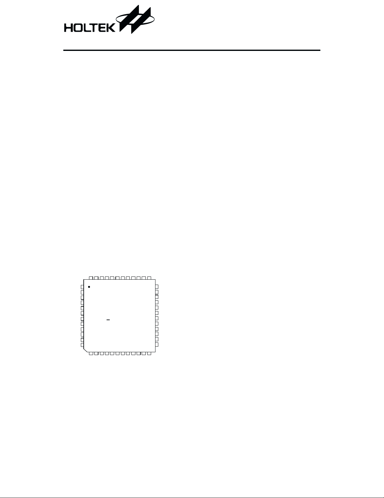
Pin Assignment
BUSY
NC
NCNCNCNCNC
T2
484746 45 44 43 42 41 40 39 3837
1
NC
2
NC
3
NC
4
T1
5
VSS
6
VDD
7
NC
8
OP
BZ
9
BZB
10
S3
11
NC
12
13 1415 161718 19 20 21 222324
NCS2NCS1VEE
H T 1330
48L Q FP
OSC2
OSC1
NC
CAP2NCCAP1NCNCNCCOM 1
COM 2
KD1
36
FE1
35
AG1
34
BC1
33
NC
32
COD3
31
FE2
30
ADG 2
29
BC2
28
FE3
27
AG3
26
25
BC3
1 August 10, 2000
HT1330
Y
2
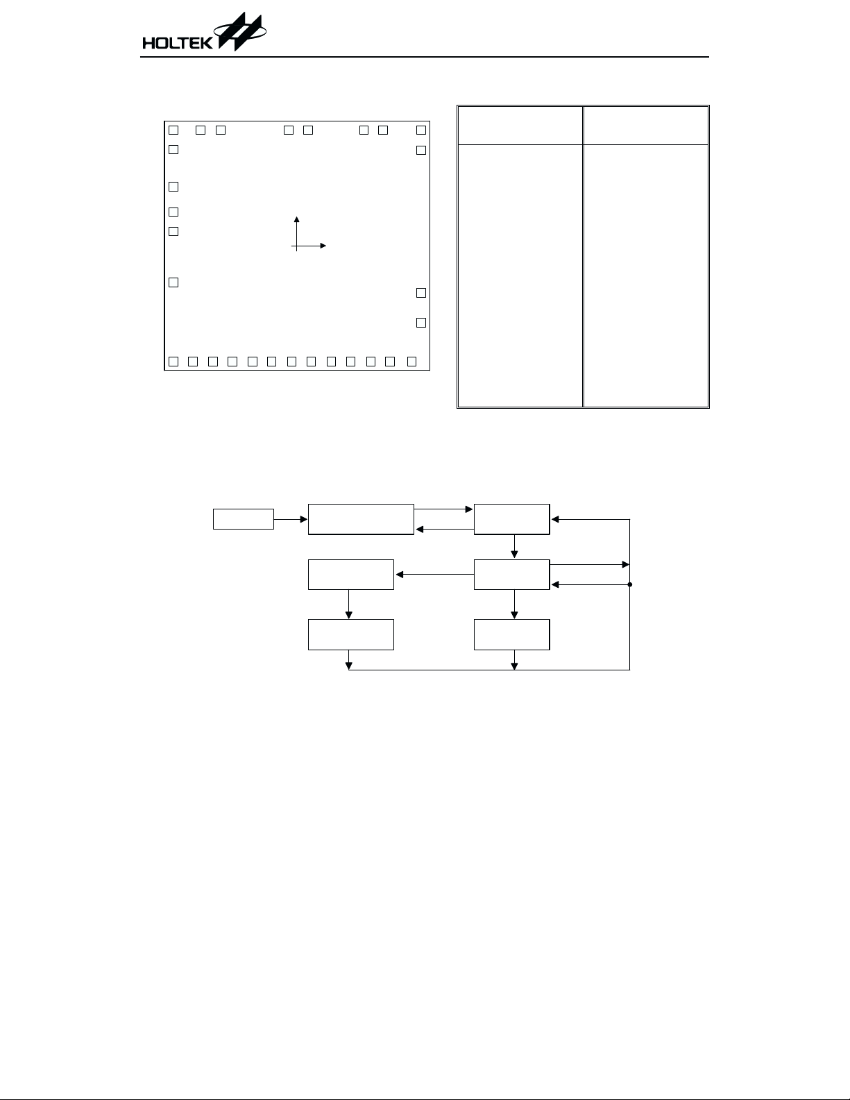
Pad Assignment Pad Coordinates Unit: mil
S3
S2
S1
VEE
CAP2
CAP1
COM 1
BZB
BZ
1
5
6
7
28
29
8
9
10
11
BC2
FE3
AG3
BC3
Chip size: 119 ´ 112 (mil)
12
VDD
OP
26
27
(0 ,0 )
13
14
COD3
FE2
ADG 2
VSS
25
16 2 17 3 18 4 19
15
FE1
AG1
BC1
2
T1
24
T2
23
22
21
20
COM 2
KD1
BUS
OSC
OSC1
Pad
No.
1
-62.7
2
-62.7
3
-62.7
4
-62.7
5
-62.7
6
-62.7 -18.7
7
-62.7 -58.7
8
-52.7 -58.7
9
-42.7 -58.7
10
-32.7 -58.7
11
-22.7 -58.7
12
-12.7 -58.7
13
-2.7 -58.7
14 7.3
15 17.3
XY
58.7 16 27.3
48.7 17 37.3
30.1 18 47.3
17.2 19 58.3
7.3 20 62.7
-58.7
-58.7
Pad
No.
XY
-58.7
-58.7
-58.7
-58.7
-38.8
21 62.7
-23.7
22 62.7 48.6
23 62.7 58.7
24 43.8 58.7
25 33.8 58.7
26 5.8 58.7
27
28
29
-38.6
-48.6
-4.3
58.7
58.7
58.7
* The IC substrate should be connected to VDD in the PCB layout artwork.
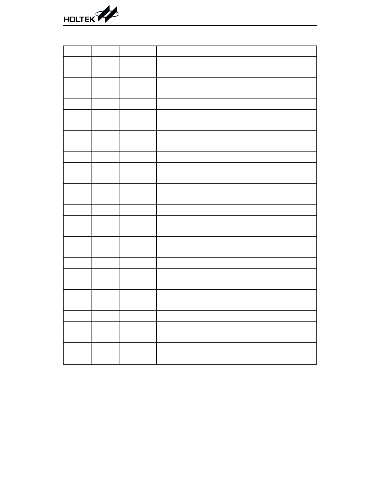
Operational Sequence
Power on
R eal T im e S etting
C ount-dow n
T im e S e ttin g
S3
C ount-dow n Tim er
S1/S 2 or S 1/S2/S 3
Note: S1 for Hour setting
S2 for Minute setting
S3 to Start/Stop the timer
S3>5 seconds into the real time setting mode
S1/S2 to reset the timer to the initial state (0:00)
S1/S2/S3 to return to the real time mode
S3
S3 > 5sec
S1 or S2
R eal T im e
S1/S2
U p/D ow n Tim er
S3
C ount-up Tim er
S1/S 2 or S 1/S2/S 3
S1/S2/S3
S1/S2
2 August 10, 2000
Pin/Pad Description
Pin No. Pad No. Pad Name I/O Description
11 1 S3
14 2 S2
16 3 S1
17 4 VEE
18 5 CAP2
20 6 CAP1
24 7 COM1
25 8 BC3
26 9 AG3
27 10 FE3
28 11 BC2
29 12 ADG2
30 13 FE2
31 14 COD3
33 15 BC1
34 16 AG1
35 17 FE1
36 18 KD1
37 19 COM2
38 20 OSC1
39 21 OSC2
46 22 BUSY
47 23 T2
424T1
5 25 VSS
6 26 VDD
827OP
928BZ
10 29 BZB
I Input to start/stop the timer
I Input for minute setting
I Input for hour setting
Negative voltage supply for LCD display
¾
O For voltage doubling capacitor
O For voltage doubling capacitor
O Common 1 drive
O Segment drive
O Segment drive
O Segment drive
O Segment drive
O Segment drive
O Segment drive
O Segment drive
O Segment drive
O Segment drive
O Segment drive
O Segment drive
O Common 2 drive
I Oscillator input
O Oscillator output
O Timer busy flag, active high
I/O Chip test pin
I/O Fast-test control pin
Negative power supply
¾
Positive power supply
¾
I Option pin for countdown recycle
O Piezo drive
O Piezo drive
HT1330
3 August 10, 2000

Absolute Maximum Rating
HT1330
Supply Voltage.................................-0.3V to 5V
Input Voltage.................V
-0.3V to VDD+0.3V
SS
Storage Temperature.................-50°Cto125°C
Operating Temperature ................-0°Cto70°C
Note: These are stress ratings only. Stresses exceeding the range specified under ²Absolute Maxi
mum Ratings² may cause substantial damage to the device. Functional operation of this de
vice at other conditions beyond those listed in the specification is not implied and prolonged
exposure to extreme conditions may affect device reliability.
Electric Characteristics
Ta=25°C
Test Conditions
Symbol Parameter
V
I
DD
V
I
IN
V
Df/f
I
OHA
f
OUT
I
OHF
DD
EE
STR
Supply Voltage 1.5V
Operating Current 1.5V
Display Voltage 1.25~1.7V
Switch Input Current 1.5V
Osc Starting Voltage
Frequency Stability 1.25~1.7V
Alarm Output Drive Current 1.5V
Alarm Output Frequency 1.5V
Busy Flag Output Drive
Current
V
DD
¾
1.5V
Conditions
¾
fosc=32768Hz
No load
¾-1.2 -1.5 -1.7
V
=VDD
IN
Within 3 secs 1.35
¾¾¾
V
=1.35V
OH
¾¾
=1.35V
V
OH
Min. Typ. Max. Unit
1.25 1.50 1.70 V
¾¾
2
mA
V
5
65
¾
¾¾
mA
V
10 PPM
-480 ¾¾mA
4096
¾
Hz
-480 ¾¾mA
-
-
Functional Description
When power is turned on, all the LCD segments
are illuminated to display ²18:88² and the
alarm sounds 2 seconds.
For fast-test, hold the ²TP1² pin high and the
minute digit will be increased every second.
In the count-down mode, when the time has gone
past the set time and the alarm is stopped, the set
time will remain at its current state or be reset to
0:00 depending on the bonding of the ²OPT² pin
to VDD.
In the timer mode, while the timer is counting,
the actual time can be displayed by pressing ²S1².
Once ²S1² is released, the count-down time will
be shown instead.
In the count-up mode, the LCD display is nor
mally in minutes and seconds where the maxi
mum count-up period is 20 minutes. If ²S2² is
pressed, the LCD display will revert to hours
and minutes and the maximum count-up time
will turn out to be 20 hours.
The timer alarm will sound during the
count-down process as listed below:
4 sounds are generated at 10 minutes before
the set time is up.
8 sounds are generated at 5 minutes before the
set time is up.
4 August 10, 2000
-
-

HT1330
Once the set time is reached, the alarm will
sound 60 seconds unless it is stopped by users
(by pressing S3), in which case the preset time
of the timer will remain unchanged or at 0:00
depending on the status of the option pin.
Pressing any one of the inputs (S1 or S2 or S3)
At 0:00 in the timer mode, the alarm will sound
when S1 and S2 are simultaneously depressed.
This is for the alarm test only.
After the device is powered on, the alarm will
sound two seconds and all segments on the LCD
display panel be illuminated.
will stop the alarm during the period for which
the alarm is sounding.
Output Waveform
10 m in utes before set tim e is up
62.5 m s
2 sec1 sec0 sec
5 m in utes before set tim e is up
62.5 m s
0 sec 1 sec 2 sec
Tim e is up
62.5 m s
62.5 m s
62.5 m s
0 sec 1 sec 60 sec
Tim er busy flag output
VDD
VSS
Tim er is counting up or dow n
5 August 10, 2000

Operational FlowChart
HT1330
Note:
S 1 /S 2 : tw o k e y p re s s e d s y n c h
S1/S 2/S 3: three key pressed on tim e
S 3 > 5 s : S 3 k e y is p re s s e d m o re th a n 5 s
S 1 , S 2 , S 3 : th e k e y is p r e s s e d
#: R epresents 2H z flash
*: R e p re s e n ts 1 H z fla s h
YES
C ount_up M ode C ount_dow n M ode
C ount-up
playing
YES
0:01
B
Power on
18:88
A fter 2 secon d
* 0:00
R eal tim e
setting
S3>5s
NO
* 12:59
S3
S1/S2
0:00
S1/S2
S3
Piezo sounds 2 seconds for alarm test
All segm ent on for LC D test
S1 to adjust hour-digit
S2 to adjust m inute-digit
YES
R eal tim e playing m ode
A
NO
Enter the counter M ode
Alarm test
YES
NO
S1 to adjust hout-digit
C ount_dow n
tim e s e ttin g
S3
#19:59
S2 to adjust m inute-digit
C ount_dow n tim e playing
OP
Bonded
option
NO
S2
S 2 to s h o w th e
count num ber
S 1 /S 2 to B S 1 /S 2 /S 3 to A
S1/S2, S1/S2/
S1, S3,
S3
NO
S1 to display
the real tim e
0:00
S 3 fo r s ta rt/
stop counter
YES
NO
Alarm bibi
A ny key to
press
YES
6 August 10, 2000

HT1330
LCD Format
Application Circuits
V
DD
S3
S2
COM 2
F1/E1
K/D1
K
F1
G1
E1
D1
Piezo
1
28
29
A1/G1
A1
C1
COL/D3
B1/C1
F2/E2
A2
F2
B1
COL
G2
E2
COL
27
D2
26
A3/G3
B2/C2
F3/E3
F3
B2
E3
C2
25
D3
24
G3
B3/C3
A3
23
22
COM 1
B3
C3
Busy
A2D2/G 2
0.01mF
S1
0.01mF
5
H T 1330
6
7
8
9
10
11
12
13
11
Biplexed LC D
14
15
16 2 17 3 18 4 19
7 August 10, 2000
21
20
32768H z
X'TAL
20M
W

HT1330
Holtek Semiconductor Inc. (Headquarters)
No.3 Creation Rd. II, Science-based Industrial Park, Hsinchu, Taiwan, R.O.C.
Tel: 886-3-563-1999
Fax: 886-3-563-1189
Holtek Semiconductor Inc. (Taipei Office)
5F, No.576, Sec.7 Chung Hsiao E. Rd., Taipei, Taiwan, R.O.C.
Tel: 886-2-2782-9635
Fax: 886-2-2782-9636
Fax: 886-2-2782-7128 (International sales hotline)
Holtek Semiconductor (Hong Kong) Ltd.
RM.711, Tower 2, Cheung Sha Wan Plaza, 833 Cheung Sha Wan Rd., Kowloon, Hong Kong
Tel: 852-2-745-8288
Fax: 852-2-742-8657
Copyright Ó 2000 by HOLTEK SEMICONDUCTOR INC.
The information appearing in this Data Sheet is believed to be accurate at the time of publication. However, Holtek
assumes no responsibility arising from the use of the specifications described. The applications mentioned herein are
used solely for the purpose of illustration and Holtek makes no warranty or representation that such applications
will be suitable without further modification, nor recommends the use of its products for application that may pres
ent a risk to human life due to malfunction or otherwise. Holtek reserves the right to alter its products without prior
notification. For the most up-to-date information, please visit our web site at http://www.holtek.com.tw.
8 August 10, 2000
-
 Loading...