

Features
Operating voltage: 2.4V~12V
·
Low power and high noise immunity CMOS
·
technology
Low standby current
·
Capable of decoding 12 bits of information
·
Pair with Holtek¢s212series of encoders
·
Binary address setting
·
Received codes are checked 3 times
·
Applications
Burglar alarm system
·
Smoke and fire alarm system
·
Garage door controllers
·
Car door controllers
·
General Description
The 212decoders are a series of CMOS LSIs for
remote control system applications. They are
paired with Holtek¢s2
fer to the encoder/decoder cross reference table). For proper operation, a pair of
encoder/decoder with the same number of addresses and data format should be chosen.
The decoders receive serial addresses and data
from a programmed 2
are transmitted by a carrier using an RF or an
IR transmission medium. They compare the serial input data three times continuously with
12
series of encoders (re-
12
series of encoders that
12
2
Series of Decoders
Address/Data number combination
·
-
HT12D: 8 address bits and 4 data bits
-
HT12F: 12 address bits only
Built-in oscillator needs only 5% resistor
·
Valid transmission indicator
·
Easy interface with an RF or an infrared
·
transmission medium
Minimal external components
·
Car alarm system
·
Security system
·
Cordless telephones
·
Other remote control systems
·
their local addresses. If no error or unmatched
codes are found, the input data codes are de
coded and then transferred to the output pins.
The VT pin also goes high to indicate a valid
transmission.
12
The 2
ing informations that consist of N bits of address and 12-N bits of data. Of this series, the
HT12D is arranged to provide 8 address bits
and 4 data bits, and HT12F is used to decode 12
bits of address information.
series of decoders are capable of decod-
-
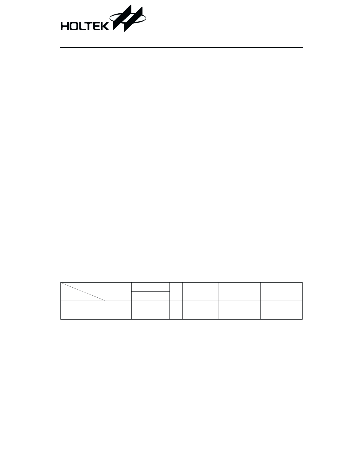
Selection Table
Function
Part No. No. Type
HT12D 8 4 L
HT12F 12 0
Notes: Data type: L stands for latch type data output.
VT can be used as a momentary data output.
Address
No.
Data
¾Ö
VT Oscillator Trigger Package
RC oscillator
Ö
RC oscillator
1 July 12, 1999
DIN active ²Hi²
DIN active ²Hi²
18 DIP/20 SOP
18 DIP/20 SOP
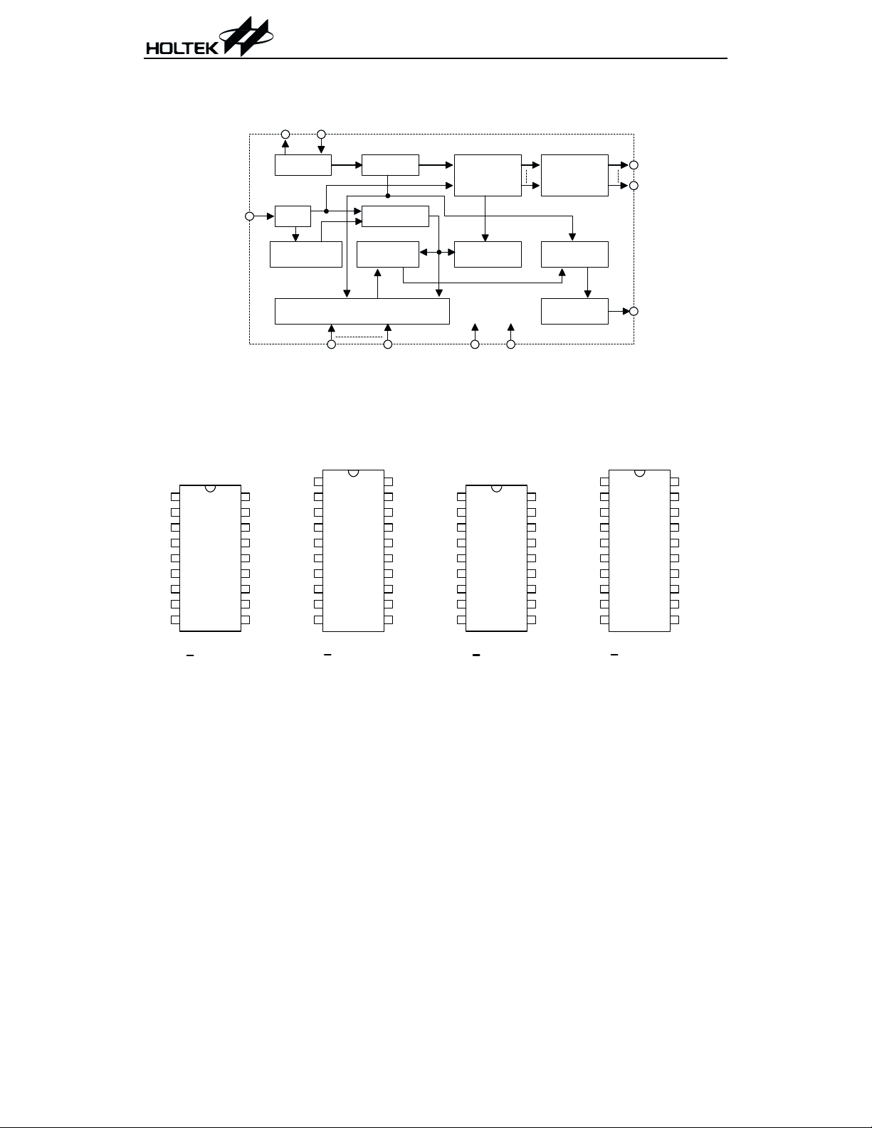
Block Diagram
212Series of Decoders
OSC1OSC2
D ivider
D a ta D e te c to r
C om parator C om parator
Address
D ata Shift
R egister
VDD VSS
Latch C ircuit
C ontrol Logic
Buffer T ra n s m is s io n G a te C irc u it
Data
VT
DIN
O scillator
Buffer
S y n c . D e te c to r
Note: The address/data pins are available in various combinations (see the address/data table).
Pin Assignment
VDD
VT
OSC1
OSC2
DIN
A11
A10
A9
A8
12-A ddress
0 -D a ta
NC
1
A0
2
A1
3
A2
4
A3
5
A4
6
A5
7
A6
8
A7
9
VSS
10
HT12F
2 0 S O P
20
NC
19
VDD
18
VT
17
OSC1
16
OSC2
15
DIN
14
A11
13
A10
12
A9
11
A8
8-A ddress
4-D ata
1
A0
2
A1
3
A2
4
A3
5
A4
6
A5
7
A6
8
A7
9
VSS
H T12D
18 D IP
8-A ddress
4-D ata
NC
18
VDD
17
VT
16
OSC1
15
OSC2
14
DIN
13
D11
12
D10
11
D9
10
D8
A0
A1
A2
A3
A4
A5
A6
A7
VSS
1
2
3
4
5
6
7
8
9
10
20
NC
19
VDD
18
VT
17
OSC1
16
OSC2
15
DIN
14
D11
13
D10
12
D9
11
D8
HT12D
2 0 S O P
12-A ddress
0 -D a ta
1
A0
2
A1
3
A2
4
A3
5
A4
6
A5
7
A6
8
A7
9
VSS
H T12F
18 D IP
18
17
16
15
14
13
12
11
10
2 July 12, 1999
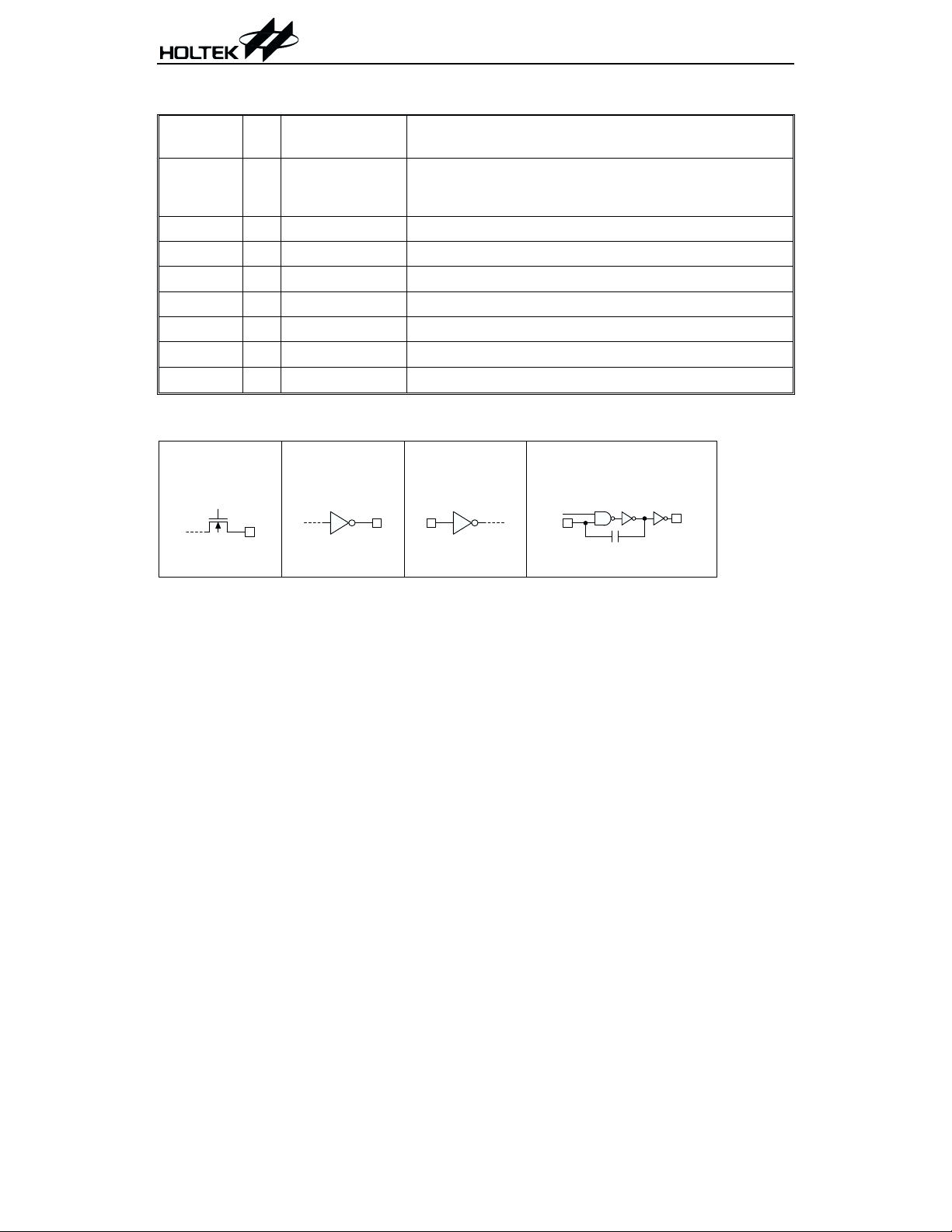
Pin Description
212Series of Decoders
Pin Name I/O
A0~A11 I
Internal
Connection
NMOS
TRANSMISSION
GATE
Description
Input pins for address A0~A11 setting
They can be externally set to VDD or VSS.
D8~D11 O CMOS OUT Output data pins
DIN I CMOS IN Serial data input pin
VT O CMOS OUT Valid transmission, active high
OSC1 I OSCILLATOR Oscillator input pin
OSC2 O OSCILLATOR Oscillator output pin
VSS I
VDD I
¾
¾
Negative power supply (GND)
Positive power supply
Approximate internal connection circuits
NMOS
TRANSM ISSION
GATE
CMOS OUT
C M O S IN
EN
OSC1
O S C ILLA TO R
OSC2
Absolute Maximum Ratings
Supply Voltage...............................-0.3V to 13V
Input Voltage....................V
-0.3 to VDD+0.3V
SS
Note: These are stress ratings only. Stresses exceeding the range specified under ²Absolute Maxi
mum Ratings² may cause substantial damage to the device. Functional operation of this de
vice at other conditions beyond those listed in the specification is not implied and prolonged
exposure to extreme conditions may affect device reliability.
Storage Temperature.................-50°Cto125°C
Operating Temperature ..............-20°Cto75°C
3 July 12, 1999
-
-

212Series of Decoders
Electrical Characteristics
Symbol Parameter
V
I
I
I
I
V
V
f
DD
STB
DD
O
VT
IH
IL
OSC
Operating Voltage
Standby Current
Operating Current 5V
Data Output Source
Current (D8~D11)
Data Output Sink
Current (D8~D11)
VT Output Source Current
VT Output Sink Current
²H² Input Voltage
²L² Input Voltage
Oscillator Frequency 5V
Test Conditions
V
DD
Conditions
¾¾
5V
Oscillator stops
12V
No load
f
=150kHz
OSC
=4.5V
V
5V
5V
5V
5V
5V
OH
V
=0.5V
OL
=4.5V
V
OH
V
=0.5V
OL
¾
¾
=51kW¾
R
OSC
Ta=25°C
Min. Typ. Max. Unit
2.4 5 12 V
¾
¾
¾
-1 -1.6 ¾
1 1.6
-1 -1.6 ¾
1 1.6
3.5
0
0.1 1
24
200 400
¾
¾
¾
¾
150
5V
1V
¾
mA
mA
mA
mA
mA
mA
mA
kHz
4 July 12, 1999

Functional Description
212Series of Decoders
Operation
12
The 2
binations of addresses and data pins in differ
ent packages so as to pair with the 2
series of decoders provides various com
12
series of
encoders.
The decoders receive data that are transmitted
by an encoder and interpret the first N bits of
code period as addresses and the last 12-N bits
as data, where N is the address code number. A
signal on the DIN pin activates the oscillator
which in turn decodes the incoming address
and data. The decoders will then check the re
ceived address three times continuously. If the
received address codes all match the contents of
the decoder¢s local address, the 12-N bits of
data are decoded to activate the output pins
and the VT pin is set high to indicate a valid
transmission. This will last unless the address
code is incorrect or no signal is received.
The output of the VT pin is high only when the
transmission is valid. Otherwise it is always
low.
Output type
Of the 2
12
series of decoders, the HT12F has no
data output pin but its VT pin can be used as a
momentary data output. The HT12D, on the
other hand, provides 4 latch type data pins
whose data remain unchanged until new data
are received.
Part
Data
No.
Pins
Address
Pins
Output
Type
Operating
Voltage
Flowchart
The oscillator is disabled in the standby state
-
-
and activated when a logic ²high² signal applies
to the DIN pin. That is to say, the DIN should be
kept low if there is no signal input.
Power on
Standby m ode
-
No
No
C ode in ?
Yes
Address bits
m atched ?
Yes
Store data
Match
previous stored
data ?
Yes
3 tim es
of checking
com pleted ?
Yes
Latch data
to o u tp u t &
a c tiv a te V T
D isable VT &
ignore the rest of
No
No
th is w o r d
HT12D 4 8 Latch 2.4V~12V
HT12F 0 12
¾
2.4V~12V
No
5 July 12, 1999
Address or
data error ?
Yes

Decoder timing
Encoder
Transm ission
Enable
Encoder
DOUT
D ecoder V T
Latched
Data O ut
< 1 word
4 w ords
check
Encoder/Decoder cross reference table
Decoders
Part No.
Data Pins Address Pins VT Pair Encoder
HT12D 4 8
HT12F 0 12
14
2 c lo c k s
Transm itted
C ontinuously
check
HT12A 18 20
Ö
HT12E 18 20
HT12A 18 20
Ö
HT12E 18 20
212Series of Decoders
4 w ords
Encoder Decoder
DIP SOP DIP SOP
14
2 clocks
Package
18 20
18 20
Address/Data sequence
The following table provides address/data sequence for various models of the 2
12
series of decoders. A
correct device should be chosen according to the requirements of the individual addresses and data.
Address/Data Bits
Part No.
0 1 2 3 4 5 6 7 8 9 10 11
HT12D A0 A1 A2 A3 A4 A5 A6 A7 D8 D9 D10 D11
HT12F A0 A1 A2 A3 A4 A5 A6 A7 A8 A9 A10 A11
6 July 12, 1999

Oscillator frequency vs supply voltage
fo s c
(S cale)
4.00
3.50
212Series of Decoders
Rosc (9)
27k
30k
3.00
2 .5 0
2 .0 0
1.50
(100kH z)1.00
0.50
0.25
234 567 8910111213VDD (V DC)
The recommended oscillator frequency is f
(decoder) @ 50 f
OSCD
33k
36k
39k
43k
47k
51k
56k
62k
68k
75k
82k
100k
120k
150k
180k
220k
(HT12E encoder)
OSCE
1
@
3
(HT12A encoder).
f
OSCE
7 July 12, 1999

Application Circuits
212Series of Decoders
Receiver Circuit
1
A0
2
A1
3
4
5
6
7
8
9
A2
A3
A4
A5
A6
A7
VSS
OSC1
OSC2
H T12D
VDD
VT
DIN
D11
D10
D9
D8
18
17
16
15
14
13
12
11
10
R
VDD
OSC
R e c e iv e r C irc u it
1
A0
2
A1
3
A2
4
A3
5
A4
6
A5
7
A6
8
A7
9
VSS
H T12F
VDD
VT
OSC1
OSC2
DIN
A11
A10
A9
A8
18
17
16
15
14
13
12
11
10
R
Notes: Typical infrared receiver: PIC-12043T/PIC-12043S (KODESHI CORP.)
or LTM9052 (LITEON CORP.)
Typical RF receiver: JR-200 (JUWA CORP.)
RE-99 (MING MICROSYSTEM, U.S.A.)
VDD
OSC
8 July 12, 1999

212Series of Decoders
Holtek Semiconductor Inc. (Headquarters)
No.3 Creation Rd. II, Science-based Industrial Park, Hsinchu, Taiwan, R.O.C.
Tel: 886-3-563-1999
Fax: 886-3-563-1189
Holtek Semiconductor Inc. (Taipei Office)
5F, No.576, Sec.7 Chung Hsiao E. Rd., Taipei, Taiwan, R.O.C.
Tel: 886-2-2782-9635
Fax: 886-2-2782-9636
Fax: 886-2-2782-7128 (International sales hotline)
Holtek Microelectronics Enterprises Ltd.
RM.711, Tower 2, Cheung Sha Wan Plaza, 833 Cheung Sha Wan Rd., Kowloon, Hong Kong
Tel: 852-2-745-8288
Fax: 852-2-742-8657
Copyright ã 1999 by HOLTEK SEMICONDUCTOR INC.
The information appearing in this Data Sheet is believed to be accurate at the time of publication. However, Holtek
assumes no responsibility arising from the use of thespecifications described. The applications mentioned herein are
used solely for the purpose of illustration and Holtek makes no warranty or representation that such applications
will be suitable without further modification, nor recommends the use of its products for application that may pres
ent a risk to human life due to malfunction or otherwise. Holtek reserves the right to alter its products without prior
notification. For the most up-to-date information, please visit our web site at http://www.holtek.com.tw.
9 July 12, 1999
-
 Loading...