Features
•
Low power consumption
•
Low voltage dropout
•
Low temperature coefficient
Applications
•
Battery-powered equipment
•
Communication equipment
General Description
The HT10XX series is a set of three-terminal low
power voltage regulators implemented in CMOS
technology. They are available with several fixed
output voltages ranging from 1.5V~7.0V. The advantage of CMOS technology is low voltage dropout and low quiescent current.
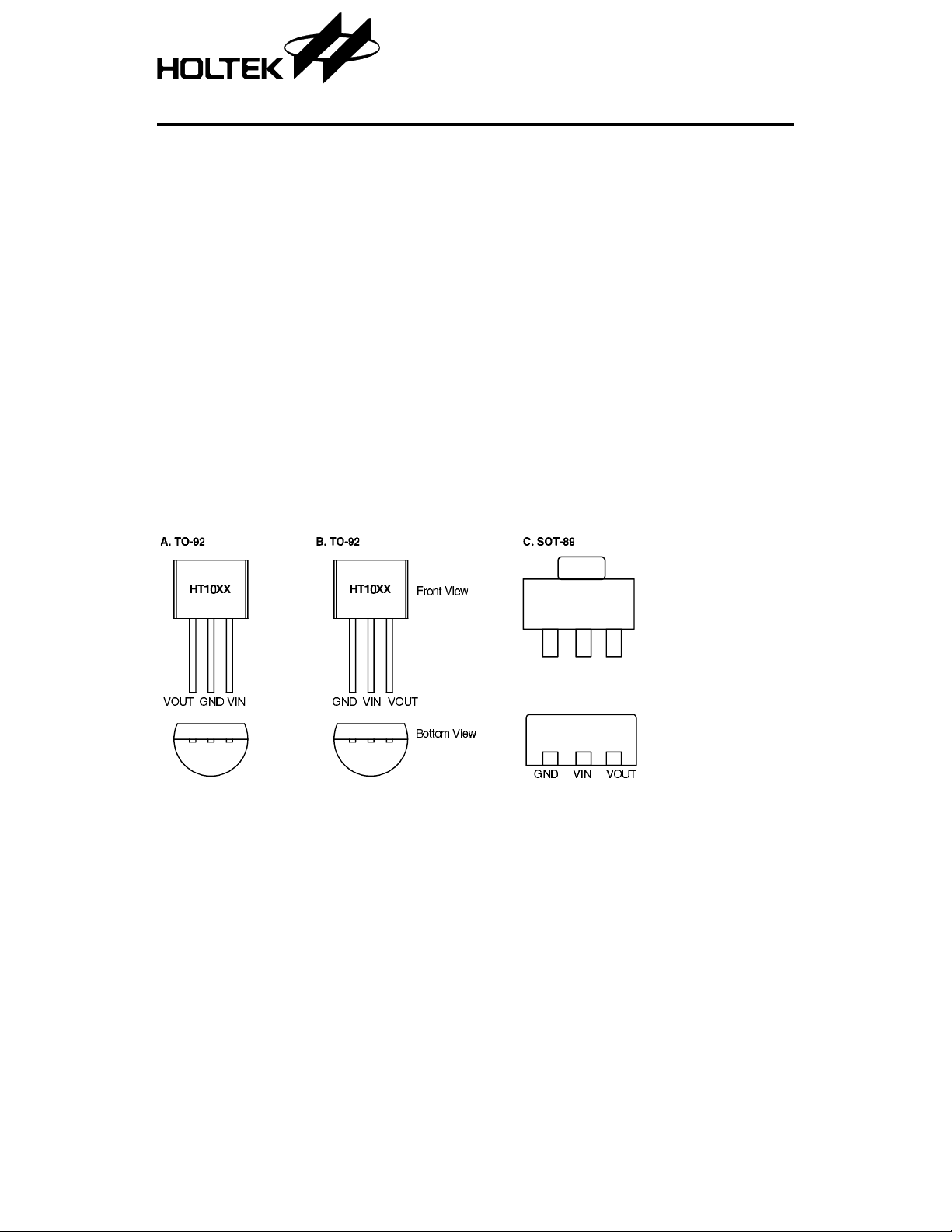
Pin Assignment
HT10XX
Voltage Regulator
•
Wide operating voltage (12V Max.)
•
TO-92 & SOT-89 packages
•
Audio/Video equipment
Although designed primarily as fixed voltage
regulators, these devices can be used with external compone nts to obtain variable voltages
and currents.
1 3rd Oct ’96

HT10XX
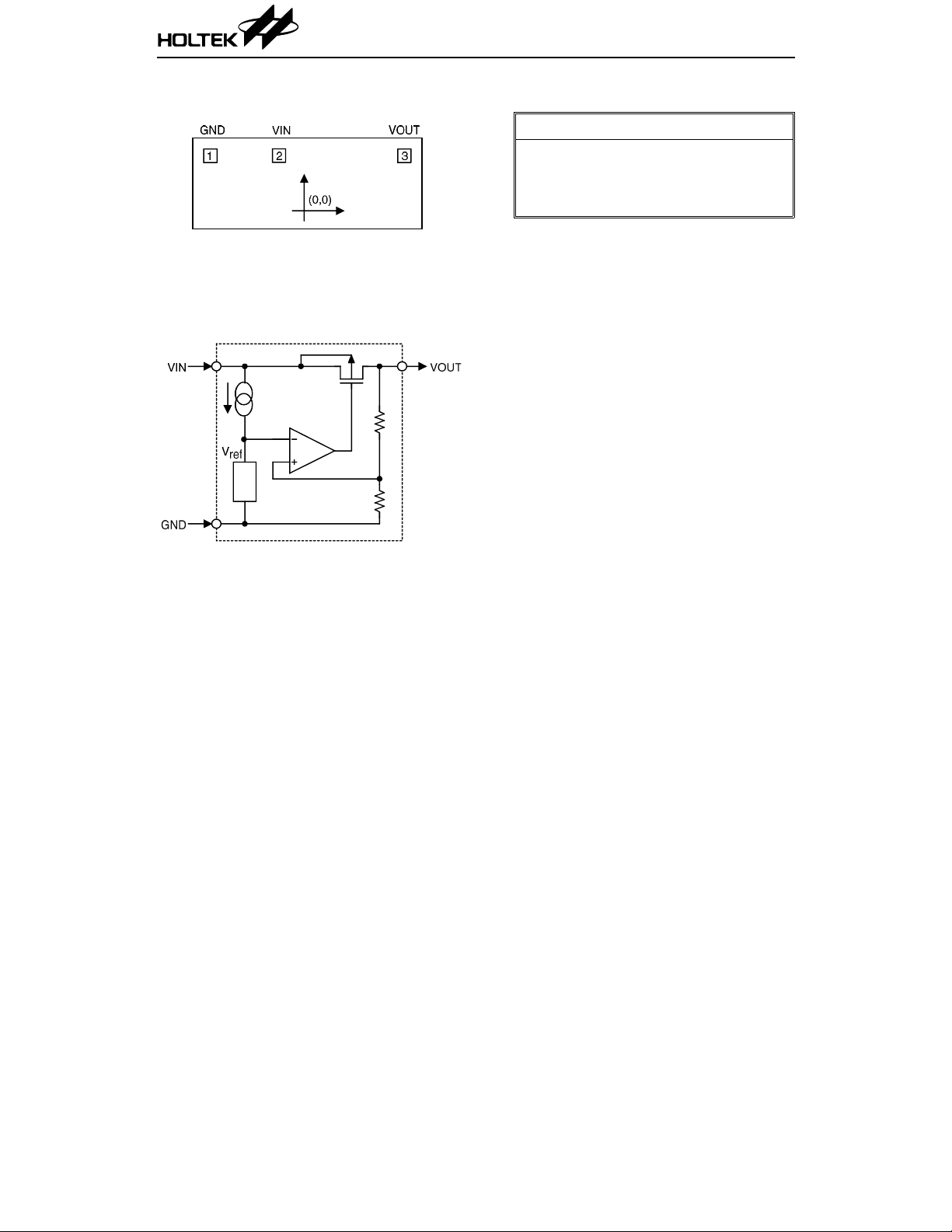
Pad Assignment Unit:mil
Pad No. X Y
1 –28.2 16.6
2 –7.55 16.7
3 –30.1 16.6
Chip size: 76
*The IC substrate should be connected to VDD in the PCB layout artwork.
× 50 (mil)
2
Block Diagram
Absolu te Maximum Ra tin g s
Supply Voltage ...............................–0.3V to 13 V Storage Temperature.................–50°C to 125°C
Power Dissipation...................................250mW Operating Temperature................... 0
°C to 70°C
2 3rd Oct ’96

HT10XX
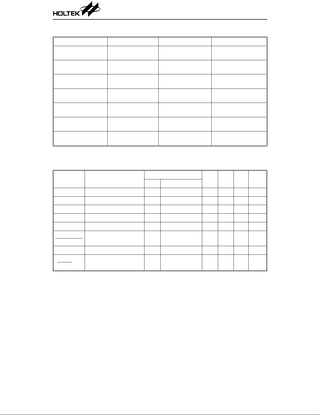
Selection Guide
Item Pin Assignment Output Voltage T olerance
HT1015
HT1016
HT1030
HT1031
HT1033
HT1034
HT1036
HT1037
HT1044
HT1045
HT1050
HT1051
HT1070
HT1071
Electrical Characteristics
HT10XX series (HT1 01 5, HT10 16 , +1.5V outpu t type) (Ta=25°C)
B
A
B
A
B
A
B
A
B
A
B
A
B
A
1.5V
3.0V
3.3V
3.6V
4.4V
5.0V
7.0V
±2.4%, ±5%
±2.4%, ±5%
±2.4%, ±5%
±2.4%, ±5%
±2.4%, ±5%
±2.4%, ±5%
±2.4%, ±5%
Symbol Parameter
V
OUT
I
OUT
∆V
V
DIF
I
SS
∆V
∆V
IN
V
IN
∆V
∆T
OUT
OUT
• V
OUT
a
Output Voltage Tolerance 3.5V I
Output Current 3.5V — 7.0 — — mA
Load Regulation 3.5V 1mA≤I
Voltage Dropout — I
Current Consumption 3.5V No load — 2.2 5.0 µA
Line Regulation —
OUT
Input Voltage — — — — 12 V
Temperature Coefficient 3.5V
Test Condition
V
IN
Condition
=0.5mA 1.425 1.5 1.575 V
OUT
≤7mA—80—mV
OUT
=0.5mA — 300 — mV
OUT
≤VIN≤12V
2.5V
I
=0.5mA
OUT
=0.5mA
I
OUT
0°C<Ta<70°C
3 3rd Oct ’96
Min. Typ. Max. Unit
— 0.2 — %/V
—
±0.25 — mV/°C

HT10XX
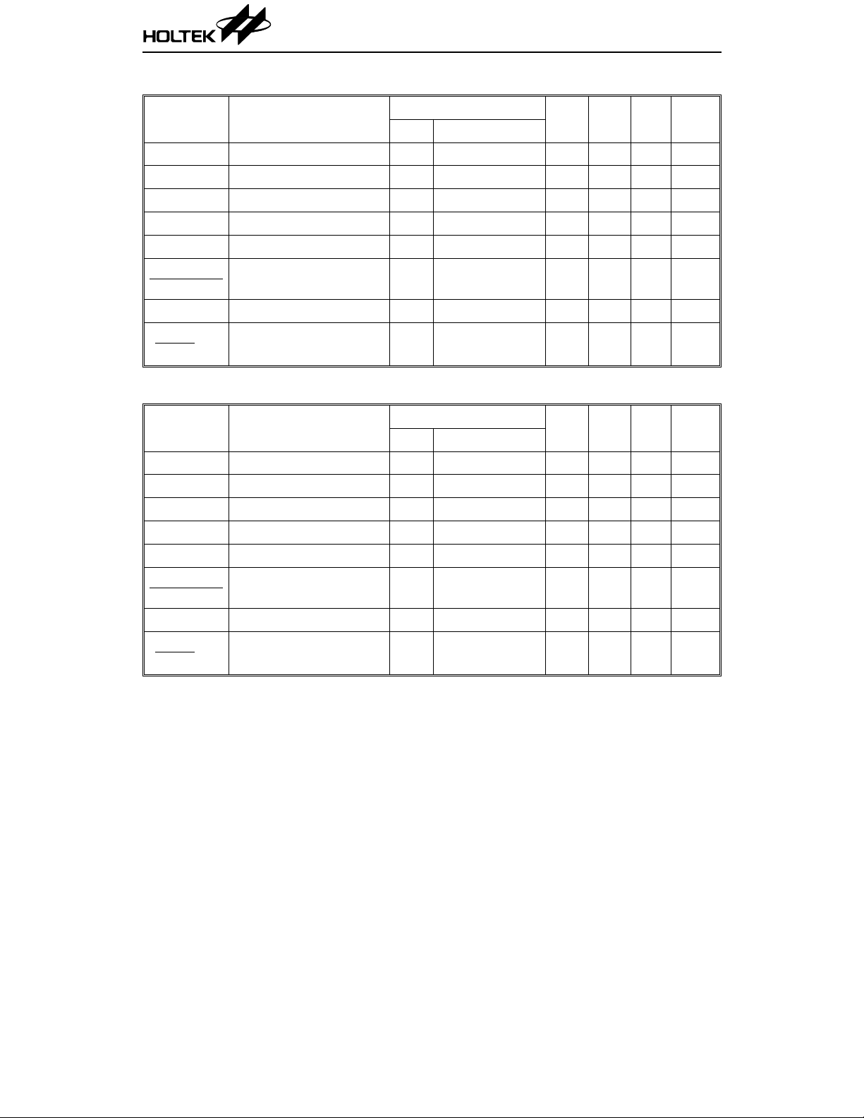
HT10XX series (HT1 03 0, HT10 31 , +3.0V outpu t type) (Ta=25°C)
Symbol Parameter
V
I
∆V
V
I
∆V
V
∆V
OUT
OUT
DIF
SS
∆V
IN
IN
∆T
OUT
OUT
• V
OUT
a
Output Voltage Tolerance 5V I
Output Current 5V — 20 30 — mA
Load Regulation 5V 1mA≤I
Voltage Dropout — I
Current Consumption 5V No load — 2.5 6.0 µA
Line Regulation —
OUT
Input Voltage — — — — 12 V
Temperature Coefficient 5V
Test Condition
V
IN
Condition
=10mA 2.85 3.0 3.15 V
OUT
=1mA — 60 — mV
OUT
≤VIN≤12V
4V
I
=1mA
OUT
=10mA
I
OUT
0°C<Ta<70°C
Min. Typ. Max. Unit
≤20mA — 60 100 mV
OUT
— 0.2 — %/V
—
±0.45 — mV/°C
HT10XX series (HT1 03 3, HT10 34 , +3.3V outpu t type) (Ta=25°C)
Symbol Parameter
V
I
∆V
V
I
∆V
V
∆V
OUT
OUT
DIF
SS
∆V
IN
IN
∆T
OUT
OUT
• V
OUT
a
Output Voltage Tolerance 5.5V I
Output Current 5.5V — 20 30 — mA
Load Regulation 5.5V 1mA≤I
Voltage Dropout — I
Current Consumption 5.5V No load — 2.5 6.0 µA
Line Regulation —
OUT
Input Voltage — — — — 12 V
Temperature Coefficient 5.5V
Test Condition
V
IN
Condition
=10mA 3.135 3.3 3.465 V
OUT
=1mA — 60 — mV
OUT
≤VIN≤12V
4.5V
I
=1mA
OUT
=10mA
I
OUT
0°C<Ta<70°C
Min. Typ. Max. Unit
≤30mA — 60 100 mV
OUT
— 0.2 — %/V
—
±0.5 — mV/°C
4 3rd Oct ’96

HT10XX
HT10XX series (HT1 03 6, HT10 37 , +3.6V outpu t type) (Ta=25°C)
Symbol Parameter
V
OUT
I
OUT
∆V
V
IDF
I
SS
∆V
∆V
IN
V
IN
∆V
∆T
OUT
OUT
• V
OUT
a
Output Voltage Tolerance 5.6V I
Output Current 5.6V — 20 30 — mA
Load Regulation 5.6V 1mA≤I
Voltage Dropout — I
Current Consumption 5.6V No load — 3.0 7.0 µA
Line Regulation —
OUT
Input Voltage — — — — 12 V
Temperature Coefficient 5.6V
Test Condition
V
IN
Condition
=10mA 3.42 3.6 3.78 V
OUT
=1mA —60—mV
OUT
≤VIN≤12V
4.6V
I
=1mA
OUT
=10mA
I
OUT
0°C<Ta<70°C
Min. Typ. Max. Unit
≤30mA — 60 100 mV
OUT
— 0.2 — %/V
—
±0.6 — mV/°C
HT10XX series (HT1 04 4, HT10 45 , +4.4V outpu t type) (Ta=25°C)
Symbol Parameter
V
OUT
I
OUT
∆V
V
DIF
I
SS
∆V
∆V
IN
V
IN
∆V
∆T
OUT
OUT
• V
OUT
a
Output Voltage Tolerance 6.4V I
Output Current 6.4V — 20 30 — mA
Load Regulation 6.4V 1mA≤I
Voltage Dropout — I
Current Consumption 6.4V No load — 3.0 7.5 µA
Line Regulation —
OUT
Input Voltage — — — — 12 V
Temperature Coefficient 6.4V
Test Condition
V
IN
Condition
=10mA 4.18 4.4 4.62 V
OUT
=1mA —60—mV
OUT
≤VIN≤12V
5.4V
I
=1mA
OUT
=10mA
I
OUT
0°C<Ta<70°C
Min. Typ. Max. Unit
≤30mA — 60 100 mV
OUT
— 0.2 — %/V
—
±0.7 — mV/°C
5 3rd Oct ’96
 Loading...