

CMOS 2K 3-Wire Serial EEPROM
Features
·
Operating voltage: 2.2V~5.5V
·
Low power consumption
-
Operating: 5mA max.
-
Standby: 10mA max.
·
User selectable internal organization
-
2K(HT93LC56): 256´8or128´16
·
3-wire Serial Interface
·
Write cycle time: 5ms max.
General Description
The HT93LC56 is a 2K-bit low voltage nonvolatile, serial
electrically erasable programmable read only memory
device using the CMOS floating gate process. Its 2048
bits of memory are organized into 128 words of 16 bits
each when the ORG pin is connected to VCC or orga
nized into 256 words of 8 bits each when it is tied to
HT93LC56
·
Automatic erase-before-write operation
·
Word/chip erase and write operation
·
Write operation with built-in timer
·
Software controlled write protection
·
10-year data retention after 100K rewrite cycles
·
106rewrite cycles per word
·
Commercial temperature range (0°Cto+70°C)
·
8-pin DIP/SOP/TSSOP package
VSS. The device is optimized for use in many industrial
and commercial applications where low power and low
voltage operation are essential. By popular
microcontroller, the versatile serial interface including
chip select (CS), serial clock (SK), data input (DI) and
data output (DO) can be easily controlled.
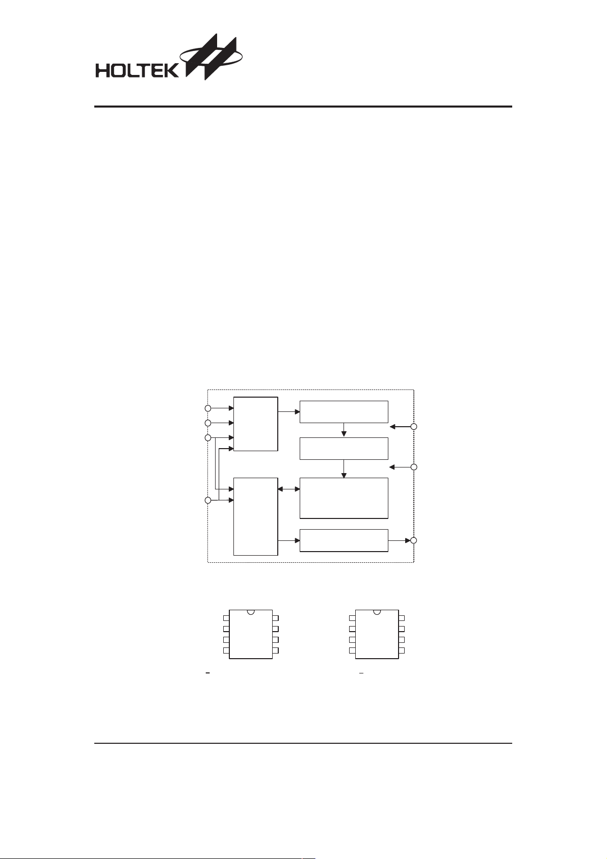
Block Diagram
Pin Assignment
C S
S K
O R G
D I
C S
1
S K
2
3
D I
4
D O
H T 9 3 L C 5 6
8 D I P - A / S O P - A / T S S O P - A
C o n t r o l
L o g i c
a n d
C l o c k
G e n e r a t o r
D a t a
R e g i s t e r
A d d r e s s
R e g i s t e r
V C C
A d d r e s s
D e c o d e r
V S S
M e m o r y C e l l
A r r a y
2 K : ( 2 5 6
V C C
8
N C
7
6
O R G
5
V S S
8 o r 1 2 8 ´ 1 6 )
´
O u t p u t
B u f f e r
N C
1
V C C
2
3
C S
4
S K
H T 9 3 L C 5 6
8 S O P - B
D O
O R G
8
V S S
7
6
D O
5
D I
Rev. 1.30 1 March 15, 2006
HT93LC56
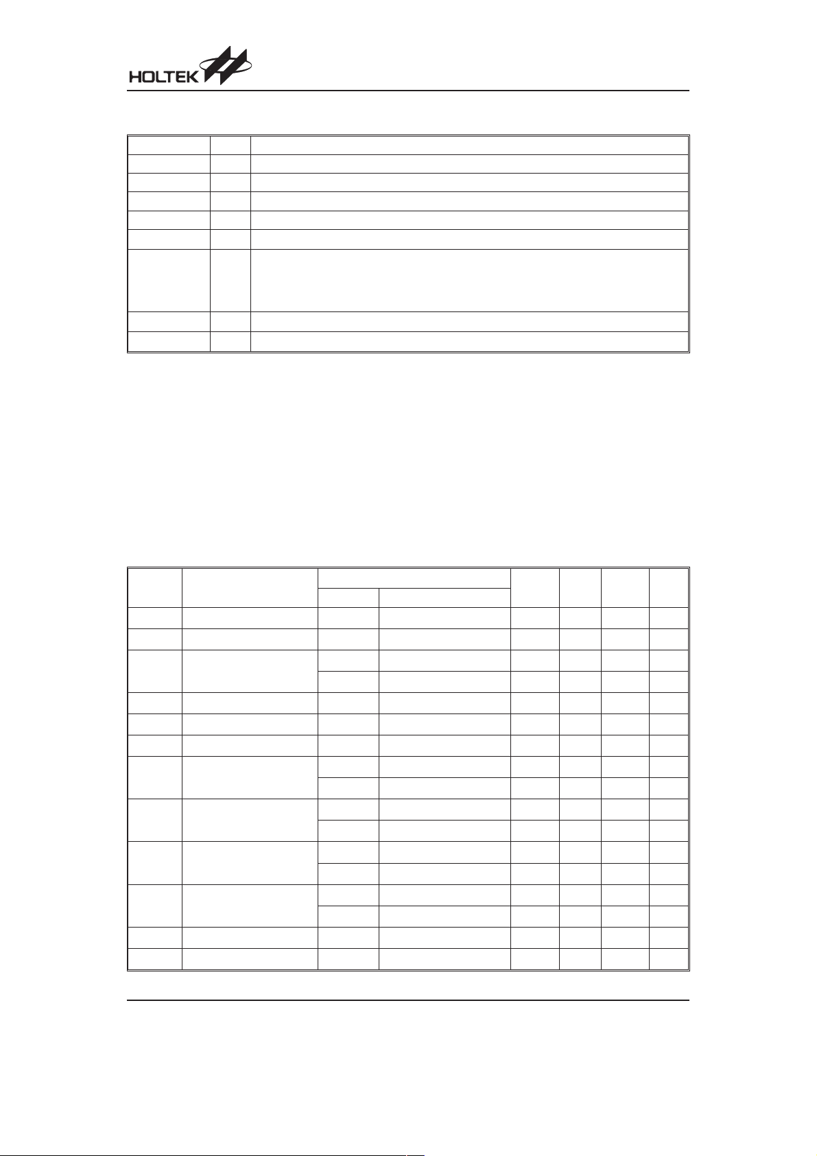
Pin Description
Pin Name I/O Description
CS I Chip select input
SK I Serial clock input
DI I Serial data input
DO O Serial data output
VSS
ORG I
NC
VCC
Absolute Maximum Ratings
Operation Temperature (Commercial)..........................................................................................................0°Cto70°C
Applied V
Applied Voltage onany Pin with Respect to VSS
Note: These are stress ratings only. Stresses exceeding the range specified under ²Absolute Maximum Ratings² may
Voltage with Respectto VSS ...................................................................................VSS-0.3V toVSS+6.0V
CC
cause substantial damage to the device. Functional operation of this device at other conditions beyond those
listed in the specification is not implied and prolonged exposure to extreme conditions may affect device reliability.
Negative power supply, ground
¾
Internal Organization
When ORG is connected to VDD or ORG is floated, the (´16) memory organization is se
lected. When ORG is tied to VSS, the (´8) memory organization is selected. There is an in
ternal pull-up resistor on the ORG pin. (HT93LC56-A)
No connection
¾
Positive power supply
¾
..................................................................................................VSS
-0.3V toVCC+0.3V
-
-
D.C. Characteristics
Symbol Parameter
V
I
I
I
I
I
V
V
V
V
C
C
CC1
CC2
STB
LI
LO
Operating Voltage
CC
Operating Current (TTL) 5V DO unload, SK=1MHz
Operating Current
(CMOS)
Standby Current (CMOS) 5V CS=SK=DI=0V
Input Leakage Current 5V
Output Leakage Current 5V
Input Low Voltage
IL
IH
OL
OH
IN
OUT
Input High Voltage
Output Low Voltage
Output High Voltage
Input Capacitance
Output Capacitance
Test Conditions
V
CC
Conditions
¾¾
5V DO unload, SK=1MHz
2.2V~5.5V DO unload, SK=250kHz
V
IN=VSS~VCC
, CS=0V
¾
¾
¾
¾
5V
2.2V~5.5V
5V
2.2V~5.5V
5V
2.2V~5.5V
5V
2.2V~5.5V
¾
¾
V
OUT=VSS~VCC
=2.1mA
I
OL
=10mA ¾¾
I
OL
=-400mA
I
OH
I
=-10mAV
OH
=0V, f=250kHz
V
IN
=0V, f=250kHz
V
OUT
Min. Typ. Max. Unit
2.2
¾
¾¾
¾¾
¾¾
¾¾
0
0
0
0
2
0.9V
CC
¾
¾
¾
¾
¾
¾
¾¾
5.5 V
5mA
5mA
5mA
10
1
1
0.8 V
0.1V
CC
V
CC
V
CC
0.4 V
0.2 V
2.4
CC
¾¾
¾¾
¾¾
-0.2 ¾¾
5pF
5pF
mA
mA
mA
V
V
V
V
V
Rev. 1.30 2 March 15, 2006
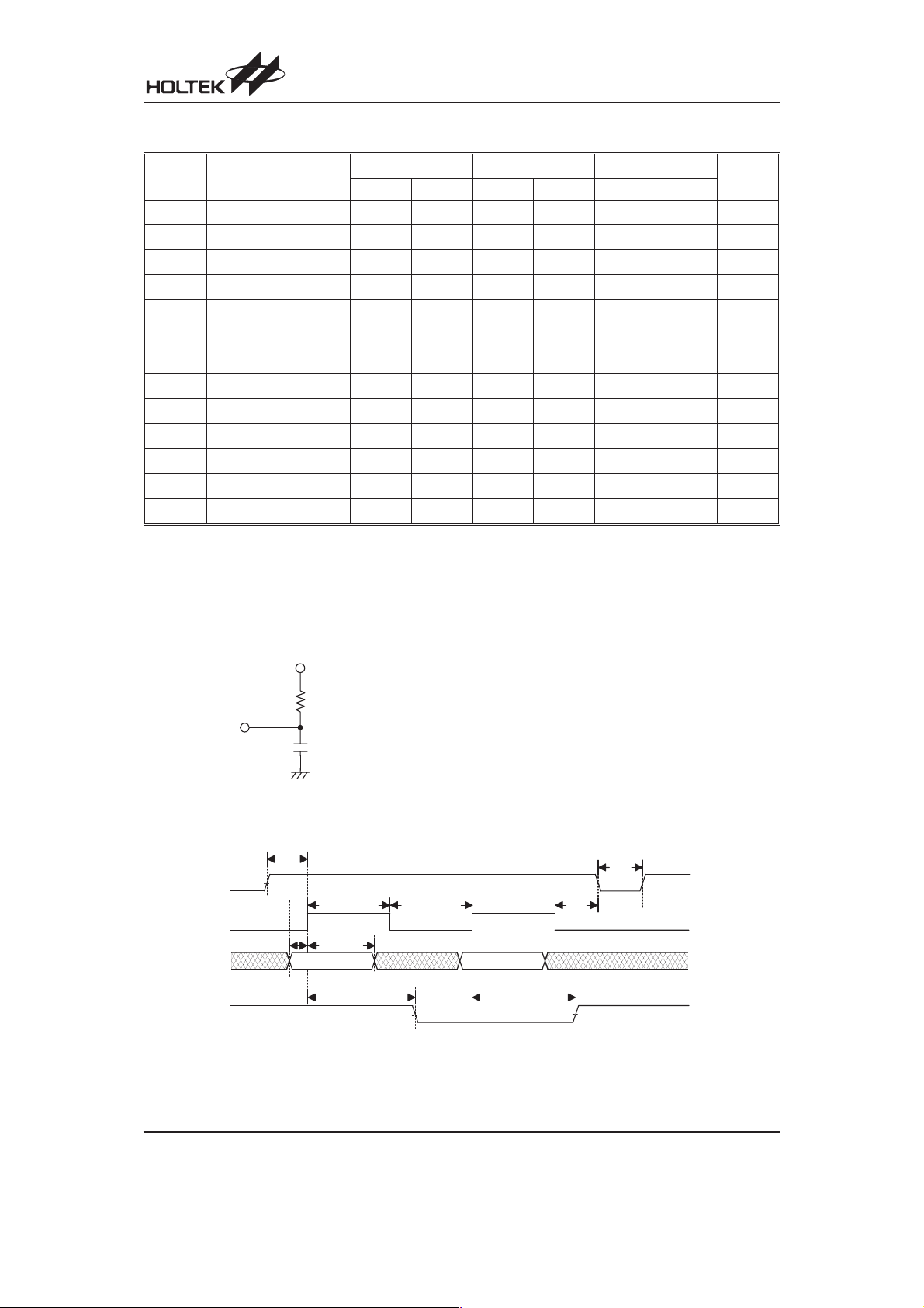
A.C. Characteristics
Symbol Parameter
f
t
t
t
t
t
t
t
t
t
t
t
t
SK
SKH
SKL
CSS
CSH
CDS
DIS
DIH
PD1
PD0
SV
HV
PR
Clock Frequency 0 2000 0 500 0 250 kHz
SK High Time 250
SK Low Time 250
CS Setup Time 50
CS Hold Time 0
CS Deselect Time 250
DI Setup Time 100
DI Hold Time 100
DO Delay to ²1²¾
DO Delay to ²0²¾
Status Valid Time
DO Disable Time 100
Write Cycle Time
VCC=5V±10% VCC=3V±10%
VCC=2.2V
Min. Max. Min. Max. Min. Max.
¾
¾
¾
¾
¾
¾
¾
250
250
¾
250
¾
¾
5
1000
1000
200
0
250
200
200
¾
¾
¾
400
¾
¾
¾
¾
¾
¾
¾
¾
1000
1000
250
¾
5
2000
2000
200
0
1000
400
400
¾
¾
¾
¾
¾
¾
¾
¾
¾
2000 ns
2000 ns
¾¾
400
¾
¾¾
HT93LC56
Unit
ns
ns
ns
ns
ns
ns
ns
ns
ns
ms
A.C. Test Conditions
Input rise and fall time: 5ns (1V to 2V)
Input and output timing reference levels: 1.5V
Output load circuit: See Figure below.
V C C = 1 . 9 5 2 V
8 0 0
W
D O
1 0 0 p F *
* Including Scope and Jig
t
C S
S K
D I
D O
C S S
t
D I S
H i - Z
t
t
D I H
V a l i d D a t a
S K H
t
P D 0
t
C D S
t
S K L
V a l i d D a t a
t
P D 1
t
C S H
Rev. 1.30 3 March 15, 2006

Functional Description
The HT93LC56 is accessed via a three-wire serial com
munication interface. The device is arranged into 128
words by 16 bits or 256 words by 8 bits depending whether
the ORG pin is connected to VCC or VSS. The HT93LC56
contains seven instructions: READ, ERASE, WRITE,
EWEN, EWDS, ERAL and WRAL. When the user
selectable internal organization is arranged into
128´16 (256´8), these instructions are all made up of
11(12) bits data: 1 start bit, 2 op code bits and 8(9) address
bits.
By using the control signal CS, SK and data input signal
DI, these instructions can be given to the HT93LC56.
These serial instruction data presented at the DI input
will be written into the device at the rising edge of SK.
During the READ cycle, DO pin acts as the data output
and during the WRITE or ERASE cycle, DO pin indi
cates the BUSY/READY status. When the DO pin is ac
tive for read data or as a BUSY/READY indicator the CS
pin must be high; otherwise DO pin will be in a
high-impedance state. For successful instructions, CS
must be low once after the instruction is sent. After
power on, the device is by default in the EWDS state.
And, an EWEN instruction must be performed before
any ERASE or WRITE instruction can be executed. The
following are the functional descriptions and timing diagrams of all seven instructions.
READ
The READ instruction will stream out data at a specified
address on the DO pin. The data on DO pin changes
during the low-to-high edge of SK signal. The 8 bits or
16 bits data stream is preceded by a logical ²0² dummy
bit. Irrespective of the condition of the EWEN or EWDS
instruction, the READ command is always valid and in
dependent of these two instructions. After the dataword
has been read the internal address will be automatically
incremented by 1 allowing the next consecutive data
word to be read out without entering further address
data. The address will wrap around with CS High until
CS returns to LOW.
HT93LC56
ERASE
-
The ERASE instruction erases data at the specified ad
dresses in the programming enable mode. After the
ERASE op-code and the specified address have been
issued, the data erase is activated by the falling edge of
CS. Since the internal auto-timing generator provides all
timing signals for the internal erase, so the SK clock is
not required. During the internal erase, we can verify the
busy/ready status if CS is high. The DO pin will remain
low butwhen the operation is over, the DO pin will return
to high and further instructions can be executed.
WRITE
The WRITE instruction writes data into the device at the
specified addresses in the programming enable mode.
After the WRITE op-code and the specified address and
data have been issued, the data writing is activated by
the falling edge of CS. Since the internal auto-timing
generator provides all timing signal for the internal writ
ing, so the SK clock is not required. The auto-timing
write cycle includes an automatic erase-before-write ca
pability. So, it is not necessary to erase data before the
WRITE instruction. During the internal writing, we can
verify the busy/ready status if CS is high. The DO pin will
remain low but when the operation is over, the DO pin
will return to high and further instructions can be executed.
ERAL
The ERALinstruction erases the entire 128´16 or 256´8
memory cellsto logical ²1² state in the programming enable mode. After the erase-all instruction set has been
issued, the data erase feature is activated by the falling
edge of CS. Since the internal auto-timing generator
provides all timing signal for the erase-all operation, so
the SK clock is not required. During the internal erase-all
operation, we can verify the busy/ready status if CS is
high. The DO pin will remain low but when the operation
is over, the DO pin will return to high and further instruc
tion can be executed.
-
-
-
-
EWEN/EWDS
The EWEN/EWDS instruction will enable or disable the
programming capabilities. At both the power on and
power off state the device automatically entered the dis
able mode. Before a WRITE, ERASE, WRAL or ERAL in
struction is given, the programming enable instruction
EWEN must be issued, otherwise the ERASE/WRITE in
struction is invalid. After the EWEN instruction is issued,
the programming enable condition remains until power is
turned off or an EWDS instruction is given. No data can be
written into the device in the programming disabled state.
By so doing, the internal memory data can be protected.
Rev. 1.30 4 March 15, 2006
WRAL
The WRAL instruction writes data into the entire 128´16
or 256´8 memory cells in the programming enable
-
mode. After the write-all instruction set has been issued,
-
the data writing is activated by the falling edge of CS.
Since the internal auto-timing generator provides all tim
-
ing signals for the write-all operation, so the SK clock is
not required. During the internal write-all operation, we
can verify the busy/ready status if CS is high. The DO
pin will remain low but when the operation is over the
DO pin will return to high and further instruction can be
executed.
-

Timing Diagrams
READ
C S
S K
D I
D O
* A d d r e s s p o i n t e r a u t o m a t i c a l l y c y c l e s t o t h e n e x t w o r d
EWEN/EWDS
( 1 )
S t a r t b i t
t
C D S
0
1
H i g h Z H i g h - Z
A N
A 0
t
0
D 0
D X
D X
H Z
*
M o d e
( X 1 6 )
A N
D X
A 6
D 1 5
HT93LC56
( X 8 )
A 7
D 7
WRITE
C S
S t a n d b y
S K
D I
( 1 )
S t a r t b i t
1 1 = E W E N
0
0
0 0 = E W D S
t
C D S
C S
v e r i f y
S t a n d b y
S K
A N - 1
D I
D O
( 1 )
S t a r t b i t
H i g h - Z
A N - 2
A N
1
0
A 1
A 0 D X
D 0
t
S V
r e a d y
b u s y
t
P R
t
H Z
Rev. 1.30 5 March 15, 2006

ERASE
ERAL
HT93LC56
t
C S
S K
A N - 1
D I
D O
( 1 )
S t a r t b i t
H i g h - Z
A N - 2
A N
1
1
A 1
A 0
C S
S K
C D S
v e r i f y
b u s y
t
P R
t
C D S
v e r i f y
S t a n d b y
t
S V
r e a d y
t
H Z
S t a n d b y
D I
( 1 )
S t a r t b i t
D O
1000
H i g h - Z
t
S V
r e a d y
b u s y
t
P R
t
H Z
WRAL
t
C D S
C S
S K
0
00
D I
D O
( 1 )
S t a r t b i t
1
H i g h - Z
D X
D 0
v e r i f y
b u s y
t
P R
S t a n d b y
t
S V
r e a d y
t
H Z
Instruction Set Summary
Instruction Comments
Start
bitOpCode
READ Read data 1 10 XA7~A0 XA6~A0 D7~D0 D15~D0
ERASE Erase data 1 11 XA7~A0 XA6~A0
WRITE Write data 1 01 XA7~A0 XA6~A0 D7~D0 D15~D0
EWEN Erase/Write Enable 1 00 11XXXXXXX 11XXXXXX
EWDS Erase/Write Disable 1 00 00XXXXXXX 00XXXXXX
ERAL Erase All 1 00 10XXXXXXX 10XXXXXX
WRAL Write All 1 00 01XXXXXXX 01XXXXXX D7~D0 D15~D0
Note: ²X² stands for ²don¢t care²
Address Data
ORG=0
X8
ORG=1
X16
ORG=0X8ORG=1
¾¾
¾¾
¾¾
¾¾
X16
Rev. 1.30 6 March 15, 2006

Package Information
8-pin DIP (300mil) Outline Dimensions
B
C
D
E
HT93LC56
A
8
5
4
1
H
G
F
a
I
Symbol
Min. Nom. Max.
A 355
B 240
C 125
D 125
E16
F50
G
¾
H 295
I 335
Dimensions in mil
¾
¾
¾
¾
¾
¾
100
¾
¾
a 0°¾15°
375
260
135
145
20
70
¾
315
375
Rev. 1.30 7 March 15, 2006

8-pin SOP (150mil) Outline Dimensions
5
8
A
1
B
4
C
HT93LC56
C '
D
E
F
Symbol
Min. Nom. Max.
A 228
B 149
C14
C¢
189
D53
E
¾
F4
G22
H4
G
H
a
Dimensions in mil
¾
¾
¾
¾
¾
50
¾
¾
¾
a 0°¾10°
244
157
20
197
69
¾
10
28
12
Rev. 1.30 8 March 15, 2006

8-pin TSSOP Outline Dimensions
HT93LC56
58
E 1
1 4
E
L 1
Dimensions in mm
¾
¾
¾
0.25
¾
¾
¾
¾
0.65
¾
¾
q
A
e
R 0 . 1 0
( 4 C O R N E R S )
Symbol
A 1.05
A1 0.05
A2 0.95
B
C 0.11
D 2.90
E 6.20
E1 4.30
e
L 0.50
L1 0.90
y
D
A 2
A 1
B
y
L
C
Min. Nom. Max.
¾
¾
¾¾
q 0°¾8°
1.20
0.15
1.05
¾
0.15
3.10
6.60
4.50
¾
0.70
1.10
0.10
Rev. 1.30 9 March 15, 2006

Product Tape and Reel Specifications
Reel Dimensions
HT93LC56
T 2
A
B
T 1
D
SOP 8N, TSSOP 8L
Symbol Description Dimensions in mm
A Reel Outer Diameter
B Reel Inner Diameter
C Spindle Hole Diameter
D Key Slit Width
T1 Space Between Flange
T2 Reel Thickness
330±1.0
62±1.5
13.0+0.5
2.0±0.5
12.8+0.3
18.2±0.2
C
-0.2
-0.2
Rev. 1.30 10 March 15, 2006

Carrier Tape Dimensions
HT93LC56
D
E
F
PD 1
P 1P 0
W
A 0
B 0
C
SOP 8N
Symbol Description Dimensions in mm
W Carrier Tape Width
P Cavity Pitch
E Perforation Position
F Cavity to Perforation (Width Direction)
D Perforation Diameter
12.0+0.3
8.0±0.1
1.75±0.1
5.5±0.1
1.55±0.1
D1 Cavity Hole Diameter 1.5+0.25
P0 Perforation Pitch
P1 Cavity to Perforation (Length Direction)
A0 Cavity Length
B0 Cavity Width
K0 Cavity Depth
t Carrier Tape Thickness
4.0±0.1
2.0±0.1
6.4±0.1
5.2±0.1
2.1±0.1
0.3±0.05
C Cover Tape Width 9.3
t
K 0
-0.1
TSSOP 8L
Symbol Description Dimensions in mm
W Carrier Tape Width
P Cavity Pitch
E Perforation Position
F Cavity to Perforation (Width Direction)
12.0+0.3
-0.1
8.0±0.1
1.75±0.1
5.5±0.5
D Perforation Diameter 1.5+0.1
D1 Cavity Hole Diameter 1.5+0.1
P0 Perforation Pitch
P1 Cavity to Perforation (Length Direction)
A0 Cavity Length
B0 Cavity Width
K0 Cavity Depth
t Carrier Tape Thickness
4.0±0.1
2.0±0.1
7.0±0.1
3.6±0.1
1.6±0.1
0.3±0.013
C Cover Tape Width 9.3
Rev. 1.30 11 March 15, 2006

Holtek Semiconductor Inc. (Headquarters)
No.3, Creation Rd. II, Science Park, Hsinchu, Taiwan
Tel: 886-3-563-1999
Fax: 886-3-563-1189
http://www.holtek.com.tw
Holtek Semiconductor Inc. (Taipei Sales Office)
4F-2, No. 3-2, YuanQu St., Nankang Software Park, Taipei 115, Taiwan
Tel: 886-2-2655-7070
Fax: 886-2-2655-7373
Fax: 886-2-2655-7383 (International sales hotline)
HT93LC56
Holtek Semiconductor Inc. (Shanghai Sales Office)
7th Floor, Building 2, No.889, Yi Shan Rd., Shanghai, China 200233
Tel: 021-6485-5560
Fax: 021-6485-0313
http://www.holtek.com.cn
Holtek Semiconductor Inc. (Shenzhen Sales Office)
5/F, Unit A, Productivity Building, Cross of Science M 3rd Road and Gaoxin M 2nd Road, Science Park, Nanshan District,
Shenzhen, China 518057
Tel: 0755-8616-9908, 8616-9308
Fax: 0755-8616-9533
Holtek Semiconductor Inc. (Beijing Sales Office)
Suite 1721, Jinyu Tower, A129 West Xuan Wu Men Street, Xicheng District, Beijing, China 100031
Tel: 010-6641-0030, 6641-7751, 6641-7752
Fax: 010-6641-0125
Holtek Semiconductor Inc. (Chengdu Sales Office)
709, Building 3, Champagne Plaza, No.97 Dongda Street, Chengdu, Sichuan, China 610016
Tel: 028-6653-6590
Fax: 028-6653-6591
Holmate Semiconductor, Inc. (North America Sales Office)
46729 Fremont Blvd., Fremont, CA 94538
Tel: 510-252-9880
Fax: 510-252-9885
http://www.holmate.com
Copyright Ó 2006 by HOLTEK SEMICONDUCTOR INC.
The information appearing in this Data Sheet is believed to be accurate at the time of publication. However, Holtek as
sumes no responsibility arising from the use of the specifications described. The applications mentioned herein are used
solely for the purpose of illustration and Holtek makes no warranty or representation that such applications will be suitable
without further modification, nor recommends the use of its products for application that may present a risk to human life
due to malfunction or otherwise. Holtek¢s products are not authorized for use as critical components in life support devices
or systems. Holtek reserves the right to alter its products without prior notification. For the most up-to-date information,
please visit our web site at http://www.holtek.com.tw.
-
Rev. 1.30 12 March 15, 2006
 Loading...