

Features
·
Operating voltage: 4.5V~5.5V
·
ADM algorithm
·
Low noise
-
Echo mode: -85dB
-
Surround mode: -90dB
Applications
·
Television
·
Karaoke systems
General Description
The HT8972 is an echo/surround effect processor. It is
designed for various audio systems including karaoke,
television, sound equipments, etc. The chip consists of
a built-in pre-amplifier, VCO or Voltage Control OSC,
40Kb SRAM, A/D and D/A converters as well as delay
time control logic.
HT8972
Voice Echo
·
Low distortion rate
-
Echo mode: 1%
-
Surround mode: 0.2%
·
Built-in 40Kb SRAM
·
Automatic reset function
·
16-pin DIP/SOP package
·
Video disc player
·
Sound equipments
Its built-in 40Kb SRAM can generate delay time effect
and can control the delay time value through the exter
nal VCO resistor.
The VCO circuit can reduce external components and
make it easy to adjust the delay time.
-
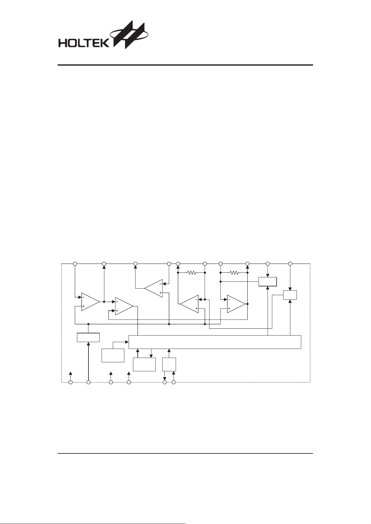
Block Diagram
L P F 1 _ I N
V C C A G N D D G N D
L P F 1 _ O U T L P F 2 _ O U T L P F 2 _ I N O P 2 _ O U T O P 2 _ I N O P 1 _ I N O P 1 _ O U T C C 0 C C 1
C O M P
L P F 1
1 / 2 V C C
A U T O
R E S E T
L P F 2
D I
M O M I C L O C K
4 0 K B i t s
R A M
V C O
O S C _ OR E F
v c o
4 . 7 k
4 . 7 k
W
W
M O D
D E M
D O 0 D O 1
Rev. 1.00 1 December 23, 2008
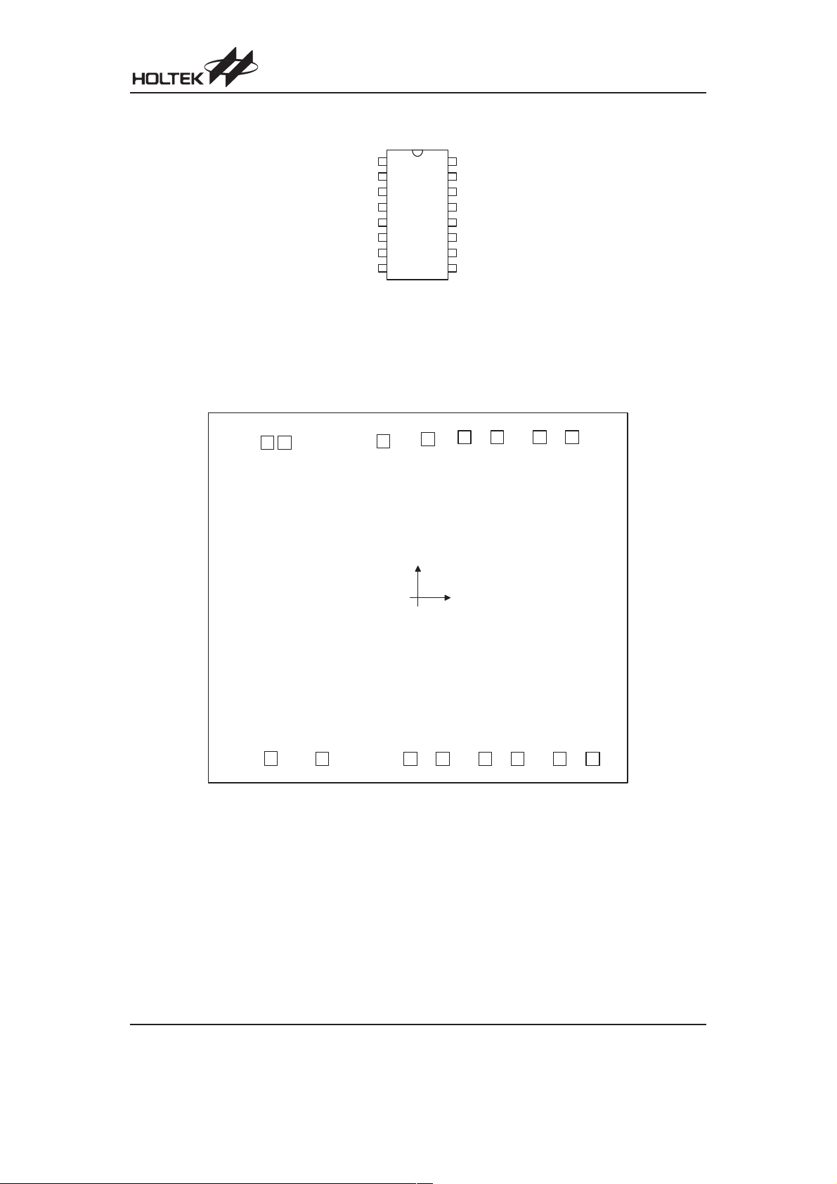
Pin Assignment
Pad Assignment
HT8972
L P F 1 _ I N
1 6
1
V C C
2
R E F
V C O
C C 1
C C 0
1 6 D I P - A / S O P - A
R E F
3
4
5
6
7
8
H T 8 9 7 2
A G N D
D G N D
O S C _ O
D G N D
A G N D
L P F 1 _ O U T
1 5
L P F 2 _ O U T
1 4
L P F 2 _ I N
1 3
O P 2 _ O U T
1 2
O P 2 _ I N
1 1
O P 1 _ I N
1 0
O P 1 _ O U T
9
L P F 1 _ O U T
L P F 1 _ I N
V C C
L P F 2 _ O U T
L P F 2 _ I N
1 6
1
2
O S C _ O
3
V C O
1 5
1 4
( 0 , 0 )
6
5
4
C C 1
C C 0
7
O P 1 _ I N
O P 1 _ O U T
1 2 1 1
1 3
1 0
8
9
O P 2 _ I N
O P 2 _ O U T
Chip size: 2475´2065 (mm)
2
* The IC substrate should be connected to VSS in the PCB layout artwork.
Rev. 1.00 2 December 23, 2008
HT8972
Pad Coordinates
Pad No. X Y Pad No. X Y
1
2
3
4
5 147.425
6 395.225
7 587.425
8 835.225
-883.875
-865.105 -891.900
-564.105 -892.700
-44.775 -892.700
861.250 9 1027.425
10 907.375 890.431
11 715.175 890.429
12 467.375 890.431
-892.700
-892.700
-892.700
-892.700
13 275.175 890.429
14 60.790 879.700
15
16
-203.150
-783.875
Pad Description
Pad No. Pad Name I/O Internal Connection Description
1 DGND I
2 OSC_O O
3 VCO I
4 CC1
5 CC0
6 OP1_OUT O
7 OP1_IN I
8 OP2_IN I
9 OP2_OUT O
10 LPF2_IN I
11 LPF2_OUT O
12 LPF1_OUT O
13 LPF1_IN I
14 VCC I
15 REF I
16 AGND I
¾
¾
¾
¾¾
¾¾
¾
¾
¾
¾
¾
¾
¾
¾
¾
¾
¾
Digital ground
System oscillator output
System oscillator input, system frequency adjustable pin
Current control 1
Current control 0
OP1 output
OP1 input
OP2 input
OP2 output
Low pass filter 2 input
Low pass filter 2 output
Low pass filter 1 output
Low pass filter 1 input
Analog and positive power supply
Analog reference voltage
Analog ground
Unit: mm
-892.700
868.440
861.250
Absolute Maximum Ratings
Supply Voltage...........................VSS-0.3V to VSS+6.0V
Input Voltage..............................V
Note: These are stress ratings only. Stresses exceeding the range specified under ²Absolute Maximum Ratings² may
cause substantial damage to the device. Functional operation of this device at other conditions beyond those listed
in the specification is not implied and prolonged exposure to extreme conditions may affect device reliability.
Rev. 1.00 3 December 23, 2008
-0.3V to VDD+0.3V
SS
Storage Temperature ............................-50°Cto125°C
Operating Temperature .............................-20°Cto70°
HT8972
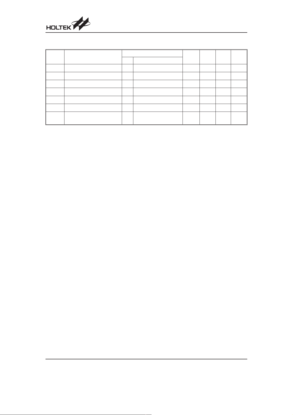
Electrical Characteristics
Symbol Parameter
V
CC
I
CC
G
V
V
OMAX
THD Total Harmonic Distortion 5V
N
O
PSRR Power Supply Rejection Ratio 5V
Operating Voltage
Operating Current 5V
Voltage Gain 5V
Maximum Output Voltage 5V THD=10% 0.9 1.8
Output Noise Voltage 5V
Test Conditions
V
DD
Conditions
¾¾
Min. Typ. Max. Unit
4.5 5.0 5.5 V
¾¾
=47kW¾-0.9
R
L
Filter= A-Weighting ¾
Filter= A-Weighting ¾-85 -60
DV
=-20dBV (0.1Vrms)
CC
f=100Hz
¾-40 -30
Ta=25°C
15 30 mA
2.5 dB
Vrms
¾
0.7 1.5 %
dBV
dB
Rev. 1.00 4 December 23, 2008

Functional Description
The HT8972 is an echo/surround effect generator with
built-in 40Kb SRAM. It ensures low distortion as well as
low noise for processing audio signal delay. The chip
provides two playing modes (echo and surround) and
the playing function block diagrams are shown as fol
lows.
·
Surround mode
V
I N
L P F 1 A / D
D e l a y
D / A L P F 2
V
O U T
HT8972
·
Echo mode
V
O U T
V
I N
L P F 1 A / D
-
D e l a y
D / A L P F 2
R
OSC-fOSC
R
f
THD
R
f
THD
R
f
THD
R
f
THD
-Delay_time-Distortion Cross table
OSC
OSC
Td
56.2 44 36.3 30.6 25.9 23.1 20.7
2 2.5 3 3.5 4 4.5 5 MHz
320 264 219 188 164 147 132 ms
1.3 1.05 0.815 0.625 0.58 0.525 0.43 %
OSC
OSC
Td
18.5 16.7 15.1 14.5 13.9 11.9 10.9
5.5 6 6.5 7 7.5 8 8.5 MHz
120 110 102 93 88 82 78 ms
0.4 0.335 0.315 0.3 0.275 0.26 0.25 %
OSC
OSC
Td
10 9 8.06 7.3 6.4 5.8 5.3
9 101112131415MHz
73.2 65.6 59.2 54.4 50 46 44 ms
0.23 0.218 0.205 0.19 0.17 0.1675 0.1575 %
OSC
OSC
Td
4.8 4.4 4 3.7 3.3 3 2.8
16 17 18 19 20 21 22 MHz
41.2 38.4 36 33.6 33 32 30 ms
0.16 0.145 0.14 0.14 0.13 0.125 0.12 %
kW
kW
kW
kW
Rev. 1.00 5 December 23, 2008

Application Circuits
Echo Mode
HT8972
1mF
1 k
W
M I C
4 . 7 k
W
V C C
V C C
F
0 . 1
m
1 0 0mF
4 7mF
R
O S C
F
0 . 1
m
2 0 k
2 0 k
W
D e l a y T i m e
0 . 1mF
1mF
4 . 7 k
W
4 . 7 k
W
1
V C C
2
R E F
3
A G N D
4
D G N D
5
O S C _ O
W
6
V C O
7
C C 1
8
C C 0
4 7 k
1 0 0mF
4 . 7 k
W
L P F 1 _ O U T
L P F 2 _ O U T
O P 2 _ O U T
O P 1 _ O U T
1 k
W
L P F 1 _ I N
L P F 2 _ I N
O P 2 _ I N
O P 1 _ I N
W
5 6 0
W
2 2mF
1 6
1 5
1 4
1 3
1 2
1 1
1 0
9
3
4 5 5 8
2
6 8 0 0 p F
1 0 k
1 0 0 0 p F
4 . 3 k
3 . 3 k
4 . 3 k
5 6 0 p F
1 0 k
4 . 3 k
6 8 0 0 p F
6 8 0 0 p F
9 V
8
1
4
4 7 k
W
3 9 p F
4 . 3 k
4 . 7mF
W
4 . 7 k
W
W
W
W
W
W
W
1 0mF
0 . 0 3 3mF
6 8 0 0 p F
M I C V O L
4 . 7mF
2 . 7 k
1 0mF
4 . 7mF
W
F e e d B a c k
5 0 k
2 0 k
E c h o M o d e
W
W
1 0 0 k
W
O u t p u t
1
2
H T 8 9 7 2
Note: 1. : Analog ground, : Digital ground
2. When the value of the Rosc increases, the range of the Delay time also increases. Please refer to the
R
OSC-fOSC
-Delay_time-Distortion Cross table for the R
& Delay time values.
OSC
Rev. 1.00 6 December 23, 2008

Surround Mode
M I C
0 . 1
HT8972
1mF
1 k
W
4 . 7 k
W
V C C
V C C
F
m
1 0 0mF
4 7mF
R
O S C
F
0 . 1
m
2 0 k
2 0 k
W
D e l a y T i m e
0 . 1mF
1mF
4 . 7 k
W
4 . 7 k
W
1
V C C
2
R E F
3
A G N D
4
D G N D
5
O S C _ O
W
6
V C O
7
C C 1
8
C C 0
4 7 k
1 0 0mF
4 . 7 k
W
L P F 1 _ O U T
L P F 2 _ O U T
O P 2 _ O U T
O P 1 _ O U T
1 k
W
L P F 1 _ I N
L P F 2 _ I N
O P 2 _ I N
O P 1 _ I N
W
5 6 0
W
2 2mF
1 6
1 5
1 4
1 3
1 2
1 1
1 0
9
3
4 5 5 8
2
6 8 0 0 p F
1 0 k
1 0 0 0 p F
4 . 3 k
4 . 3 k
5 6 0 p F
1 0 k
4 . 3 k
6 8 0 0 p F
6 8 0 0 p F
9 V
8
1
4
4 7 k
W
3 9 p F
4 . 3 k
W
W
3 . 3 k
W
W
W
W
W
6 8 0 0 p F
4 . 7mF
M I C V O L
4 . 7mF
1 0mF
2 0 k
S u r r o u n d M o d e
W
1 0 0 k
W
O u t p u t
1
2
H T 8 9 7 2
Note: 1. : Analog ground, : Digital ground
2. When the value of the Rosc increases, the range of the Delay time also increases. Please refer to the
R
OSC-fOSC
-Delay_time-Distortion Cross table for the R
& Delay time values.
OSC
Rev. 1.00 7 December 23, 2008

Package Information
16-pin DIP (300mil) Outline Dimensions
A
HT8972
A
1 6
B
1
C
D
E
Fig1. Full Lead Packages
·
MS-001d (see fig1)
Symbol
A 780
B 240
C 115
D 115
E14
F45
G
H 300
I
9
8
H
G
F
I
1 6
B
1
C
D
E
F
9
8
H
G
I
Fig2. 1/2 Lead Packages
Dimensions in mil
Min. Nom. Max.
¾
¾
¾
¾
¾
¾
¾
100
¾
¾¾
880
280
195
150
22
70
¾
325
430
·
MS-001d (see fig2)
Symbol
Min. Nom. Max.
A 735
B 240
C 115
D 115
E14
F45
G
¾
H 300
I
¾¾
Dimensions in mil
¾
¾
¾
¾
¾
¾
100
¾
775
280
195
150
22
70
¾
325
430
Rev. 1.00 8 December 23, 2008

·
MO-095a (see fig2)
Symbol
A 745
B 275
C 120
D 110
E14
F45
G
H 300
I
Dimensions in mil
Min. Nom. Max.
¾
¾
¾
¾
¾
¾
¾
¾¾
100
¾
785
295
150
150
22
60
¾
325
430
HT8972
Rev. 1.00 9 December 23, 2008

16-pin SOP (300mil) Outline Dimensions
HT8972
·
MS-013
1 6
A
1
C
D
E F
Symbol
A 393
B 256
C12
C¢
D
E
F4
G16
H8
9
B
8
C '
G
H
a
Dimensions in mil
Min. Nom. Max.
¾
¾
¾
398
¾
¾¾
¾
50
¾
¾
¾
a 0°¾8°
419
300
20
413
104
¾
12
50
13
Rev. 1.00 10 December 23, 2008

Product Tape and Reel Specifications
Reel Dimensions
HT8972
T 2
A
B
T 1
D
SOP 16W (300mil)
Symbol Description Dimensions in mm
A Reel Outer Diameter
B Reel Inner Diameter
C Spindle Hole Diameter
D Key Slit Width
T1 Space Between Flange
T2 Reel Thickness
330.0±1.0
100.0±1.5
13.0
2.0±0.5
16.8
22.2±0.2
C
+0.5/-0.2
+0.3/-0.2
Rev. 1.00 11 December 23, 2008

Carrier Tape Dimensions
HT8972
D
E
F
PD 1
P 1P 0
W
A 0
R e e l H o l e
I C p a c k a g e p i n 1 a n d t h e r e e l h o l e s
a r e l o c a t e d o n t h e s a m e s i d e .
B 0
C
SOP 16W (300mil)
Symbol Description Dimensions in mm
W Carrier Tape Width
P Cavity Pitch
E Perforation Position
F Cavity to Perforation (Width Direction)
D Perforation Diameter 1.50
D1 Cavity Hole Diameter 1.50
P0 Perforation Pitch
P1 Cavity to Perforation (Length Direction)
A0 Cavity Length
B0 Cavity Width
K0 Cavity Depth
t Carrier Tape Thickness
C Cover Tape Width
16.0±0.2
12.0±0.1
1.75±0.10
7.5±0.1
+0.10/-0.00
+0.25/-0.00
4.0±0.1
2.0±0.1
10.9±0.1
10.8±0.1
3.0±0.1
0.30±0.05
13.3±0.1
t
K 0
Rev. 1.00 12 December 23, 2008

Holtek Semiconductor Inc. (Headquarters)
No.3, Creation Rd. II, Science Park, Hsinchu, Taiwan
Tel: 886-3-563-1999
Fax: 886-3-563-1189
http://www.holtek.com.tw
Holtek Semiconductor Inc. (Taipei Sales Office)
4F-2, No. 3-2, YuanQu St., Nankang Software Park, Taipei 115, Taiwan
Tel: 886-2-2655-7070
Fax: 886-2-2655-7373
Fax: 886-2-2655-7383 (International sales hotline)
HT8972
Holtek Semiconductor Inc. (Shanghai Sales Office)
G Room, 3 Floor, No.1 Building, No.2016 Yi-Shan Road, Minhang District, Shanghai, China 201103
Tel: 86-21-5422-4590
Fax: 86-21-5422-4705
http://www.holtek.com.cn
Holtek Semiconductor Inc. (Shenzhen Sales Office)
5F, Unit A, Productivity Building, Gaoxin M 2nd, Middle Zone Of High-Tech Industrial Park, ShenZhen, China 518057
Tel: 86-755-8616-9908, 86-755-8616-9308
Fax: 86-755-8616-9722
Holtek Semiconductor Inc. (Beijing Sales Office)
Suite 1721, Jinyu Tower, A129 West Xuan Wu Men Street, Xicheng District, Beijing, China 100031
Tel: 86-10-6641-0030, 86-10-6641-7751, 86-10-6641-7752
Fax: 86-10-6641-0125
Holtek Semiconductor Inc. (Chengdu Sales Office)
709, Building 3, Champagne Plaza, No.97 Dongda Street, Chengdu, Sichuan, China 610016
Tel: 86-28-6653-6590
Fax: 86-28-6653-6591
Holtek Semiconductor (USA), Inc. (North America Sales Office)
46729 Fremont Blvd., Fremont, CA 94538, USA
Tel: 1-510-252-9880
Fax: 1-510-252-9885
http://www.holtek.com
Copyright Ó 2008 by HOLTEK SEMICONDUCTOR INC.
The information appearing in this Data Sheet is believed to be accurate at the time of publication. However, Holtek as
sumes no responsibility arising from the use of the specifications described. The applications mentioned herein are used
solely for the purpose of illustration and Holtek makes no warranty or representation that such applications will be suitable
without further modification, nor recommends the use of its products for application that may present a risk to human life
due to malfunction or otherwise. Holtek¢s products are not authorized for use as critical components in life support devices
or systems. Holtek reserves the right to alter its products without prior notification. For the most up-to-date information,
please visit our web site at http://www.holtek.com.tw.
-
Rev. 1.00 13 December 23, 2008
 Loading...