

Page 1

Standard 8051 8-Bit Flash MCU
HT85F2260
HT85F2270
HT85F2280
Revision: V1.00 Date: January 15, 2015January 15, 2015
Page 2

Standard 8051 8-Bit Flash MCU
HT85F2260/HT85F2270/HT85F2280
Table of Contents
1 Features ................................................................................................................. 14
CPU Features.................................................................................................................... 14
Peripheral Features ........................................................................................................... 15
2 General Description ............................................................................................. 16
Table of Contents
3 Selection Table
4 Block Diagram
5 Pin Assignment
6 Pin Descriptions
7 Absolute Maximum Ratings
8 D.C. Characteristics
9 A.C. Characteristics
10 ADC Electrical Characteristics
11 DAC Electrical Characteristics
12 Comparator Electrical Characteristics
...................................................................................................... 17
....................................................................................................... 18
..................................................................................................... 19
................................................................................................... 20
................................................................................. 23
.............................................................................................. 23
.............................................................................................. 25
......................................................................... 26
.......................................................................... 26
............................................................. 27
13 Power on Reset Electrical Characteristics
14 System Architecture
15 Program Counter
16 Stack
.................................................................................................................... 29
........................................................................................... 28
................................................................................................ 29
....................................................... 28
17 Arithmetic and Logic Unit – ALU
18 Flash Program Memory
Structure ............................................................................................................................ 31
Special Vectors.................................................................................................................. 31
In-Circuit Programming – ICP ........................................................................................... 32
On-Chip Debug Support – OCDS ..................................................................................... 32
In-Application Programming – IAP .................................................................................... 33
Flash Program Memory Resisters ..................................................................................... 33
Flash Memory Read/Write Operations .............................................................................. 37
Unlocking the Flash Memory ........................................................................................................ 37
Page Erase Operation .................................................................................................................. 38
Byte Read Operation .................................................................................................................... 39
Byte Write Operation .................................................................................................................... 40
Rev. 1.00 2 of 225 January 15, 2015
...................................................................................... 31
....................................................................... 30
Page 3

Standard 8051 8-Bit Flash MCU
HT85F2260/HT85F2270/HT85F2280
Program Memory Protection ............................................................................................. 42
Memory Protection Control Bytes ................................................................................................. 42
19 RAM Data Memory .............................................................................................. 46
Structure ............................................................................................................................ 46
Register Banks .................................................................................................................. 50
Bit Addressable Space ...................................................................................................... 50
Special Function Registers................................................................................................ 52
ACC Register – Accumulator ........................................................................................................ 53
B Register .................................................................................................................................... 53
SP Register – Stack Pointer ......................................................................................................... 53
DPL, DPH, DPL1, DPH1 Registers – Data Pointer Registers ...................................................... 53
Data Pointer Select Registers ...................................................................................................... 54
Data Pointer Control Register....................................................................................................... 54
Program Status Word ................................................................................................................... 56
Table of Contents
20 Oscillators ........................................................................................................... 57
System Oscillator Overview .............................................................................................. 57
System Clock Conguration .............................................................................................. 57
External High Speed Crystal Oscillator – HXT ............................................................................. 57
Internal High Speed RC Oscillator – HIRC ................................................................................... 58
External Low Speed Crystal Oscillator – LXT ............................................................................... 58
Internal Low Speed RC Oscillator – LIRC .................................................................................... 59
21 Operating Modes and System Clocks .............................................................. 60
System Clocks Description................................................................................................ 60
Phase Locked Loop – PLL
Changing the PLL Frequency ....................................................................................................... 64
................................................................................................ 64
Operation Modes ............................................................................................................... 66
NORMAL Mode ............................................................................................................................ 66
IDLE Mode.................................................................................................................................... 66
Power-Down Mode ....................................................................................................................... 66
Power Control Register ..................................................................................................... 67
Standby Current Considerations ....................................................................................... 67
Wake-up ............................................................................................................................ 68
22 Watchdog Timer .................................................................................................. 69
Watchdog Registers .......................................................................................................... 70
Watchdog Timer Clock Source .......................................................................................... 73
Watchdog Timer Operation ............................................................................................... 73
Rev. 1.00 3 of 225 January 15, 2015
Page 4

Standard 8051 8-Bit Flash MCU
HT85F2260/HT85F2270/HT85F2280
23 Low Voltage Detector – LVD .............................................................................. 75
LVD Register ..................................................................................................................... 75
LVD Operation ................................................................................................................... 75
24 Reset and Initialisation ....................................................................................... 76
Reset Overview ................................................................................................................. 76
Reset Operations .............................................................................................................. 77
Reset Source Register – RSTSRC............................................................................................... 77
Power-on Reset ............................................................................................................................ 78
RESET Pin Reset
Low Voltage Reset – LVR
Watchdog Reset
Comparator 0 Reset ..................................................................................................................... 82
Software Resets ........................................................................................................................... 83
SRST Register Software Reset .................................................................................................... 83
WDTCR Register Software Reset ................................................................................................ 84
LVRCR Register Software Reset ..................................................................................................84
ROM Code Check Reset
Reset Initial Conditions...................................................................................................... 85
......................................................................................................................... 79
............................................................................................................. 80
.......................................................................................................................... 81
.............................................................................................................. 85
Table of Contents
25 Interrupts ............................................................................................................. 91
Interrupt Registers ............................................................................................................. 91
Interrupt Operation .......................................................................................................... 103
Interrupt Priority ............................................................................................................... 106
Priority Levels ............................................................................................................................. 106
Priority Control Registers............................................................................................................ 108
External Interrupt ..............................................................................................................111
Comparator Interrupt ....................................................................................................... 112
A/D Converter Interrupt ................................................................................................... 11 3
Timer/Counter Interrupt ................................................................................................... 113
Time Base Interrupts ....................................................................................................... 113
2
I
C Interface Interrupt ...................................................................................................... 11 4
SPI Interface Interrupt ..................................................................................................... 11 5
UART Interface Interrupt ................................................................................................. 115
LVD Interrupt ................................................................................................................... 115
Interrupt Wake-up Function ............................................................................................. 11 6
Programming Considerations .......................................................................................... 116
Rev. 1.00 4 of 225 January 15, 2015
Page 5

Standard 8051 8-Bit Flash MCU
HT85F2260/HT85F2270/HT85F2280
26 Input/Output Ports ............................................................................................ 117
Input/Output Port Overview ............................................................................................. 117
Register Description ........................................................................................................ 118
PnM0/PnM1 Registers – Port Mode Registers ........................................................................... 120
P0WAKE Register – Port 0 Wake-up ......................................................................................... 122
SRCR Register – Slew Rate Control .......................................................................................... 122
I/O Pin Structures ............................................................................................................ 123
Quasi-bidirectional I/O – All Ports ............................................................................................... 123
Push-pull Output – Ports 0~3 Only ............................................................................................. 124
Open-drain Output – Ports 0~3 Only .......................................................................................... 124
Input Only – Ports 0~3 Only ....................................................................................................... 124
Programming Considerations .......................................................................................... 125
27 Timer/Event Counters ...................................................................................... 126
Timer/Event Counter Summary ....................................................................................... 126
Table of Contents
28 Timer/Event Counters 0, 1, 3 ........................................................................... 127
Introduction...................................................................................................................... 127
Timer 0/Timer 1/Timer 3 Register Description ................................................................. 128
Mode 0 – 13-bit Counter/Timer Mode Operation .............................................................135
Mode 1 – 16-bit Counter/Timer Mode Operation .............................................................135
Mode 2 – 8-bit Auto-reload Counter/Timer Mode Operation ........................................... 136
Mode 3 – Two 8-Bit Timers/Counters Mode Operation – Timer 0 Only ........................... 137
29 Timer 2 with Additional 4-channel PCA .......................................................... 138
Introduction...................................................................................................................... 138
Timer 2 ............................................................................................................................140
Timer function ............................................................................................................................. 140
Event Counter function ............................................................................................................... 140
Gated Timer function .................................................................................................................. 140
Timer 2 with PCA ............................................................................................................. 141
Timer 2 Register Description ........................................................................................... 142
Capture Modes ................................................................................................................ 145
Capture On Edge Mode.............................................................................................................. 145
Capture On Write Mode .............................................................................................................. 145
Compare Modes .............................................................................................................. 146
Compare Mode 0 ........................................................................................................................ 146
Compare Mode 1 ........................................................................................................................ 148
Reload Mode ................................................................................................................... 150
Programmable Clock Output Mode ................................................................................. 151
Rev. 1.00 5 of 225 January 15, 2015
Page 6

Standard 8051 8-Bit Flash MCU
HT85F2260/HT85F2270/HT85F2280
30 Analog to Digital Converter – ADC ................................................................. 152
A/D Overview .................................................................................................................. 152
A/D Converter Register Description ................................................................................ 153
A/D Converter Data Registers – ADRL, ADRH ...............................................................153
A/D Converter Control Registers – ADCR0, ADCR1, ADCR2, ADPGA .......................... 153
A/D Operation.................................................................................................................. 157
A/D Converter Clock Source ........................................................................................... 158
A/D Input Pins ................................................................................................................. 158
Temperature Sensor ........................................................................................................ 159
A/D Reference Voltage Source .......................................................................................159
Summary of A/D Conversion Steps ................................................................................. 160
A/D Conversion Timing....................................................................................................161
Programming Considerations .......................................................................................... 162
A/D Transfer Function ..................................................................................................... 162
Table of Contents
31 Digital to Analog Converter – DAC .................................................................. 163
DAC Register Description ............................................................................................... 163
DAC Operation ................................................................................................................ 165
DAC Reference Voltage Source ...................................................................................... 166
Programming Considerations .......................................................................................... 166
32 Voltage Reference Generator .......................................................................... 167
Voltage Reference Generator Operation ......................................................................... 167
33 Comparators ..................................................................................................... 169
Comparator Operation..................................................................................................... 169
Comparator Registers ..................................................................................................... 170
Comparator Interrupt ....................................................................................................... 175
Comparator Reset Function ............................................................................................ 175
Programming Considerations .......................................................................................... 175
34 I2C Serial Interface ............................................................................................ 176
I2C Interface Operation .................................................................................................... 176
2
I
C Registers ................................................................................................................... 177
2
I
C Bus Communication .................................................................................................. 181
I2C Bus Start Signal .................................................................................................................... 182
Slave Address............................................................................................................................. 182
I2C Bus Read/Write Signal .......................................................................................................... 182
I2C Bus Slave Address Acknowledge Signal .............................................................................. 182
I2C Bus Data and Acknowledge Signal ....................................................................................... 183
2
C Status Codes ........................................................................................................................ 184
I
Rev. 1.00 6 of 225 January 15, 2015
Page 7

Standard 8051 8-Bit Flash MCU
HT85F2260/HT85F2270/HT85F2280
35 Serial Interface – SPI ........................................................................................ 189
SPI Interface Operation ................................................................................................... 189
SPI Features............................................................................................................................... 190
SPI Registers .................................................................................................................. 191
SPI Communication......................................................................................................... 194
36 UART Serial Interfaces – UART0 and UART1 ................................................. 197
UART Overview ...............................................................................................................197
UART0 Features ......................................................................................................................... 197
UART1 Features ......................................................................................................................... 197
Basic UART Data Transfer Scheme ........................................................................................... 198
UART0 Operating Description ......................................................................................... 199
UART0 External Pin Interfacing .................................................................................................. 199
UART0 Register Description ...................................................................................................... 200
UART0 Operating Modes ........................................................................................................... 204
UART0 Multiprocessor Communication .................................................................................... 208
UART0 Baud Rate Setup ........................................................................................................... 208
UART1 Operating Description ......................................................................................... 209
UART1 External Pin Interfacing .................................................................................................. 209
UART1 Register Description ...................................................................................................... 210
UART1 Operating Modes ........................................................................................................... 213
UART1 Multiprocessor Communication ..................................................................................... 215
UART1 Baud Rate Setup ........................................................................................................... 215
Table of Contents
37 Instruction Set ................................................................................................... 216
Introduction...................................................................................................................... 216
Read-Modify-Write Instruction ......................................................................................... 221
38 Package Information ........................................................................................ 222
48-pin LQFP (7mm×7mm) Outline Dimensions .............................................................. 223
64-pin LQFP (7mm × 7mm) Outline Dimensions ............................................................ 224
Rev. 1.00 7 of 225 January 15, 2015
Page 8

Standard 8051 8-Bit Flash MCU
HT85F2260/HT85F2270/HT85F2280
List of Tables
Program Memory Register List ................................................................................................................ 33
FMAR0 Register – Flash Program Memory Address Register 0 ............................................................. 33
FMAR1 Register – Flash Program Memory Address Register 1 ............................................................. 34
FMAR2 Register – Flash Program Memory Address Register 2 ............................................................. 34
FMDR Register – Flash Program Memory Data Register ....................................................................... 34
FMCR Register – Flash Program Memory Control Register ................................................................... 35
FMKEY Register – Flash Program Memory Unlock Key Data Register .................................................. 36
FMSR Register – Flash Program Memory Status Register ..................................................................... 36
HT85F2260 Program Memory Contents .................................................................................................. 43
HT85F2270 Program Memory Contents .................................................................................................. 44
HT85F2280 Program Memory Contents .................................................................................................. 44
Security Bytes .......................................................................................................................................... 44
General Purpose Data RAM, 20H~2FH, Bit Address Map ...................................................................... 50
Special Function Register Bit Addresses Map ......................................................................................... 51
Special Function Register Map ................................................................................................................ 52
DPS Register – Data Pointer Select Register .......................................................................................... 54
DPC Register – Data Pointer Control Register ........................................................................................ 55
PSW Register – Program Status Word Register ..................................................................................... 56
Crystal Recommended Capacitor Values ................................................................................................ 58
32768Hz Crystal Recommended Capacitor Values ................................................................................. 59
System Clock Control Register – SCCR .................................................................................................. 62
High Speed Oscillator Control Register – HSOCR .................................................................................. 63
Low Speed Oscillator Control Register – LSOCR ................................................................................... 63
PLL Control Register – PLLCR ................................................................................................................ 65
PCON Register – Power Control Register ............................................................................................... 67
WDT Register Contents ........................................................................................................................... 70
IEN0 Register .......................................................................................................................................... 70
IEN1 Register .......................................................................................................................................... 71
WDTREL Register ................................................................................................................................... 71
WDTCR Register ..................................................................................................................................... 72
IP0 Register ............................................................................................................................................. 72
Watchdog Timer Enable/Disable Control ................................................................................................. 73
LVDCR Register....................................................................................................................................... 75
Reset Source Summary ........................................................................................................................... 76
RSTSRC Register .................................................................................................................................... 77
LVRCR Register....................................................................................................................................... 80
IP0 Register ............................................................................................................................................. 81
T2CON1 Register .................................................................................................................................... 82
CP0CR Register ...................................................................................................................................... 83
Software Reset Summary ........................................................................................................................ 84
SRST Register ......................................................................................................................................... 84
WDTCR Register ..................................................................................................................................... 85
LVRCR Register....................................................................................................................................... 85
List of Tables
Rev. 1.00 8 of 225 January 15, 2015
Page 9

Standard 8051 8-Bit Flash MCU
HT85F2260/HT85F2270/HT85F2280
Interrupt Register Bit Naming Conventions ............................................................................................. 92
Interrupt Register Contents ...................................................................................................................... 93
IEN0 Register .......................................................................................................................................... 93
IEN1 Register .......................................................................................................................................... 94
IEN2 Register .......................................................................................................................................... 94
IEN3 Register .......................................................................................................................................... 95
IRCON Register ....................................................................................................................................... 96
IRCON2 Register ..................................................................................................................................... 97
S0CON Register ...................................................................................................................................... 98
S1CON Register ...................................................................................................................................... 99
TCON Register ...................................................................................................................................... 100
T2CON Register .................................................................................................................................... 101
T3CON Register .................................................................................................................................... 101
SPSTA Register ..................................................................................................................................... 102
CPICR Register ..................................................................................................................................... 103
I2CCON Register ................................................................................................................................... 104
Low byte of Interrupt Priority Register 0: IP0 ......................................................................................... 109
High byte of Interrupt Priority Register 0: IP0H ...................................................................................... 109
Low byte of Interrupt Priority Register 1: IP1 ..........................................................................................110
High byte of Interrupt Priority Register 1: IP1H .......................................................................................110
Low byte of Interrupt Priority Register 2: IP2 ..........................................................................................111
High byte of Interrupt Priority Register 2: IP2H .......................................................................................111
Low byte of Interrupt Priority Register 3: IP3 ..........................................................................................111
How byte of Interrupt Priority Register 3: IP3H .......................................................................................112
External Interrupt Trigger Type ...............................................................................................................112
CPICR Register ......................................................................................................................................113
TBCR Register ........................................................................................................................................115
I/O Port Function Summary ....................................................................................................................118
I/O Register List ......................................................................................................................................119
P0 Register .............................................................................................................................................119
P1 Register .............................................................................................................................................119
P2 Register ............................................................................................................................................ 120
P3 Register ............................................................................................................................................ 120
P4 Register ............................................................................................................................................ 120
P5 Register ............................................................................................................................................ 120
Port 0 Mode Control ............................................................................................................................... 121
P0M0 Register ....................................................................................................................................... 121
P0M1 Register ....................................................................................................................................... 121
Port 1 Mode Control ............................................................................................................................... 121
P1M0 Register ....................................................................................................................................... 121
P1M1 Register ....................................................................................................................................... 121
Port 2 Mode Control ............................................................................................................................... 122
P2M0 Register ....................................................................................................................................... 122
P2M1 Register ....................................................................................................................................... 122
Port 3 Mode Control ............................................................................................................................... 122
P3M0 Register ....................................................................................................................................... 122
List of Tables
Rev. 1.00 9 of 225 January 15, 2015
Page 10

Standard 8051 8-Bit Flash MCU
HT85F2260/HT85F2270/HT85F2280
P3M1 Register ....................................................................................................................................... 122
P0WAKE Register .................................................................................................................................. 123
SRCR Register ...................................................................................................................................... 123
Timer Function Summary ....................................................................................................................... 127
Timer0/Timer1/Timer3 Register List ....................................................................................................... 129
TL0 Register ......................................................................................................................................... 129
TH0 Register ......................................................................................................................................... 130
TL1 Register .......................................................................................................................................... 130
TH1 Register .......................................................................................................................................... 131
TL3 Register .......................................................................................................................................... 131
TH3 Register .......................................................................................................................................... 132
TMOD Register ...................................................................................................................................... 132
TCON Register ...................................................................................................................................... 133
T3CON Register ................................................................................................................................... 134
TMPRE Register .................................................................................................................................... 135
13-bit Counter Data ............................................................................................................................... 136
Timer 2 with PCA Modules Operating Modes Summary ........................................................................ 139
Timer 2 with PCA Modules I/O Pins ....................................................................................................... 139
Timer 2 Register List .............................................................................................................................. 143
CCEN Register ..................................................................................................................................... 143
T2CON Register .................................................................................................................................... 144
T2CON1 Register ................................................................................................................................. 145
A/D Converter Register List ................................................................................................................... 154
A/D Data Registers ................................................................................................................................ 154
ADCR0 Register ................................................................................................................................... 155
ADCR1 Register .................................................................................................................................... 156
ADCR2 Register .................................................................................................................................... 157
ADPGA Register .................................................................................................................................... 158
A/D Clock Period Examples ................................................................................................................... 159
A/D Converter Voltage Reference Select .............................................................................................. 160
DAH Register ......................................................................................................................................... 164
DAL Register .......................................................................................................................................... 164
DACTRL Register .................................................................................................................................. 164
DAC Converter Voltage Reference Select ............................................................................................. 167
Internal Voltage Reference Enable/Disable Control .............................................................................. 168
Comparator Registers List ..................................................................................................................... 171
CP0CR Register .................................................................................................................................... 172
CP1CR Register .................................................................................................................................... 173
CPHCR Register .................................................................................................................................... 174
CPICR Register ..................................................................................................................................... 175
I2C Register List .................................................................................................................................... 178
I2CCON Register ................................................................................................................................... 178
I2CLK Register ...................................................................................................................................... 179
I2CSTA Register .................................................................................................................................... 180
I2CDAT Register .................................................................................................................................... 180
List of Tables
Rev. 1.00 10 of 225 January 15, 2015
Page 11

Standard 8051 8-Bit Flash MCU
HT85F2260/HT85F2270/HT85F2280
I2CADR Register ................................................................................................................................... 180
2
C Status in Master Transmitter Mode .................................................................................................. 185
I
I2C Status in Master Receiver Mode ..................................................................................................... 186
2
C Status in Slave Receiver Mode ........................................................................................................ 187
I
2
C Status in Slave Transmitter Mode .................................................................................................... 188
I
2
C Status: Miscellaneous States .......................................................................................................... 189
I
SPI Register List .................................................................................................................................... 192
SPDAT Register ..................................................................................................................................... 192
SPCON Register .................................................................................................................................... 193
SPSTA Register ..................................................................................................................................... 194
UART0 Register List .............................................................................................................................. 201
S0BUF Register – UART0 Data register................................................................................................ 201
S0CON Register – UART0 Control register ........................................................................................... 202
S0RELL Register – UART0 Reload Low Register ................................................................................. 203
S0RELH Register – UART0 Reload High Register................................................................................ 203
SPPRE Register – UART Clock Prescaler Register .............................................................................. 203
SBRCON Register ................................................................................................................................. 204
PCON Register ...................................................................................................................................... 204
UART0 Operating Modes....................................................................................................................... 205
Mode 0 ................................................................................................................................................... 205
UART1 Register List ...............................................................................................................................211
S1BUF Register – UART1 Data register.................................................................................................211
S1CON Register – UART1 Control register ........................................................................................... 212
S1RELL Register – UART1 Reload Low Register ................................................................................. 213
S1RELH Register – UART1 Reload High Register................................................................................ 213
SPPRE Register – UART Clock Prescaler Register .............................................................................. 213
UART1 Operating Modes....................................................................................................................... 214
Notes on Data Addressing Modes ......................................................................................................... 217
Notes on Program Addressing Modes ................................................................................................... 217
Arithmetic Operations ............................................................................................................................ 218
Logic Operations .................................................................................................................................... 219
Data transfer Operations ....................................................................................................................... 220
Program Branches ................................................................................................................................. 221
Boolean Manipulation ............................................................................................................................ 222
List of Tables
Rev. 1.00 11 of 225 January 15, 2015
Page 12

Standard 8051 8-Bit Flash MCU
HT85F2260/HT85F2270/HT85F2280
List of Figures
Stack Block Diagram ............................................................................................................................... 29
Program Memory Structure ..................................................................................................................... 31
Unlock Procedure Flowchart .................................................................................................................... 37
Page Erase Flowchart ............................................................................................................................. 38
Byte Read Flowchart ............................................................................................................................... 39
Byte Write Flowchart (FMCR.0=1, FMCR.6=0) ....................................................................................... 40
Byte Write Flowchart (FMCR.0=1, FMCR.6=1) ....................................................................................... 41
Internal Data Memory Structure ............................................................................................................... 47
HT85F2270/HT85F2280 XDATA .............................................................................................................. 48
HT85F2260 XDATA .................................................................................................................................. 49
DPTRn Registers Control Block Diagram ................................................................................................ 53
Crystal/Resonator Oscillator – HXT ......................................................................................................... 58
External LXT Oscillator – LXT .................................................................................................................. 59
System Clock Congurations ................................................................................................................... 61
PLL Frequency Changing ........................................................................................................................ 64
Watchdog Timer ....................................................................................................................................... 69
Watchdog Timer Refresh Operation ........................................................................................................ 74
Power-On Reset Timing .......................................................................................................................... 78
Interrupt Structure .................................................................................................................................. 105
Interrupt Flowchart ................................................................................................................................. 106
Time Base Clock Source Select .............................................................................................................114
Quasi-bidirectional I/O Structure ............................................................................................................ 124
Push-pull Output Structure .................................................................................................................... 125
Open-drain Output Structure ................................................................................................................. 125
Input Only Structure ............................................................................................................................... 125
Mode 0 and Mode 1 Block Diagram – Timer 0, 1, 3 .............................................................................. 136
Mode 2 Block Diagram – Timer 0, 1, 3 .................................................................................................. 137
Mode 3 Block Diagram – Timer 0 .......................................................................................................... 138
Timer 2 with PCA Modules Block Diagram ............................................................................................ 140
Capture Modes Block Diagram .............................................................................................................. 146
Compare Mode 0 – Module 1, Module 2, Module 3 ............................................................................... 147
Compare Mode 0 – Module 0 ................................................................................................................ 148
Compare Mode 0 Timing Diagram ......................................................................................................... 148
Compare Mode 1 – Module1, Module2, Module 3 ................................................................................. 149
Compare Mode 1 – Module 0 ................................................................................................................ 149
Compare Mode 1 Timing Diagram ......................................................................................................... 150
Reload Mode – Module 0 ....................................................................................................................... 151
Timer2 Clock Output Block Diagram ...................................................................................................... 152
Programmable Clock Output Timing Diagram – Module 0 .................................................................... 152
A/D Converter Structure ........................................................................................................................ 153
A/D Conversion Timing .......................................................................................................................... 162
Ideal A/D Transfer Function (PGA=1) .................................................................................................... 163
DAC Basic Operational Block Diagram ................................................................................................. 166
List of Figures
Rev. 1.00 12 of 225 January 15, 2015
Page 13

Standard 8051 8-Bit Flash MCU
HT85F2260/HT85F2270/HT85F2280
Voltage Reference Generator Block Diagram ........................................................................................ 169
Comparator 0 ......................................................................................................................................... 170
Comparator 1 ......................................................................................................................................... 171
2
C Master Slave Bus Connection .......................................................................................................... 177
I
2
C Interface Operation Flow .................................................................................................................. 177
I
2
C Block Diagram .................................................................................................................................. 181
I
2
C Bus Initialisation Flow Chart ............................................................................................................ 182
I
I2C Communication Timing Diagram ...................................................................................................... 184
Single SPI Master and single Slave Connection ................................................................................... 190
SPI Interface Block Diagram .................................................................................................................. 191
SPI Master Mode Timing ....................................................................................................................... 195
SPI Slave Mode Timing – CPHA=0 ....................................................................................................... 196
SPI Slave Mode Timing – CPHA=1
SPI Transfer Control Flowchart .............................................................................................................. 197
Basic UART Data Transfer Diagram ...................................................................................................... 199
UART 0 Block Diagram .......................................................................................................................... 200
UART0 Mode 0 Timing Diagram ............................................................................................................ 205
UART0 Mode 1 Timing Diagram ............................................................................................................ 206
UART0 Mode 2 Timing Diagram ............................................................................................................ 207
UART0 Mode 3 Timing Diagram ............................................................................................................ 208
UART0 Baud Rate Generator ................................................................................................................ 209
UART1 Block Diagram ........................................................................................................................... 210
UART1 Mode A Timing Diagram ............................................................................................................ 214
UART1 Mode B Timing Diagram............................................................................................................ 215
UART1 Baud Rate Generator ................................................................................................................ 216
....................................................................................................... 196
List of Figures
Rev. 1.00 13 of 225 January 15, 2015
Page 14

Standard 8051 8-Bit Flash MCU
HT85F2260/HT85F2270/HT85F2280
1
Features
CPU Features
Operating Voltage:
■
● f
● f
● f
● f
Program Memory Capacity: 16K×8~64K×8
■
Data Memory Capacity: 1280×8~2304×8
■
High performance 1-T architecture: 8051
■
Up to 32MIPS with 32MHz system clock at V
■
8051 compatible instruction set
■
Flexible Power-down and wake-up functions to reduce power consumption
■
Oscillator types:
■
● External high frequency crystal
● Internal high frequency RC
● External low frequency crystal
● Internal low frequency RC
=3.6864MHz: 2.2V~5.5V
SYS
=8MHz: 2.2V~5.5V
SYS
=12MHz: 2.7V~5.5V
SYS
=24MHz: 4.5V~5.5V
SYS
DD
Features
=5V
Multi-mode operation: Normal, Idle and Power-Down Modes
■
Fully integrated internal 3.6864MHz oscillator requires no external components
■
Internal PLL to multiply oscillator frequency up to 1~8 times for high speed system clock
■
Watchdog Timer function
■
Dual 16-bit data pointers with addition arithmetic operation
■
Rev. 1.00 14 of 225 January 15, 2015
Page 15

Standard 8051 8-Bit Flash MCU
HT85F2260/HT85F2270/HT85F2280
Peripheral Features
Multi-channel 12-bit resolution A/D converter
■
Single 12-bit D/A Converter
■
Serial SPI Interface
■
2
C Interface
I
■
Dual UART Interfaces
■
Dual Comparator functions
■
Up to 48 bidirectional I/O lines
■
16-bit Programmable Counter Array with 5 Capture/Compare Modules
■
16-bit Programmable Counter Array
■
Single Time-Base functions for generation of xed time interrupt signal
■
Internal Temperature Sensor
■
Low voltage reset function
■
Features
Low voltage detect function
■
Package types: 48-LQFP and 64-LQFP
■
Rev. 1.00 15 of 225 January 15, 2015
Page 16

Standard 8051 8-Bit Flash MCU
HT85F2260/HT85F2270/HT85F2280
2
General Description
The HT85F22x0 series of devices are Flash Memory A/D type high performance 1-T architecture
8051-Based microcontrollers. Offering users the convenience of Flash Memory multi-programming
features, these devices also include a wide range of functions and features.
Analog features include a multi-channel 12-bit A/D converter, a 12-bit D/A converter and dual
comparator functions. Multiple timers provide timing, capture, event counter and programmable
clock output functions. Communication with the outside world is catered for by including fully
integrated SPI, I
with a means of easy communication with external peripheral hardware. Protective features such
as an internal Watchdog Timer, Low Voltage Reset and Low Voltage Detector and excellent noise
immunity and ESD protection ensure that reliable operation is maintained in hostile electrical
environments.
A full choice of both internal and external high and low speed oscillators are provided with the
internal oscillators requiring no external components for its implementation. A fully internal Phase
Locked Loop and the ability to operate and switch dynamically between a range of operating
modes using different clock sources gives users the ability to optimise microcontroller operation
and minimize power consumption.
The inclusion of exible I/O programming features, Time-Base functions along with many other
features ensure that the device will nd excellent use in applications such as electronic metering,
environmental monitoring, handheld instruments, household appliances, electronically controlled
tools, motor driving in addition to many others.
2
C and UART interface functions, popular interfaces which provide designers
General Description
The HT85F22x0 series are Flash devices offering the advantages of easy and effective in-circuit
program updates. In addition, an EV chip, HT85V2280, includes an OCDS (On-Chip Debug
Support) interface for the In-Circuit Emulator.
Rev. 1.00 16 of 225 January 15, 2015
Page 17
Standard 8051 8-Bit Flash MCU
HT85F2260/HT85F2270/HT85F2280
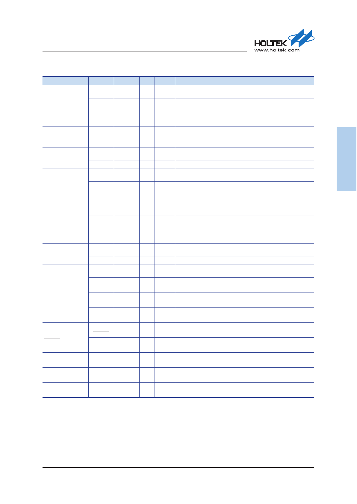
3
Selection Table
Most features are common to all devices, the main feature distinguishing them are Program
Memory and Data memory capacity, A/D channels, UART numbers and packages. The following
table summarises the main features of each device.
Part No. V
HT85F2260 2.2V~5.5V 16K×8 1280×8 32 7 4 CCU×4 1
HT85F2270 2.2V~5.5V 32K×8 2304×8 48 7 4 CCU×4 1
HT85F2280 2.2V~5.5V 64K×8 2304×8 48 7 4 CCU×4 1
Part No. A/D D/A Comparator I2C SPI UART
HT85F2260 12-bit×7 12-bit×1 2 √ √ 1 √ 48LQFP
HT85F2270 12-bit×9 12-bit×1 2 √ √ 2 √ 48/64LQFP
HT85F2280 12-bit×9 12-bit×1 2 √ √ 2 √ 48/64LQFP
Note:
CCU stands for Compare/Capture Unit.
DD
Program
Memory
Data
Memory
I/O
Ext.
Interrupt
16-bit Timer 16-bit PCA Time Base
Temp.
Sensor
package
Selection Table
Rev. 1.00 17 of 225 January 15, 2015
Page 18
Standard 8051 8-Bit Flash MCU
HT85F2260/HT85F2270/HT85F2280
4
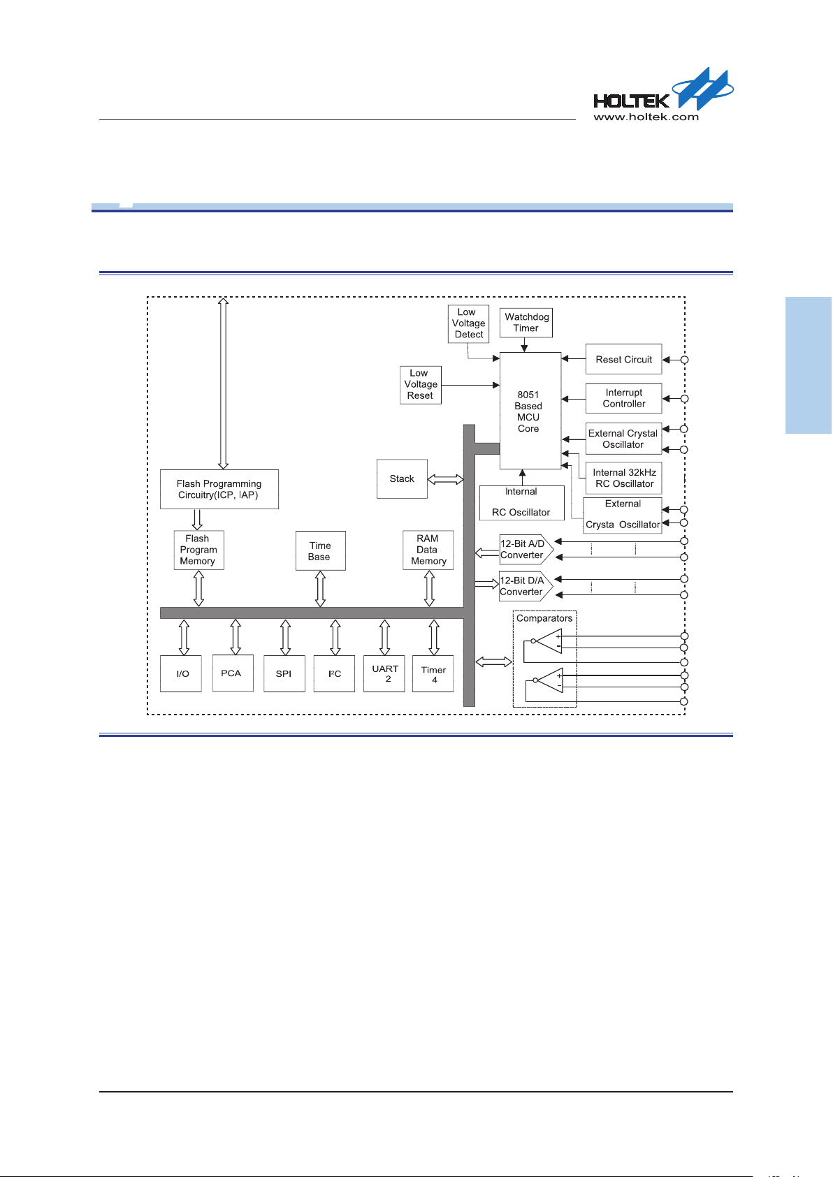
Block Diagram
The following block diagram illustrates the main functional blocks.
3.6864MHz
32768Hz
I
Block Diagram
× ×
Rev. 1.00 18 of 225 January 15, 2015
Page 19
Standard 8051 8-Bit Flash MCU
HT85F2260/HT85F2270/HT85F2280
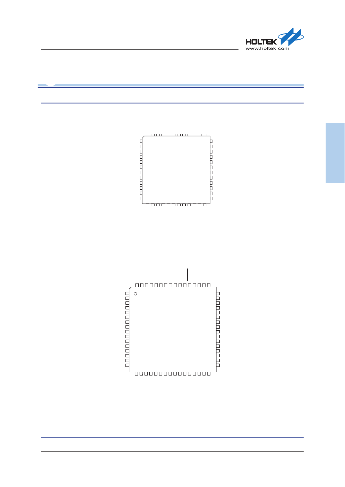
5
Pin Assignment
Pin Assignment
Note:
1. If the pin-shared pin functions have multiple outputs simultaneously, its pin names at the right side of the “/”
sign can be used for higher priority.
2. For both the 48 LQFP-A and 64 LQFP-A packages, both real IC and OCDS EV IC share the same
package.
Rev. 1.00 19 of 225 January 15, 2015
Page 20
Standard 8051 8-Bit Flash MCU
HT85F2260/HT85F2270/HT85F2280
6
Pin Descriptions
With the exception of the power pins, all pins on these devices can be referenced by their Port
name, e.g. P0.0, P0.1 etc, which refer to the digital I/O function of the pins. However these Port
pins are also shared with other function such as the Analog to Digital Converter, Serial Port pins
etc. The function of each pin is listed in the following table, however the details behind how each
pin is congured is contained in other sections of the datasheet.
Pin Name Function OPT I/T O/T Description
P0.0/ICPDA/TDA
P0.1/C1OUT
P0.2/SSN
P0.3/SCK
P0.4/MISO
P0.5/MOSI
P0.6/SCL
P0.7/SDA
P1.0/INT3/CC0
P1.1/INT4/CC1
P1.2/INT5/CC2
P0.0
ICPDA — ICP Data Input/Output
TDA — Debug Data Input/Output
P0.1
C1OUT — — CMOS Comparator 1 Output
P0.2
SSN — ST — SPI Slave select Input
P0.3
SCK — ST CMOS SPI Clock
P0.4
MISO — ST CMOS SPI Master In Slave Out pin
P0.5
MOSI — ST CMOS SPI Master Out Slave In pin
P0.6
SCL — — NMOS I2C Clock
P0.7
SDA — — NMOS I2C Data
P1.0
INT3 — ST — External Interrupt 3 Input
CC0 — ST CMOS Compare/Capture input/output for PCA module 0
P1.1
INT4 — ST — External Interrupt 4 Input
CC1 — ST CMOS Compare/Capture input/output for PCA module 1
P1.2
INT5 — ST — External Interrupt 5 Input
CC2 — ST CMOS Compare/Capture input/output for PCA module 2
P0M0
P0M1
P0WAKE
P0M0
P0M1
P0WAKE
P0M0
P0M1
P0WAKE
P0M0
P0M1
P0WAKE
P0M0
P0M1
P0WAKE
P0M0
P0M1
P0WAKE
P0M0
P0M1
P0WAKE
P0M0
P0M1
P0WAKE
P1M0
P1M1
P1M0
P1M1
P1M0
P1M1
ST CMOS
ST CMOS
ST CMOS General purpose I/O. Register selected I/O mode and wake-up
ST CMOS
ST CMOS
ST CMOS General purpose I/O. Register selected I/O mode and wake-up
ST CMOS
ST CMOS
ST CMOS
ST CMOS
ST CMOS General purpose I/O. Register selected I/O mode
General purpose I/O. Register selected I/O mode and wake-up
General purpose I/O. Register selected I/O mode and wake-up
General purpose I/O. Register selected I/O mode and wake-up
General purpose I/O. Register selected I/O mode and wake-up
General purpose I/O. Register selected I/O mode and wake-up
General purpose I/O. Register selected I/O mode and wake-up
General purpose I/O. Register selected I/O mode
General purpose I/O. Register selected I/O mode
Pin Descriptions
Rev. 1.00 20 of 225 January 15, 2015
Page 21

Standard 8051 8-Bit Flash MCU
HT85F2260/HT85F2270/HT85F2280
Pin Name Function OPT I/T O/T Description
P1.3
P1.3/INT6/CC3
P1.4/INT2
P1.5/T2EX
P1.6/T2
P1.7 P1.7
P2.0~P2.6 P2.0~P2.6
P2.7/T3
P3.0/RXD0
P3.1/TXD0
P3.2/INT0
P3.3/INT1
P3.4/T0
P3.5/T1
P3.6/RXD1
P3.7/TXD1
P4.0/AIN.0
P4.1/AIN.1
P4.2/AIN.2
INT6 — ST — External Interrupt 6 Input
CC3 — ST CMOS Compare/Capture input/output for PCA module 3
P1.4
INT2 — ST — External Interrupt 2 Input
P1.5
T2EX — ST — Timer 2 capture trigger
P1.6
T2 — ST CMOS Timer 2 external input or Timer 2 programmable clock output
P2.7
T3 — ST — Timer 3 External Input
P3.0
RXD0 — ST — UART0 Receive Data Input
P3.1
TXD0 — — CMOS UART0 Transmit Data Output
P3.2
INT0 — ST — External Interrupt 0 Input
P3.3
INT1 — ST — External Interrupt 1 Input
P3.4
T0 — ST — Timer 0 External Input
P3.5
T1 — ST — Timer 1 External Input
P3.6
RXD1 — ST — UART1 Receive Data Input
P3.7
TXD1 — — CMOS UART1 Transmit Data Output
P4.0
AIN.0 — AN — ADC Input Channel 0
P4.1
AIN.1 — AN — ADC Input Channel 1
P4.2
AIN.2 — AN — ADC Input Channel 2
P1M0
P1M1
P1M0
P1M1
P1M0
P1M1
P1M0
P1M1
P1M0
P1M1
P2M0
P2M1
P2M0
P2M1
P3M0
P3M1
P3M0
P3M1
P3M0
P3M1
P3M0
P3M1
P3M0
P3M1
P3M0
P3M1
P3M0
P3M1
P3M0
P3M1
P4M0
P4M1
P4M0
P4M1
P4M0
P4M1
ST CMOS
ST CMOS General purpose I/O. Register selected I/O mode
ST CMOS
ST CMOS General purpose I/O. Register selected I/O mode
ST CMOS General purpose I/O. Register selected I/O mode
ST CMOS General purpose I/O. Register selected I/O mode
ST CMOS General purpose I/O. Register selected I/O mode
ST CMOS
ST CMOS
ST CMOS General purpose I/O. Register selected I/O mode
ST CMOS
ST CMOS
ST CMOS General purpose I/O. Register selected I/O mode
ST CMOS
ST CMOS
ST CMOS
ST CMOS
ST CMOS General purpose I/O. Register selected I/O mode
General purpose I/O. Register selected I/O mode
General purpose I/O. Register selected I/O mode
General purpose I/O. Register selected I/O mode
General purpose I/O. Register selected I/O mode
General purpose I/O. Register selected I/O mode
General purpose I/O. Register selected I/O mode
General purpose I/O. Register selected I/O mode
General purpose I/O. Register selected I/O mode
General purpose I/O. Register selected I/O mode
General purpose I/O. Register selected I/O mode
Pin Descriptions
Rev. 1.00 21 of 225 January 15, 2015
Page 22
Standard 8051 8-Bit Flash MCU
HT85F2260/HT85F2270/HT85F2280
Pin Name Function OPT I/T O/T Description
P4.3/AIN.3
P4.4/AIN.4
P4.5/AIN.5
P4.6/AIN.6
P4.7/AIN.7
P5.0~P5.3 P5.0~P5.3
P5.4/C0OUT
P5.5/XT1
P5.6/XT2
P5.7/DAC
CP0-/CP0+
CP1-/CP1+
OSC1 OSC1 — HXT — High Frequency Crystal Oscillator
OSC2 OSC2 — — HXT High Frequency Crystal Oscillator
RESET/ICPCK/TCK
VREF VREF — AN — Reference Voltage for ADC/DAC
VDD VDD — PWR — Positive Power supply for CORE
VCCA1 VCCA1 — PWR — Positive Power supply for I/O pad
VCCA2 VCCA2 — PWR — Positive Power supply for DAC
VCCA3 VCCA3 — PWR — Positive Power supply for ADC
VSS VSS — PWR — Negative Power supply
P4.3
AIN.3 — AN — ADC Input Channel 3
P4.4
AIN.4 — AN — ADC Input Channel 4
P4.5
AIN.5 — AN — ADC Input Channel 5
P4.6
AIN.6 — AN — ADC Input Channel 6
P4.7
AIN.7 — AN — ADC Input Channel 7
P5.4
C0OUT — — CMOS Comparator 0 Output
P5.5
XT1 — LXT — Low Frequency Crystal Oscillator
P5.6
XT2 — — LXT Low Frequency Crystal Oscillator
P5.7
DAC — — CMOS DAC Output
CP0- — AN —
CP0+ — AN — Comparator 0 Non-Inverting Input
CP1- — AN —
CP1+ — AN — Comparator 1 Non-Inverting Input
RESET — ST — RESET pin
ICPCK — ST —
TCK — ST — Debug Clock Input
P4M0
P4M1
P4M0
P4M1
P4M0
P4M1
P4M0
P4M1
P4M0
P4M1
P5M0
P5M1
P5M0
P5M1
P5M0
P5M1
P5M0
P5M1
P5M0
P5M1
ST CMOS
ST CMOS
ST CMOS General purpose I/O. Register selected I/O mode
ST CMOS
ST CMOS
ST CMOS General purpose I/O. Register selected I/O mode
ST CMOS General purpose I/O. Register selected I/O mode
ST CMOS General purpose I/O. Register selected I/O mode
ST CMOS General purpose I/O. Register selected I/O mode
ST CMOS General purpose I/O. Register selected I/O mode
General purpose I/O. Register selected I/O mode
General purpose I/O. Register selected I/O mode
General purpose I/O. Register selected I/O mode
General purpose I/O. Register selected I/O mode
Comparator 0 Inverting Input
Comparator 1 Inverting Input
ICP Clock Input
Pin Descriptions
Note:
I/T: Input type; O/T: Output type; ST: Schmitt Trigger input
OPT: Optional by conguration option (CO) or register option
PWR: Power; NMOS: NMOS output
CMOS: CMOS output; AN: Analog input pin
LXT: low frequency crystal oscillator; HXT: high frequency crystal oscillator
Where devices exist in more than one package type the table reflects the situation for the package with the
largest number of pins. For this reason not all pins described in the table may exist on all package types.
Rev. 1.00 22 of 225 January 15, 2015
Page 23
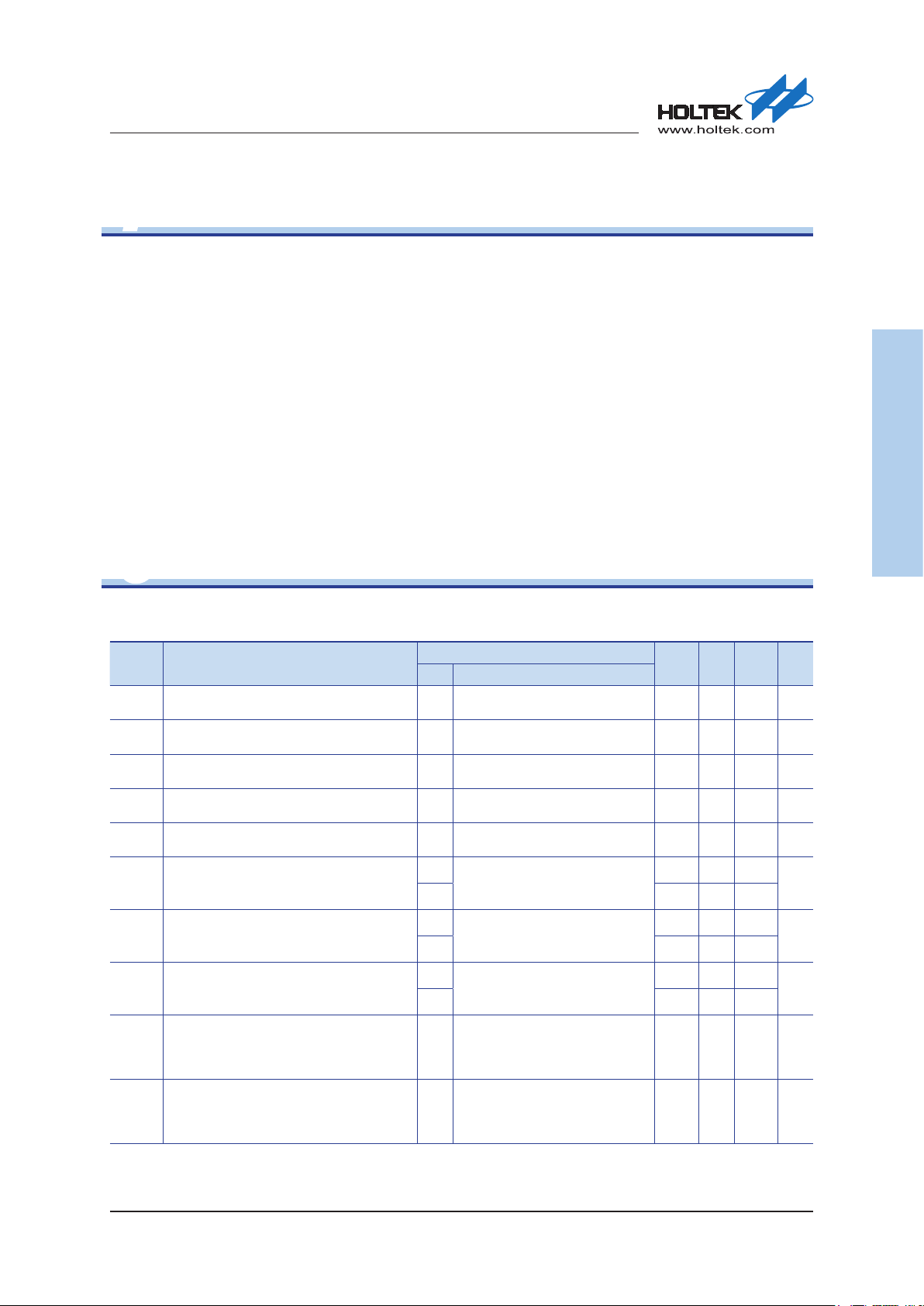
Standard 8051 8-Bit Flash MCU
HT85F2260/HT85F2270/HT85F2280
7
Absolute Maximum Ratings
Supply Voltage .................................................................................................VSS-0.3V to VDD+6.0V
Input Voltage ................................................................................................... VSS-0.3V to VDD+0.3V
Storage Temperature ...................................................................................................-50°C to 125°C
Operating Temperature ................................................................................................ -40°C to 85°C
Tot al
I
......................................................................................................................................150mA
OL
IOH Tota l ................................................................................................................................... -100m A
Total Power Dissipation ...........................................................................................................5 00mW
Note: These are stress ratings only. Stresses exceeding the range specified under “Absolute
Maximum Ratings” may cause substantial damage to the device. Functional operation of
this device at other conditions beyond those listed in the specification is not implied and
prolonged exposure to extreme conditions may affect device reliability.
8
Symbol Parameter
V
DD1
V
DD2
V
DD3
V
DD4
V
DD5
I
DD1
I
DD2
I
DD3
I
DD4
I
DD5
D.C. Characteristics
Operating Voltage
(High Frequency Internal RC OSC)
Operating Voltage
(Crystal OSC)
Operating Voltage
(PLL)
Operating Voltage
(PLL)
Operating Voltage
(PLL)
Operating Current
(High Frequency Internal RC OSC)
Operating Current
(Crystal OSC)
Operating Current (PLL)
Operating Current (PLL) 5V
Operating Current (PLL) 5V
Test Conditions
V
DD
f
OSC=fSYS
—
(PLL disabled)
f
OSC=fSYS
—
(PLL disabled)
f
OSC
—
f
=12MHz (PLL × 3)
SYS
f
OSC
—
f
=16MHz (PLL × 4)
SYS
f
OSC
—
f
=24MHz (PLL × 6)
SYS
No load, f
3V
(PLL disabled) ADC off, DAC off,
5V — 10.0 15.0
WDT enable
No load, f
3V
(PLL disabled)
5V — 12.5 20
ADC off, DAC off, WDT enable
No load, f
3V
f
=12MHz (PLL × 3)
SYS
5V — 16 25
ADC off, DAC off, WDT enable
No load,
f
OSC
f
=16MHz (PLL × 4)
SYS
ADC off, DAC off, WDT enable
No load,
f
OSC
f
=24MHz (PLL × 6)
SYS
ADC off, DAC off, WDT enable
Conditions
=3.6864MHz
=8MHz
=4MHz (Crystal OSC)
=4MHz (Crystal OSC)
=4MHz (Crystal OSC)
=3.6864MHz ,
OSC=fSYS
=8MHz ,
OSC=fSYS
=4MHz (Crystal OSC)
OSC
=4MHz (Crystal OSC)
=4MHz (Crystal OSC)
Min. Typ. Max. Unit
2.2 — 5.5 V
2.2 — 5.5 V
2.7 — 5.5 V
3.3 — 5.5 V
4.5 — 5.5 V
— 5.0 8.0
— 6.0
— 8.0
— 20 30 mA
— 28 40 mA
8.5
12.0
Absolute Maximum Ratings
Ta=25°C
mA
mA
mA
Rev. 1.00 23 of 225 January 15, 2015
Page 24

Standard 8051 8-Bit Flash MCU
HT85F2260/HT85F2270/HT85F2280
Symbol Parameter
I
I
V
V
V
V
I
I
I
I
STB1
STB2
OL
OH1
OH2
IL
Stanby Current
r-Down mode)(HIRC off, HXT off)
(Powe
Stanby Current (Idle)
(HIRC off, HXT on)
Input Low Voltage (except RESET pin) — quasi-bidirection mode 0 — 0.2VDDV
IL1
Input High Voltage (except RESET pin) — quasi-bidirection mode 0.8VDD— V
IH1
Input Low Voltage (RESET pin) — — 0 — 0.4VDDV
IL2
Input High Voltage (RESET pin) — — 0.9VDD— V
IH2
I/O Port Sink Current
I/O Port Source Current
(push-pull mode for Ports 0, 1, 2, 3)
I/O Port Source Current
(quasi-bidirection mode for Ports 0, 1, 2, 3, 4, 5)
Logical 0 input current, Ports 0, 1, 2, 3, 4, 5
(quasi-bidirection mode)
Logical 1 to 0 transition
I
TL
Current, Ports 0, 1, 2, 3, 4, 5
(quasi-bidirection mode)
I
LI
V
I
BG
I
LVR
I
LVD
V
V
V
V
V
V
V
V
V
V
V
V
Input Leakage current, Ports 0, 1, 2, 3
(input mode)
Bandgap reference with buffer voltage
BG
(for A/D type MCU Tiny Power IP)
Additional Power Consumption if Reference
with Buffer is used (for A/D type MCU)
Additional Power Consumption if LVR is used
(for Tiny Power IP)
Additional Power Consumption if LVD is used
(for Tiny Power IP)
LVR1
LVR2
Low Voltage Reset Voltage —
LVR3
LVR4
LVD1
LVD2
LVD3
LVD4
Low Voltage Detector Voltage —
LVD5
LVD6
LVD7
LVD8
Test Conditions
V
DD
3V
No load, All peripherals off
5V — — 2.5
No load, f
3V
f
off, ADC off, DAC off,
SYS
5V — 3.5 5.0
LVD/LVR disable, WDT enable,
Conditions
=4MHz (Crystal OSC)
OSC
2.2V
Min. Typ. Max. Unit
— —
1.5
— 1.5 2.5
DD
DD
— 6.0 —
VOL=0.4V
5.0V — 12.0 —
2.2V
VOH=0.9V
DD
— -1.0 —
-2.0 —
5.0V — -4.0 —
2.2V
VOH=0.9V
DD
— -40 —
5.0V — -160 —
5V VIN=0.4V — — -50 μA
5V VIN=2.4V — — -950 μA
5V 0.45V<VIN<VDD-0.3 — — ±10 μA
— — -3% 1.1 +3% V
— — — 200 300 μA
3V
LVR enable
5V — 75 100
3V
LVD enable
5V — 75 100
LVR Enable
, 2.1V select
LVR Enable, 2.55V select 2.55
LVR Enable, 3.15V select 3.15
—
—
-5%
75 100
75 100
2.1
+5% V
LVR Enable, 4.0V select 4.0
LVD Enable
, 2.0V Select
2.0
LVD Enable, 2.2V Select 2.2
LVD Enable, 2.4V Select 2.4
LVD Enable, 2.7V Select 2.7
LVD Enable, 3.0V Select 3.0
-5%.
+5% V
LVD Enable, 3.3V Select 3.3
LVD Enable, 3.6V Select 3.6
LVD Enable, 4.2V Select 4.2
μA
mA
D.C. Characteristics
V
V
mA3.3V — 9.0 —
mA3.3V —
μA3.3V — -80 —
μA
μA
Rev. 1.00 24 of 225 January 15, 2015
Page 25

Standard 8051 8-Bit Flash MCU
HT85F2260/HT85F2270/HT85F2280
9
A.C. Characteristics
Symbol Parameter
f
SYS1
f
SYS2
f
LIRC
f
HIRC
f
TIMER
t
RES
System clock (Crystal OSC)
System clock (PLL) 4.5V~5.5V Crystal OSC=4MHz, PLL Enable 4 — 32 MHz
32kHz Internal RC oscillator
3.6864MHz Internal RC oscillator
Timer Input Frequency (T0~T3)
External Reset Minimum Low Pulse width — — 1 3.3 5 μs
System start-up timer period (Power-up or
t
SST
wake-up from Power-Down mode when
the main oscillator is off or system clock is
switching between HXT and HIRC)
t
RSTD
t
SRESET
t
HTO
t
INT
t
LVR
System Reset Delay Time (LVR reset) — — 16 32 64 ms
Software Reset Width to Reset — — 45 90 120 μs
HIRC Turn On Period 2.2V~5.5V HIRC OFF → ON — 200 — μs
External Interrupt Minimum Pulse Width —
Low Voltage Width to Reset — — 120 240 480 μs
Ta=25°C
Test Conditions
V
DD
Conditions
2.2V~5.5V
PLL Disable
4.5V~5.5V 0.4 — 24
5V Ta=25°C -10% 32 +10%
2.2V~5.5V Ta=-40°C~85°C -50% 32 +60%
Ta=25°C -3% 3.6864 +3%
3V
5V Ta=25°C -3% 3.6864 +3%
2.2V~5.5V f
4.5V~5.5V f
— f
=8MHz 0 — 2
SYS
=12MHz 0 — 3
SYS
=24MHz 0 — 6
SYS
=HXT or HIRC — 1024 — t
SYS
MCU is in Normal mode or Idle
mode
Min. Typ. Max. Unit
0.4 — 8
— 4 — t
MHz2.7V~5.5V 0.4 — 12
kHz
MHz
MHz2.7V~5.5V f
SYS
SYS
A.C. Characteristics
Rev. 1.00 25 of 225 January 15, 2015
Page 26
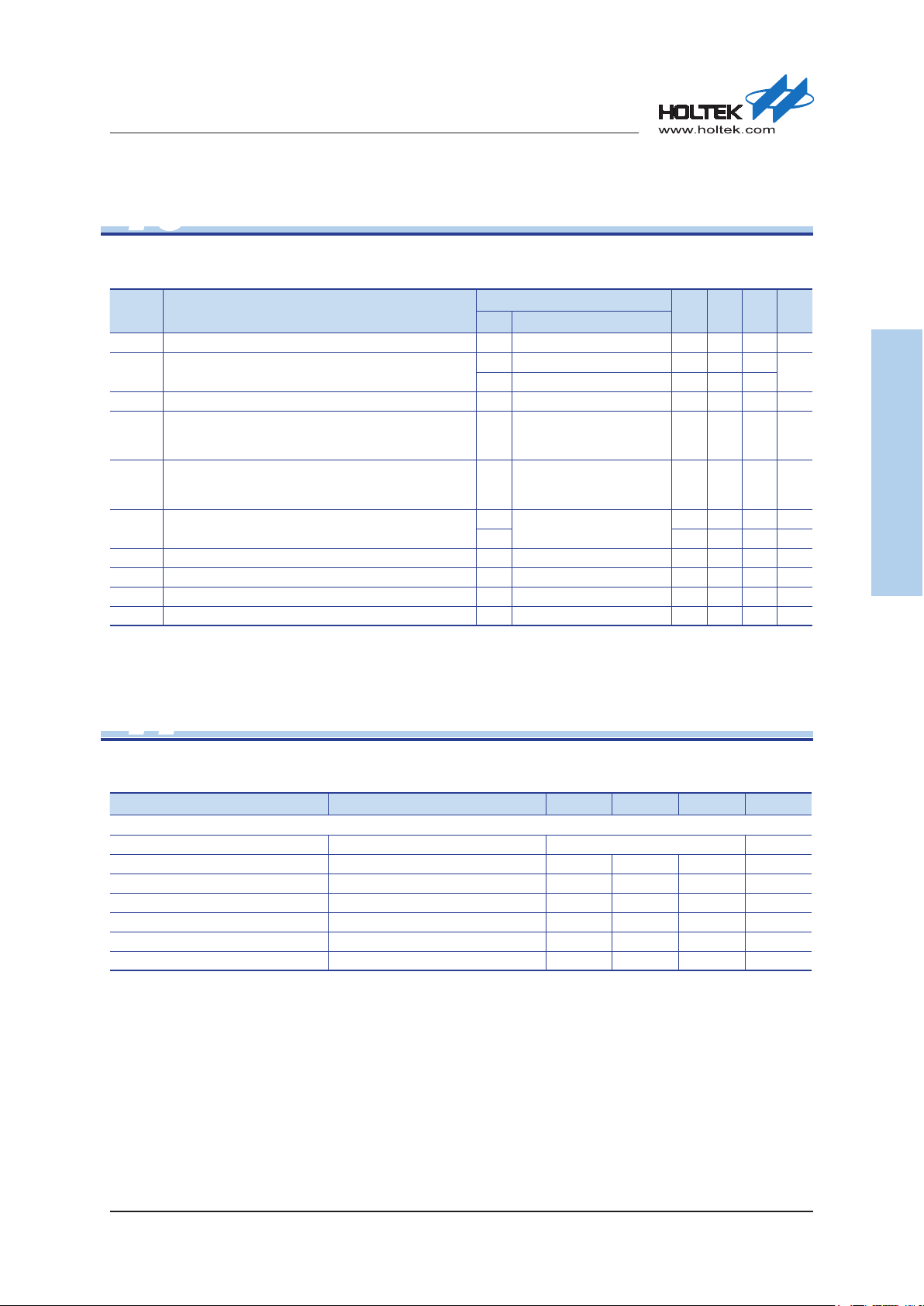
Standard 8051 8-Bit Flash MCU
HT85F2260/HT85F2270/HT85F2280
10
Symbol Parameter
AV
V
V
DNL
INL
I
ADC
t
ADCK
t
ADC
t
ADS
t
ON2ST
A/D Converter Operating Voltage — — 2.7 — 5.5 V
DD
A/D Converter Input Voltage
ADI
A/D Converter Reference Voltage — — 2 — AVDDV
REF
Differential Non-linearity —
Integral Non-linearity —
Additional Power Consumption if A/D Converter is used
A/D Converter Clock Period — — 0.5 — 10 μs
A/D Conversion Time (Include Sample and Hold Time) — 12 bit ADC — 16 — t
A/D Converter Sampling Time — — — 4 — t
ADC on to ADC start — — 2 — — μs
ADC Electrical Characteristics
Ta=25°C
Test Conditions
AV
=5V
DD
V
=AV
REF
t
=1μs
ADCK
AVDD=5V
V
REF=AVDD
t
=1μs
ADCK
No load, t
Conditions
DD
=0.5μs
ADCK
V
DD
— VREF available 0 — V
— VREF not available 0 — AV
3V
5V — 1.30 2.00 mA
Min. Typ. Max. Unit
REF
DD
-2 — +2 LSB
-4 — +4 LSB
— 1.00 1.40 mA
ADCK
ADCK
ADC Electrical Characteristics
V
11
Static Performance
Resolution — 12 bits
Integral Nonlinearity — — ±2 — LSB
Differential Nonlinearity — — — ±1 LSB
Offset Error Data Word=0x014 — ±3 ±30 mV
Gain Error — — ±20 ±60 mV
Output Sink Current — — 300 — μA
Output Short-Circuit Current Data Word=0xFFF — 15 — mA
DAC Electrical Characteristics
VDD=3V, AV+=3.0V, V
Parameter Test Conditions Min. Typ. Max. Units
=2.4V, no output load unless otherwise specied
REF
Rev. 1.00 26 of 225 January 15, 2015
Page 27
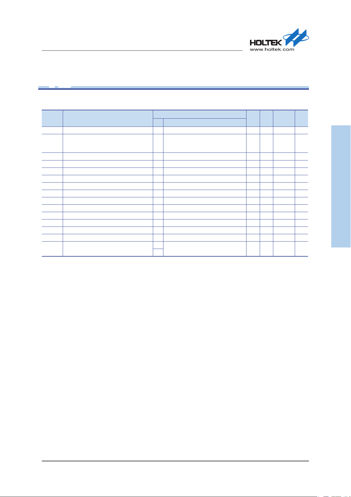
Standard 8051 8-Bit Flash MCU
HT85F2260/HT85F2270/HT85F2280
12
Symbol
—
—
—
V
CMPOS
V
HP1
V
HP2
V
HP3
V
HP4
V
HN1
V
HN2
V
HN3
V
HN4
V
CM
A
OL
t
PD
Note:
Comparator operating voltage — — 2.2 — 5.5 V
Comparator operating current 5V
Comparator power-down current 5V Comparator disable — — 0.1 μA
Comparator input offset voltage 5V — -10 — +10 mV
Positive Hysteresis 1 5V CP(n)HP[1:0]=00b — 0 1 mV
Positive Hysteresis 2 5V CP(n)HP[1:0]=01b 3 6 10 mV
Positive Hysteresis 3 5V CP(n)HP[1:0]=10b 6 13 20 mV
Positive Hysteresis 4 5V CP(n)HP[1:0]=11b 12 25 40 mV
Negative Hysteresis 1 5V CP(n)HN[1:0]=00b — 0 1 mV
Negative Hysteresis 2 5V CP(n)HN[1:0]=01b 3 6 10 mV
Negative Hysteresis 3 5V CP(n)HN[1:0]=10b 6 13 20 mV
Negative Hysteresis 4 5V CP(n)HN[1:0]=11b 12 25 40 mV
Comparator common mode voltage range — — VSS— VDD-1.4V V
Comparator open loop gain — — 60 80 — dB
Comparator response time
Measured with comparator one input pin at VCM=(VDD-1.4)/2 while the other pin input transition from VSS to
Comparator Electrical Characteristics
Parameter
Test Conditions
V
DD
LVDCR=00h, ADCR1=08h, i.e. select
internal bandgap voltage output (x2)
as VREFI
3V
With 100mV overdrive — 4 — μs
5V
Conditions
Min. Typ. Max.
— — 10 μA
(VCM +100mV) or from VDD to (VCM -100mV).
Ta=25°C
Unit
Comparator Electrical Characteristics
Rev. 1.00 27 of 225 January 15, 2015
Page 28
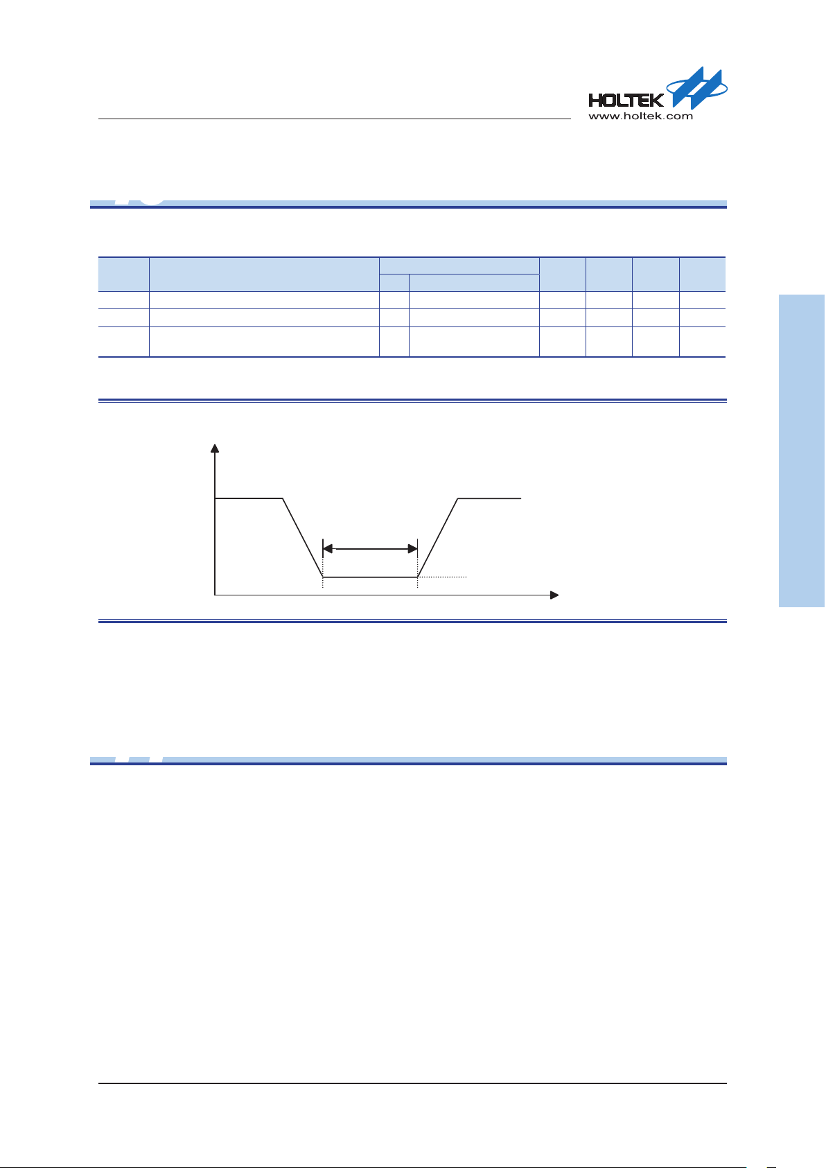
Standard 8051 8-Bit Flash MCU
HT85F2260/HT85F2270/HT85F2280
13
Symbol Parameter
V
RR
t
POR
POR
VDD Start Voltage to ensure Power-on Reset — — — — 100 mV
VDD Rising Rate to ensure Power-on Reset — — 0.035 — — V/ms
POR
Minimum Time for VDD stays at V
Power-on Reset
Power on Reset Electrical Characteristics
to ensure
POR
Test Conditions
V
DD
— — 1 — — ms
Conditions
Min. Typ. Max. Unit
Ta=25°C
Power on Reset Electrical Characteristics
14
Rev. 1.00 28 of 225 January 15, 2015
System Architecture
A key factor in the high-performance features of the Holtek range of microcontrollers is attributed
to their internal system architecture. The range of devices take advantage of the usual features
found within 8051-based microcontrollers providing increased speed of operation and enhanced
performance. The pipelining scheme is implemented in such a way that instruction fetching and
instruction execution are overlapped, hence most instructions are effectively executed in one clock
cycle, with the exception of branch or call instructions. Compared with classic MCU architecture,
the 8051-based core runs at a much higher speed and with greatly reduced power consumption. An
8-bit wide ALU is used in practically all operations of the 8051 compatible instruction set. It carries
out arithmetic operations, logic operations, rotation, increment, decrement, branch decisions, etc.
The internal data path is simplied by moving data through the Accumulator and the ALU. Certain
internal registers are implemented in the Data Memory and can be directly or indirectly addressed.
The simple addressing methods of these registers along with additional architectural features
ensure that a minimum of external components is required to provide a functional I/O control
system with maximum reliability and exibility.
Page 29
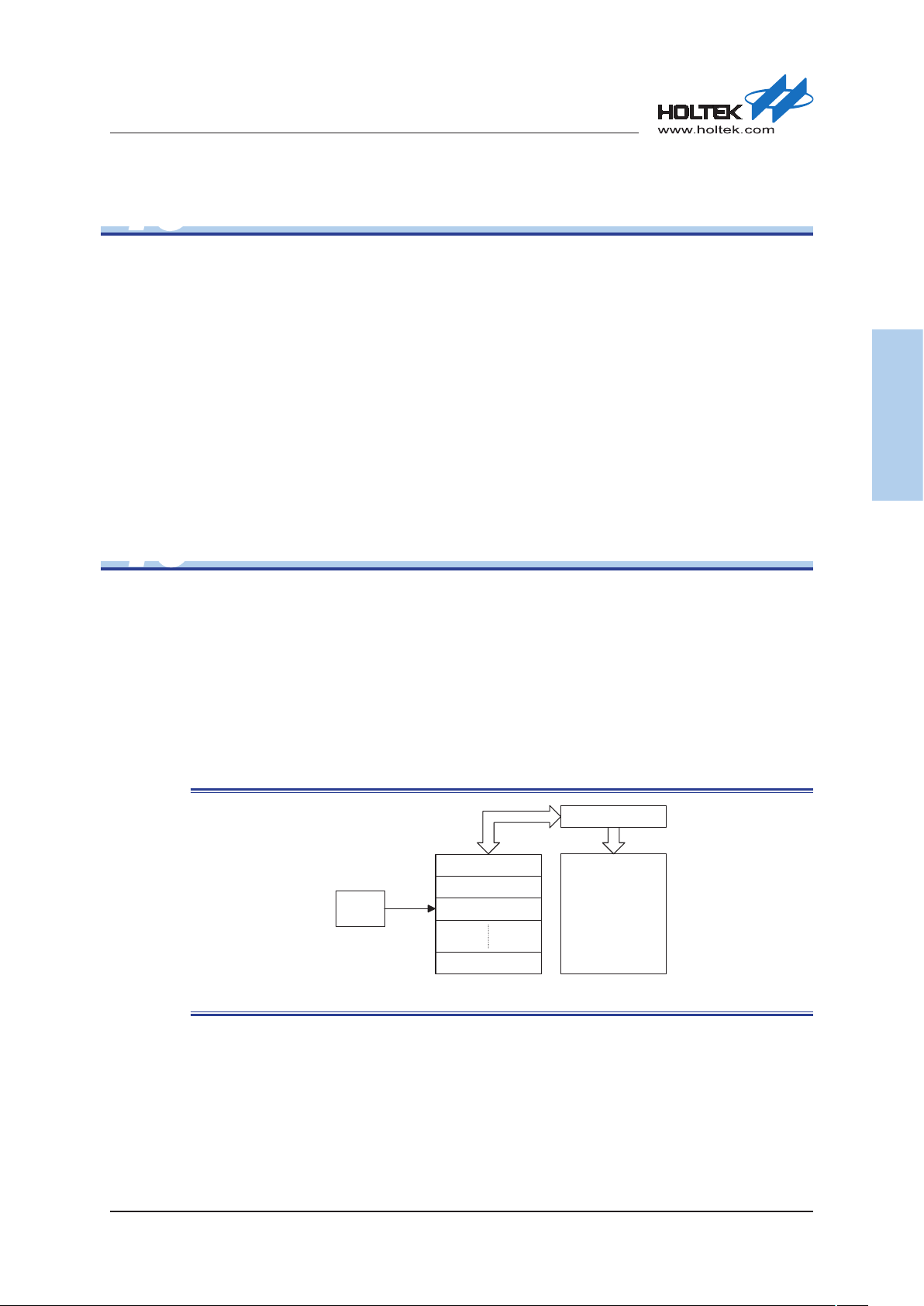
Standard 8051 8-Bit Flash MCU
HT85F2260/HT85F2270/HT85F2280
15
During program execution, the Program Counter is used to keep track of the address of the
next instruction to be executed. It is automatically incremented by one each time an instruction
is executed except for instructions, such as “JMP” or “CALL” that demand a jump to a
non-consecutive Program Memory address.
When executing instructions requiring jumps to non-consecutive addresses such as a jump
instruction, a subroutine call, interrupt or reset, etc., the microcontroller manages program control
by loading the required address into the Program Counter. For conditional skip instructions, once
the condition has been met, the next instruction, which has already been fetched during the present
instruction execution, is discarded and a dummy cycle takes its place while the correct instruction
is obtained.
16
This is a special part of the memory which is used to save the contents of the Program Counter
only. The stack is located in the 256 byte Data memory; therefore, the depth can be extended
up to 256 levels. The activated level is indexed by the Stack Pointer, SP, and is neither readable
nor writeable. At a subroutine call or interrupt acknowledge signal, the contents of the Program
Counter are pushed onto the stack. At the end of a subroutine or an interrupt routine, signaled by
a return instruction, RET or RETI, the Program Counter is restored to its previous value from the
stack. After a device reset, the Stack Pointer will point to the location 0x07, the top of the stack.
Note that if the data memory has been used as the stack area, it should not be used as general
purpose Data RAM.
Program Counter
Program Counter
Stack
Progra m Counte r
T op of S ta ck
Stack
Poin te r
Bottom o f Stack
Stack Block Diagram
If the stack is full and an enabled interrupt takes place, the interrupt request ag will be recorded
but the acknowledge signal will be inhibited. When the Stack Pointer is decremented, by RET or
RETI, the interrupt will be serviced. This feature prevents stack overow allowing the programmer
to use the structure more easily. However, when the stack is full, a CALL subroutine instruction
can still be executed which will result in a stack overow. Precautions should be taken to avoid
such cases which might cause unpredictable program branching.
Rev. 1.00 29 of 225 January 15, 2015
Stack Level 1
Stack Level 2
Stack Level 3
Stack Level 256
Progra m
Memory
Page 30

Standard 8051 8-Bit Flash MCU
HT85F2260/HT85F2270/HT85F2280
17
The arithmetic-logic unit or ALU is a critical area of the microcontroller that carries out arithmetic
and logic operations of the instruction set. Connected to the main microcontroller data bus,
the ALU receives related instruction codes and performs the required arithmetic or logical
operations after which the result will be placed in the specied register. As these ALU calculation
or operations may result in carry, borrow or other status changes, the status register will be
correspondingly updated to reect these changes. The ALU supports the following functions:
■
■
■
■
■
Arithmetic and Logic Unit – ALU
Arithmetic and Logic Unit – ALU
Arithmetic operations: ADD, ADDC, SUBB, DA, MUL, DIV
Logic operations: ANL, ORL, XRL, CLR, CPL
Rotation: RL, RLC, RR, RRC, SWAP
Increment and Decrement: INC, DEC
Branch decision: JC, JNC, JB, JNB, JBC, ACALL, LCALL, RET, RETI, AJMP, SJMP, JMP, JZ,
JNZ, CJNE, DJNZ
Rev. 1.00 30 of 225 January 15, 2015
Page 31

Standard 8051 8-Bit Flash MCU
3FFFH
Reset
0000H
HT85F2260
0003H
00ABH
HT85F2270 HT85F2280
Interrupt
Vector
8 bits
8 bits
8 bits
Reset
Interrupt
Vector
Reset
Interrupt
Vector
7FFFH
FFFFH
HT85F2260/HT85F2270/HT85F2280
18
Flash Program Memory
The Program Memory is the location where the user code or program is stored. For these devices
the Program Memory is Flash type, which means it can be programmed and re-programmed
a large number of times, allowing the user the convenience of code modification on the same
device. By using the appropriate programming tools, these Flash devices offer users the exibility
to conveniently debug and develop their applications while also offering a means of field
programming and updating.
Structure
The Program Memory has a capacity from 16K×8 to 64K×8. The Program Memory is addressed
by the Program Counter and also contains data, table information and interrupt entries. Table data,
which can be setup in any location within the Program Memory, is addressed by a separate table
pointer register.
Special Vectors
Within the Program Memory, certain locations are reserved for the reset and interrupts. The
location 000H is reserved for use by the device reset for program initialisation. After a device reset
is initiated, the program will jump to this location and begin execution.
Flash Program Memory
Program Memory Structure
Rev. 1.00 31 of 225 January 15, 2015
Page 32

Standard 8051 8-Bit Flash MCU
HT85F2260/HT85F2270/HT85F2280
In-Circuit Programming – ICP
The provision of Flash type Program Memory provides the user with a means of convenient
and easy upgrades and modifications to their programs on the same device. As an additional
convenience, Holtek has provided a means of programming the microcontroller in-circuit using
a four-line serial interface. This provides manufacturers with the possibility of manufacturing
their circuit boards complete with a programmed or un-programmed microcontroller, and then
programming or upgrading the program at a later stage. This enables product manufacturers to
easily keep their manufactured products supplied with the latest program releases without removal
and re-insertion of the device.
The Holtek Flash MCU to Writer Programming Pin correspondence table is as follows:
Holtek Writer Pins MCU Programming Pins Function
ICPDA P0.0/ICPDA
ICPCK RESET/ICPCK Programming Serial Clock
VDD VDD Power Supply
VSS VSS Ground
Flash Program Memory
Programming Serial Data/Address
The Program Memory can be programmed serially in-circuit using the interface on pins ICPDA
and ICPCK. Data is downloaded and uploaded serially on a single pin with an additional line for the
clock. Two additional lines are required for the power supply. The technical details regarding the
in-circuit programming of the device are beyond the scope of this document and will be supplied in
supplementary literature. The Flash Program Memory Read/Write function is implemented using a
series of registers.
On-Chip Debug Support – OCDS
An EV chip, HT85V2280, is provided which includes all the HT85F2280 functions as well as an
“On-Chip Debug” interface for emulation of the HT85F2280/2270/2260 devices. To minimise
the difference between the real IC (the volume-production version) and the EV chip (the device
with the debug interface), a protocol converter is implemented to translate the external 2-wire
connections (TCK and TDA) into 4 internal JTAG signals (TCK, TMS, TDI, and TDO) and vice
versa. Users can use the EV chip device to emulate the real chip device behavior by connecting
the TDA and TCK pins to the related Holtek development tools. The TDA pin is the OCDS
Data/Address input/output pin while the TCK pin is the OCDS clock input pin. When users use the
EV chip for debugging, other functions which are shared with the TDA and TCK pins in the actual
MCU device will have no effect in the EV chip. However, the two OCDS pins which are pin-shared
with the ICP programming pins are still used as the Flash Memory programming pins for ICP. For
a more detailed OCDS description, refer to the corresponding user’s guide.
Rev. 1.00 32 of 225 January 15, 2015
Page 33

Standard 8051 8-Bit Flash MCU
HT85F2260/HT85F2270/HT85F2280
In-Application Programming – IAP
An In-Application Programming interface is provided to allow the end user’s application to erase
and reprogram the user code memory. No extra code memory block (bootloader) is required to
update the rmware or non-volatile data. Firmware for the IAP and the code memory to be updated
are physically on the same IP. Users could update rmware or non-volatile data except for the sector
where IAP is located and run. A rmware library is used to provide APIs for ash programming.
Flash Program Memory Resisters
With regard to the Flash Program Memory registers, there are three address registers, one 8-bit
data register and three control registers, located in the Special Function Registers. Read and Write
operations to the Flash memory are carried out in 8-bit data operations using the address and data
registers and the control registers. The address registers are named FMAR0, FMAR1 and FMAR2,
the data register is named FMDR, and the three control registers are named FMKEY, FMCR
and FMSR. As these registers are located in Special Function Register area, they can be directly
accessed in the same was as any other Special Function Register.
Program Memory Register List
Name
FMAR0 FADDR7 FADDR6
FMAR1
FMAR2 INBLK FADDR22 FADDR21 FADDR20 FADDR19 FADDR18 FADDR17 FADDR16
FMDR FDAT7 FDAT6
FMKEY FMKEY7 FMKEY6
FMCR FMCR.7 FMCR.6 — — —
FMSR UNLOCK — — — FMPF FMSEF FMBF FMBUSY
7 6 5 4 3 2 1 0
FADDR5 FADDR4 FADDR3 FADDR2 FADDR1 FADDR0
FADDR15 FADDR14 FADDR13 FADDR12 FADDR11 FADDR10 FADDR9 FADDR8
FDAT5 FDAT4 FDAT3 FDAT2 FDAT1 FDAT0
FMKEY5 FMKEY4 FMKEY3 FMKEY2 FMKEY1 FMKEY0
Flash Program Memory
Bit
FMCR.2 FMCR.1 FMCR.0
FMAR0 Register – Flash Program Memory Address Register 0
SFR Address: FAh
Bit 7 6 5 4 3 2 1 0
Name FADDR7 FADDR6
R/W R/W R/W R/W R/W R/W R/W R/W R/W
POR 0 0 0 0 0 0 0 0
FADDR5 FADDR4 FADDR3 FADDR2 FADDR1 FADDR0
Bit 7~0 Flash Program Memory address
Flash Program Memory address bit 7~bit 0
Rev. 1.00 33 of 225 January 15, 2015
Page 34

Standard 8051 8-Bit Flash MCU
HT85F2260/HT85F2270/HT85F2280
FMAR1 Register – Flash Program Memory Address Register 1
SFR Address: FBh
Bit 7 6 5 4 3 2 1 0
Name
R/W R/W R/W R/W R/W R/W R/W R/W R/W
POR 0 0 0 0 0 0 0 0
FADDR15 FADDR14 FADDR13 FADDR12 FADDR11 FADDR10 FADDR9 FADDR8
Bit 7~0 Flash Program Memory address
Flash Program Memory address bit 15~bit 8
FMAR2 Register – Flash Program Memory Address Register 2
SFR Address: FCh
Bit 7 6 5 4 3 2 1 0
Name INBLK
R/W R/W R/W R/W R/W R/W R/W R/W R/W
POR 0 0 0 0 0 0 0 0
FADDR22 FADDR21 FADDR20 FADDR19 FADDR18 FADDR17 FADDR16
Bit 7 INBLK: Flash memory access block selection
0: Main Flash program memory area
1: Information block area
Bit 6~0 Flash Program Memory address
Flash Program Memory address bit 22~bit 16
FMDR Register – Flash Program Memory Data Register
SFR Address: FDh
Bit 7 6 5 4 3 2 1 0
Name FDAT7 FDAT6
R/W R/W R/W R/W R/W R/W R/W R/W R/W
POR 0 0 0 0 0 0 0 0
FDAT5 FDAT4 FDAT3 FDAT2 FDAT1 FDAT0
Flash Program Memory
Bit 7~0 Flash Program Memory Data register
Flash Program Memory Data bit 7~bit 0
Rev. 1.00 34 of 225 January 15, 2015
Page 35

Standard 8051 8-Bit Flash MCU
HT85F2260/HT85F2270/HT85F2280
FMCR Register – Flash Program Memory Control Register
SFR Address: F8h
Bit 7 6 5 4 3 2 1 0
Name FMCR.7 FMCR.6 — — —
R/W R/W R/W — — — R/W R/W R/W
POR 0 1 — — — 0 0 0
FMCR.2 FMCR.1 FMCR.0
Bit 7 FMCR.7: Flash Memory Read/Write/Erase enable control bit
0: Disable
1: E na ble
As this bit is cleared automatically by hardware soon after a command is initiated, when
the MCU reads this bit it will always obtain a zero value.
Bit 6
FMCR.6: Flash Memory Byte Write/Page Erase control bit
0: For an un-written byte (0xFF) within a page, a write operation is allowed. But for
those written bytes (except for 0xFF), a re-write operation is prohibited to avoid
Flash errors. The writing time is shorter.
1: Before the main program executes a byte write operation, a page erase operation
is automatically executed. Any location within the page is then rewritable, but the
write time is longer. Note that the security bytes 00h~1Fh in the ID block page 0
can only be written once.
Bit 5~3 Unimplemented, read as “0”
Bit 2 FMCR.2: Flash Memory Page Erase control bit
0: Disable
1: E na ble
This bit should be cleared manually.
Bit 1
FMCR.1: Flash Memory Byte Read control bit
0: Disable
1: E na ble
This bit should be cleared manually.
Bit 0
FMCR.0: Flash Memory Byte Write control bit
0: Disable
1: E na ble
This bit should be cleared manually.
Flash Program Memory
Rev. 1.00 35 of 225 January 15, 2015
Page 36

Standard 8051 8-Bit Flash MCU
HT85F2260/HT85F2270/HT85F2280
FMKEY Register – Flash Program Memory Unlock Key Data Register
SFR Address: F9h
Bit 7 6 5 4 3 2 1 0
Name FMKEY7 FMKEY6
R/W R/W R/W R/W R/W R/W R/W R/W R/W
POR 0 0 0 0 0 0 0 0
FMKEY5 FMKEY4 FMKEY3 FMKEY 2 FMKEY 1 FMKEY 0
Bit 7~0 Flash Memory Unlock Key Data register Unlock Data bits 7~bit 0
The FMKEY register is the Flash Memory Unlock key data register. If a correct key
data sequence has been written into this register, the Flash memory will release its
locked status; otherwise, the Flash memory will remain in its locked status. The correct
sequence to be written is 55H, AAH, 00H and then FFH. It is recommended to write
the key data sequence to the FMKEY register in four consecutive instructions. When
the program memory is in an unlocked status, writing any data to the FMKEY register
will result in the program memory being locked again. If there is no need to update the
program memory, it’s strongly recommended to lock the program memory at all times.
FMSR Register – Flash Program Memory Status Register
SFR Address: E2h
Bit 7 6 5 4 3 2 1 0
Name UNLOCK — — — FMPF FMSEF FMBF FMBUSY
R/W R — — — R R R R
POR 0 — — — 0 0 0 0
Bit 7 UNLOCK: Flash memory Control Registers Unlock ag
0: Indicated Flash Memory Controller is locked
1: Indicated Flash Memory Controller is unlocked
Bit 6~4 Unimplemented, read as “0”
Bit 3 FMPF: Flash Memory Controller Procedure ag
0: The Flash Memory Controller Procedure Flag is cleared to 0 if FMSEF=1,
or if FMBF=1 or if the IAP Procedure has ended.
1: Flash Memory Controller Procedure is corrected
Bit 2
FMSEF: Flash Memory Controller Security Error Flag
0: Manipulation of Flash Memory does not violate the security rules
1: Manipulation of Flash Memory violates the security rules
After a ash memory manipulation, this bit must be checked to determine if the Flash
Memory manipulation has violated the security rules or not.
Bit 1
FMBF: Flash Memory Controller Break Flag
0: Manipulation of Flash Memory does not violate the security rules or lock rules or
FMCR mode change
1: Manipulation of Flash Memory violates the security rules or lock rules or FMCR
mode change
Bit 0
FMBU SY: Flash Memory Controller Status indication bit
0: Not erasing or rewriting
1: Bus y
Flash Program Memory
Rev. 1.00 36 of 225 January 15, 2015
Page 37

Standard 8051 8-Bit Flash MCU
HT85F2260/HT85F2270/HT85F2280
Flash Memory Read/Write Operations
The ash memory can be read from and written to using register operations. To ensure protection
of application data certain protection measures have to be first carried out before any read and
write operations are executed on the Flash Memory.
Unlocking the Flash Memory
Before writing data to the Flash Memory it must rst be unlocked. This is implemented by writing
a correct data sequence to the Flash Memory Unlock key register, FMKEY. It is recommended
to write the data sequence to the FMKEY register in 4 consecutive instructions. The following
owchart illustrates the unlock procedure.
START
Flash Program Memory
Bit UNLOCK is 0
FMKEY = 0x55;
FMKEY = 0xAA;
FMKEY = 0x00;
FMKEY = 0xFF;
Bit UNLOCK is 1
END
Unlock Procedure Flowchart
Flash memory is in
locked state
For example, 4 consecutive
statements in C language
Flash memory is in
unlocked state
Rev. 1.00 37 of 225 January 15, 2015
Page 38

Standard 8051 8-Bit Flash MCU
START
END
Write FMAR2
Write FMAR1
Write FMAR0
MCU waits for page-erasing finished.
Then MCU continues to run.
Flash memory controller must be
In unlocked state
FMCR Bit 2 = 1
This will trigger page-erasing action
FMCR Bit 7 = 1
Check FMSR Bit 1 = 1
Yes
No
HT85F2260/HT85F2270/HT85F2280
Page Erase Operation
The Flash Memory must be first unlocked before implementing a page erase procedure. The
flash memory address is setup using the control registers, FMAR0, FMAR1 and FMAR2. The
Flash Memory Page Erase function is selected by the control bit, FMCR.2, in the FMCR register.
Setting the FMCR.7 bit high will start the Page Erase procedure. When the procedure has nished,
the MCU will continue to run automatically. The following flowchart illustrates the Page Erase
procedure.
Flash Program Memory
Page Erase Flowchart
Rev. 1.00 38 of 225 January 15, 2015
Page 39

Standard 8051 8-Bit Flash MCU
START
END
Write FMAR2
Write FMAR1
Write FMAR0
Flash memory controller must be
In unlocked state
FMCR Bit 1 = 1
This will trigger byte-reading action
FMCR Bit 7 = 1
Read FMDR
End Reading
Yes
No
Check FMSR Bit 1 = 1
Yes
No
HT85F2260/HT85F2270/HT85F2280
Byte Read Operation
The Flash memory must be rst unlocked before implementing a byte read procedure. The ash
memory address is setup using the control registers, FMAR0, FMAR1 and FMAR2. The Flash
Memory Page Read function is selected by the control bit, FMCR.1, in the FMCR register. When
the FMCR.7 bit is set high the Byte Read procedure will be initiated. When the procedure is ready,
the MCU will continue to run automatically. The following flowchart illustrates the Byte Read
procedure.
Flash Program Memory
Byte Read Flowchart
Rev. 1.00 39 of 225 January 15, 2015
Page 40

Standard 8051 8-Bit Flash MCU
START
MCU waits for memory
dump finished and then
MCU continues to run.
Flash memory controller
must be In unlocked state
Write FMAR2
Write FMAR1
Write FMAR0
FMCR Bit 0 = 1 and
FMCR Bit 6 = 0 (*)
Enter memory
dump procedure
Write next page
if desired
MCU waits for byte-writing
finished and then
MCU continues to run.
FMCR Bit 7 = 1
Update the Page Buffer
By writing FMDR
FMARx reach the
page boundary?
More Data?
No
Yes
No
Yes
Check FMSR Bit 1 = 1
Yes
No
HT85F2260/HT85F2270/HT85F2280
Byte Write Operation
The Flash Memory must be rst unlocked before implementing a Byte Write procedure. The rst
step is to assign the target memory page and erase it. Refer to the Page Erase Operation section
for details. The Flash Memory Byte Write function is controlled by the control bits, FMCR.0 and
FMCR.6, in the FMCR register. Data is rst written into the FMDR register to update the Page
Buffer. The Flash memory will check if the memory address has reached the page boundary. If the
boundary has been reached or there is no more data, then set the FMCR.0 bit to high to enable the
Byte Write function. When the FMCR.7 bit is set high the Byte Write procedure will be executed.
When the procedure is ready, the MCU will continue to run automatically. The following owchart
illustrates the Byte Write procedure.
Flash Program Memory
Byte Write Flowchart (FMCR.0=1, FMCR.6=0)
Rev. 1.00 40 of 225 January 15, 2015
Page 41

Standard 8051 8-Bit Flash MCU
START
MCU waits for memory
dump finished and then
MCU continues to run.
Flash memory controller
must be In unlocked state
Write FMAR2
Write FMAR1
Write FMAR0
FMCR Bit 0 = 1 and
FMCR Bit 6 = 1 (*)
Enter memory
dump procedure
Write next page
if desired
MCU waits for byte-writing
finished and then
MCU continues to run.
FMCR Bit 7 = 1
Update the Page Buffer
By writing FMDR
FMARx reach the
page boundary?
More Data?
No
Yes
No
Yes
Check FMSR Bit 1 = 1
Yes
No
HT85F2260/HT85F2270/HT85F2280
Flash Program Memory
Byte Write Flowchart (FMCR.0=1, FMCR.6=1)
Rev. 1.00 41 of 225 January 15, 2015
Page 42

Standard 8051 8-Bit Flash MCU
HT85F2260/HT85F2270/HT85F2280
Program Memory Protection
The ash program memory is partitioned into 2 memory blocks. One is the main memory block
and the other is the ID block. The ID block size is 256 bytes and is used to setup the protected
sectors. This memory protection function is used to protect the Program Memory from improper
Program, Erase or Read operations. The flash program memory is divided into several sectors
related to the memory size. Each sector has a capacity of 4K bytes. The memory protection
function is implemented by register control. If a value, with the exception of 0FFH, is written into
the corresponding control register, the corresponding sector program memory protection function
will be enabled. This program memory sector will then be unable to be programmed, erased or read
by corresponding instructions. In this way, the user can select which block of the ash memory is
to be protected.
Memory Protection Control Bytes
The protection of program code memory is categorised to two types: Security Type 1 and Security
Ty pe 2 .
Security Type 1
■
For the HT85F2280 device, the inhibit bytes SECURITY1[0:15] are located at the address
0x00~0x0F of the ID block page 0. If a value, with the exception of 0FFH, is written into these
bytes, the sectors corresponding to SECURITY1[0:15] cannot be programmed, erased or read by
the ICP. For the IAP program, when in the OCDS mode, any sector N with a security mechanism
can be protected from being programmed, erased or read by the OCDSINSTR instruction. But
when in the main program, all sector N with security or not, can be programmed, erased or read
by the IAP. For the MOVC instructions, any sector N with security mechanism cannot be read by
the ocdsinstr instruction when in the OCDS mode, but still can be read by MOVC instructions
when in the main program. Since these bytes can only be written once, to release the respective
sectors in the unprotected mode, the device must be erased.
The following table illustrates the protection status when in the OCDS/ICP/IAP/MOVC modes
when the SECURITY1[0:15] bytes are written with a value other than 0FFH:
SECURITY1[N]
N=0~15
IAP
M
O
V
C
ICP X X N/A
Main Program O
Main Program N/A
OCDS
OCDS
(5)
(5)
Program Erase Read
(3)
X
(3)
N/A
X X
O O N Erase All
(2)
(2)
(4)
(4)
X
O N Erase All
Flash Program Memory
Protect
(1)
Sector #
N Erase All
N Erase All
N Erase All
Remove
Protection
Note:
(1) “N/A” means no path to read ROM code.
(2) “N/A” means none of these functions.
(3) “X” stands for inhibited; “O” stands for enabled.
(4) If a read operation is inhibited, reading the Flash will return a xed Flash code of 00H.
(5) When in the OCDS mode, only the OCDSINSTR instruction has the security protection
mechanism.
Rev. 1.00 42 of 225 January 15, 2015
Page 43

Standard 8051 8-Bit Flash MCU
HT85F2260/HT85F2270/HT85F2280
Security Type 2
■
For the HT85F2280 device, the inhibit bytes SECURITY2[0:15] are located at the addresses
0x10~0x1F of the ID block page 0. If a value, with the exception of 0FFH, is written into these
bytes, the sectors corresponding to SECURITY2[0:15] cannot be programmed, erased or read
when in any mode. Since these bytes can only be written once, to release the respective sectors
in the unprotected mode, the device must be erased.
The following table illustrates the protection state in the OCDS/ICP/IAP/MOVC modes when
the SECURITY2[0:15] bytes are written with a value other than 0FFH:
SECURITY2[N]
N=0~15
ICP X X N/A
IAP
M
O
V
C
Note:
(1) “N/A” means no path to read ROM code.
OCDS
Main Program X
OCDS
Main Program N/A
(2) “N/A” means none of these functions.
(3) “X” stands for inhibited; “O” stands for enabled.
(4) If a read operation is inhibited, reading to the Flash will return a xed Flash code of 00H.
(5) When in the OCDS mode, only the OCDSINSTR instruction has the security protection
mechanism.
The following tables illustrate the corresponding address ID sectors and the inhibited bytes.
Flash Program Memory
Program Erase Read
(1)
(5)
(5)
(3)
X
(3)
N/A
X X
X X
(2)
(2)
(4)
(4)
(4)
X
(4)
X
Protect
Sector #
N Erase All
N Erase All
N Erase All
N Erase All
N Erase All
Remove
Protection
HT85F2260 Program Memory Contents
The HT85F2260 program memory is divided into 4 sectors, each with a capacity of 4k bytes.
Page Address Description
0x00~0x03 SECURITY1[0]~SECURITY1[3]
0x04~0x0F
0
1
0x10~0x13 SECURITY2[0]~SECURITY2[3]
0x14~0x1F Not used
0x20~0x6F Reserved
0x70~0x7F Reserved
0x80~0x83
0x84~0x8F Reserved
0x90~0x93 Reserved
0x94~0x9F Reserved
0xA0~0xEF Reserved
0xF0~0xFF Reserved
Not used
Reserved
Rev. 1.00 43 of 225 January 15, 2015
Page 44

Standard 8051 8-Bit Flash MCU
HT85F2260/HT85F2270/HT85F2280
HT85F2270 Program Memory Contents
The HT85F2270 program memory is divided into 8 sectors, each with a capacity of 4k bytes.
Page Address Description
0x00~0x07 SECURITY1[0]~SECURITY1[7]
0x08~0x0F
0
1
0x10~0x17 SECURITY2[0]~SECURITY2[7]
0x18~0x1F Not used
0x20~0x6F Reserved
0x70~0x7F Reserved
0x80~0x87
0x88~0x8F Reserved
0x90~0x97 Reserved
0x98~0x9F Reserved
0xA0~0xEF Reserved
0xF0~0xFF Reserved
HT85F2280 Program Memory Contents
The HT85F2280 program memory is divided into 16 sectors, each with a capacity of 4k bytes.
Not used
Flash Program Memory
Reserved
Page Address Description
0x00~0x0F
0
1
0x10~0x1F SECURITY2[0]~SECURITY2[15]
0x20~0x6F Reserved
0x70~0x7F Reserved
0x80~0x8F
0x90~0x9F Reserved
0xA0~0xEF Reserved
0xF0~0xFF Reserved
SECURITY1[0]~SECURITY1[15]
Reserved
Security Bytes
Name Description
Sector N Program/Erase Inhibited Bytes
0xFF: unprotected
Else: protected
Sector N Access Inhibited Bytes
0xFF: unprotected
Else: protected
Note:
SECURITY1[N]
SECURITY2[N]
N=0~15
Rev. 1.00 44 of 225 January 15, 2015
Page 45

Standard 8051 8-Bit Flash MCU
HT85F2260/HT85F2270/HT85F2280
These two types of ash memory inhibited bytes, SECURITY1[N] and SECURITY2[N], are used
for Program Memory protection. However, the SECURITY2[N] bytes have the higher priority. If
data has be written to the SECURITY2[N] bytes, the corresponding sectors will be protected and
cannot be read from or written to, no matter what data is in the SECURITY1[N] bytes. Note that
the Flash Memory protect function will not affect the instruction fetched by the MCU core. The
accompanying table illustrates the inhibited bytes priority.
SECURITY2[N] SECURITY1[N] Privilege
Program Sector N is not protected
0FFH 0FFH
0FFH
Other values
except 0FFH
Note:
Here “OCDS” stands for executing OCDSINSTR instruction when in the OCDS mode.
Other values
except 0FFH
X
Can be erased and programmed.
Can be read by ash control registers related to the IAP and OCDS
the MOVC instructions.
Sector N is inhibited from Programming/Erasing
Can not be erased and programmed by the ICP or ash control registers
related to the OCDS
Can be e
Can be
instructions.
Sector N is inhibited from Programming/Erasing/Accessing (instruction fetch
is still allowed)
Can not be erased and programmed by the ICP or ash control registers
related to the IAP and OCDS
Can not be read by the ICP or ash control registers related to the IAP and
OCDS
rased and programmed by ash control registers related to the IAP.
read by ash control registers related to the IAP and the MOVC
(note)
and the MOVC instructions.
(note)
.
(note)
.
(note)
Flash Program Memory
and
Rev. 1.00 45 of 225 January 15, 2015
Page 46

Standard 8051 8-Bit Flash MCU
HT85F2260/HT85F2270/HT85F2280
19
The Data Memory is a volatile area of 8-bit wide RAM internal memory and is the location where
temporary information is stored. Divided into several sections, the rst of these is an area of RAM
where special function registers are located. These registers have xed locations and are necessary
for correct operation of the devices. Many of these registers can be read and written to directly
under program control, however, some remain protected from user manipulation. The second area
of Data Memory is reserved for general purpose use. All locations within this area are read and
write accessible under program control. The Data Memory also includes the Bit-Addressable Space
and four Register Banks.
Structure
The Data Memory is subdivided into two blocks, Internal Data RAM (IDATA) and On-Chip
External Data RAM (XDATA), which are implemented in 8-bit wide RAM. The IDATA is
subdivided into two sections, known as the Upper section and the Lower section. The Upper section
includes two blocks, the Special Function Registers, SFR, and the 128-byte General Purpose RAM.
The Special Function Register can be accessed using direct addressing methods while the 128-byte
General Purpose RAM must be accessed using indirect addressing methods.
The upper section 128-byte RAM has an address range of 80H to FFH, and is assigned to both
the General Purpose memory and the Special Function Registers. Although the address range is
identical these two RAM sections are physically separate, they are distinguished by their different
addressing methodology. Using direct addressing instructions will point to the SFR registers while
indirect addressing instructions will point to the upper 128-byte General Purpose RAM.
RAM Data Memory
RAM Data Memory
The lower section 128-byte RAM is dedicated to the General Purpose RAM, and consists of an
80-byte General Purpose RAM section, four 8-byte register banks and 16-bytes of Bit-Addressable
Space. The lower section can be accessed both by Indirect and Direct addressing methods. The
16-byte Bit-Addressable Space, which can be addressed by both byte format and 128 bit location
format, is located from at the address range, 20H to 2FH. The four register banks, each of which
contains eight bytes of general purpose registers, are located at the address range 00H to 1FH.
The XDATA is assigned as General Purpose Data RAM and can only be accessed using indirect
addressing. The HT85F2270 and HT85F2280 have 2048-bytes of XDATA while the HT85F2260
has 1024-bytes of XDATA.
Note that the internal data memory is also used as a software stack. The designer must initiate the
stack pointer register, namely SP, in the application program.
The following diagram illustrates the memory structure and their various access methods.
Rev. 1.00 46 of 225 January 15, 2015
Page 47

Standard 8051 8-Bit Flash MCU
Lower 80 Bytes
General Purpose RAM
00H
7FH
…
…
…
8-bit
Register Bank 0
Register Bank 1
Register Bank 2
Register Bank 3
08H
10H
18H
20H
Bit-Addressable Space
30H
Upper 128 Bytes
General Purpose RAM
(Indirect Access)
80H
…
…
…
FFH
Special Function Registers
(Direct Access)
Both direct and
indirect access
Upper
Section
(128 bytes)
Lower
Section
(128 bytes)
HT85F2260/HT85F2270/HT85F2280
RAM Data Memory
Internal Data Memory Structure
Rev. 1.00 47 of 225 January 15, 2015
Page 48

Standard 8051 8-Bit Flash MCU
RAM (2048 bytes)
0000H
07FFH
…
…
8-bit
FFFFH
(RESERVED)
0800H
HT85F2260/HT85F2270/HT85F2280
RAM Data Memory
HT85F2270/HT85F2280 XDATA
Rev. 1.00 48 of 225 January 15, 2015
Page 49

Standard 8051 8-Bit Flash MCU
RAM (1024 bytes)
0000H
03FFH
…
…
8-bit
FFFFH
(RESERVED)
0400H
HT85F2260/HT85F2270/HT85F2280
RAM Data Memory
HT85F2260 XDATA
Rev. 1.00 49 of 225 January 15, 2015
Page 50

Standard 8051 8-Bit Flash MCU
HT85F2260/HT85F2270/HT85F2280
Register Banks
There are four register banks, with addresses from 00H to 1FH, with each bank containing eight
bytes. The active bank is selected by the control bits, RS1 and RS0, in the PSW register. It should
be noted that only one bank can be enabled at any time. This total of 32 bytes are used as General
Purpose data memory, which can be accessed by either direct or indirect instructions.
Bit Addressable Space
Some instructions in the 8051 language allow for single bit addressing. These single bit instructions
can only be used in the bit addressable data memory area, located both in the General Purpose Data
RAM and the Special Function Register area. Note that these bit addressable registers are both byte
and bit addressable.
The 16 bytes bit addressable registers of the General Purpose Data RAM, located from 20H to
2FH, can address up to 128 individual bits. Each bit has its corresponding bit address from 00H
to 7FH. For example, bit 0 of the 20H register is mapped to the bit address 00H, bit 7 of the 20H
register is mapped to the bit address 07H and bit 7 of the 2FH register is mapped to the bit address
7FH. The accompanying table illustrates the Bit-Addressable register map description for General
Purpose Data RAM, 20H~2FH. Using the bit operational instruction, such as SETB or CLR on the
bit address can implement operations on the corresponding bit of the register. For example:
SETB 00H ; Set the bit 0 of the register location 20H to “1”
SETB 07H ; Set the bit 7 of the register location 20H to “1”
CLR 25H ; Clear the bit 5 of the register location 24H to “0”
CLR 7FH ; Clear the bit 7 of the register location 2FH to “0”
General Purpose Data RAM, 20H~2FH, Bit Address Map
High 5-bit
Address
78H
70H 0x2E.0 0x2E.1 0x2E.2 0x2E.3 0x2E.4 0x2E.5 0x2E.6 0x2E.7
68H 0x2D.0 0x2D.1 0x2D.2 0x2D.3 0x2D.4 0x2D.5 0x2D.6 0x2D.7
60H 0x2C.0 0x2C.1 0x2C.2 0x2C.3 0x2C.4 0x2C.5 0x2C.6 0x2C.7
58H 0x2B.0 0x2B.1 0x2B.2 0x2B.3 0x2B.4 0x2B.5 0x2B.6 0x2B.7
50H 0x2A.0 0x2A.1 0x2A.2 0x2A.3 0x2A.4 0x2A.5 0x2A.6 0x2A.7
48H 0x29.0 0x29.1 0x29.2 0x29.3 0x29.4 0x29.5 0x29.6 0x29.7
40H 0x28.0 0x28.1 0x28.2 0x28.3 0x28.4 0x28.5 0x28.6 0x28.7
38H 0x27.0 0x27.1 0x27.2 0x27.3 0x27.4 0x27.5 0x27.6 0x27.7
30H 0x26.0 0x26.1 0x26.2 0x26.3 0x26.4 0x26.5 0x26.6 0x26.7
28H 0x25.0 0x25.1 0x25.2 0x25.3 0x25.4 0x25.5 0x25.6 0x25.7
20H 0x24.0 0x24.1 0x24.2 0x24.3 0x24.4 0x24.5 0x24.6 0x24.7
18H 0x23.0 0x23.1 0x23.2 0x23.3 0x23.4 0x23.5 0x23.6 0x23.7
10H 0x22.0 0x22.1 0x22.2 0x22.3 0x22.4 0x22.5 0x22.6 0x22.7
08H 0x21.0 0x21.1 0x21.2 0x21.3 0x21.4 0x21.5 0x21.6 0x21.7
00H 0x20.0 0x20.1 0x20.2 0x20.3 0x20.4 0x20.5 0x20.6 0x20.7
0H 1H 2H 3H 4H 5H 6H 7H
0x2F.0 0x2F.1 0x2F.2 0x2F.3 0x2F.4 0x2F.5 0x2F.6 0x2F.7
RAM Data Memory
Low 3-bit Address
Rev. 1.00 50 of 225 January 15, 2015
Page 51

Standard 8051 8-Bit Flash MCU
HT85F2260/HT85F2270/HT85F2280
There are also 16 bytes of bit addressable registers located in the SFR which are both byte and bit
addressable. These bit addressable registers in the SFR are registers whose addresses end with the
low 3-bit address of “000b”, such as 80h, 88h, 90h…F8h, etc. The accompanying table illustrates
the Bit-Addressable registers in the SFR. Using special instructions, such as SETB and CLR, can
implement operations on the individual bit. For example:
SETB ACC.3 ; Set the bit 3 of the ACC register to “1”
CLR ACC.3 ; Clear the bit 3 of the ACC register to “0”
Special Function Register Bit Addresses Map
High 5-bit
Address
F8h FMCR.0 FMCR.1
F0h B.0 B.1
E8h SPCON.0 SPCON.1
E0h ACC.0 ACC.1
D8h — —
D0h PSW.0 PSW.1
C8h
C0h — IRCON.1
B8h IP0.0 IP0.1
B0h P3.0 P3.1
A8h IEN0.0 IEN0.1
A0h
98h S0CON.0 S0CON.1 S0CON.2 S0CON.3 S0CON.4 S0CON.5 S0CON.6 S0CON.7
90h P1.0 P1.1
88h TCON.0 TCON.1
80h P0.0 P0.1
0H 1H 2H 3H 4H 5H 6H 7H
T2CON.0 T2CON.1 T2CON.2 T2CON.3 T2CON.4 T2CON.5 T2CON.6 —
P2.0 P2.1 P2.2 P2.3 P2.4 P2.5 P2.6 P2.7
RAM Data Memory
Low 3-bit Address
FMCR.2 — — — FMCR.6 FMCR.7
B.2 B.3 B.4 B.5 B.6 B.7
SPCON.2 SPCON.3 SPCON.4 SPCON.5 SPCON.6 SPCON.7
ACC.2 ACC.3 ACC.4 ACC.5 ACC.6 ACC.7
I2CCON.2 I2CCON.3 I2CCON.4 I2CCON.5 I2CCON.6 —
PSW.2 PSW.3 PSW.4 PSW.5 PSW.6 PSW.7
IRCON.2 IRCON.3 IRCON.4 IRCON.5 IRCON.6 IRCON.7
IP0.2 IP0.3 IP0.4 IP0.5 IP0.6 —
P3.2 P3.3 P3.4 P3.5 P3.6 P3.7
IEN0.2 IEN0.3 IEN0.4 IEN0.5 IEN0.6 IEN0.7
P1.2 P1.3 P1.4 P1.5 P1.6 P1.7
TCON.2 TCON.3 TCON.4 TCON.5 TCON.6 TCON.7
P0.2 P0.3 P0.4 P0.5 P0.6 P0.7
Notes:
1. address in this table is “bit address”
2. “—” is stand for unimplemented
Rev. 1.00 51 of 225 January 15, 2015
Page 52

Standard 8051 8-Bit Flash MCU
HT85F2260/HT85F2270/HT85F2280
Special Function Registers
To ensure successful operation of the microcontroller, certain internal registers, known as Special
Function Registers or SFRs for short, are implemented in the Data Memory area. These registers
ensure correct operation of internal functions such as timers, interrupts, etc., as well as external
functions such as I/O data control. The SFRs are located at the address range 80H to FFH in
the upper section and are addressed directly. All can be addressed by byte but some are also
bit-addressable. The following table shows the SFR register list. Note that some of the registers are
dened by standard 8051 protocol while others are dened by Holtek.
Special Function Register Map
High 5-bit
Address
F8h FMCR FMKEY FMAR0 FMAR1
F0h B ADCR0 ADCR1
E8h SPCON
E0h ACC SPSTA FMSR SPDAT IP1 IP1H
D8h I2CCON P5 I2CDAT I2CADR SBRCON I2CSTA CP0CR CP1CR
D0h PSW — — — — — — —
C8h
C0h IRCON CCEN CCL1 CCH1
B8h IP0 IP0H S0RELH S1RELH — CPHCR CPICR
B0h P3 P4 TBCR DACTRL DAL DAH P3M0 P3M1
A8h IEN0 IEN1 S0RELL — — —
A0h P2 T3CON TL3 TH3 SRCR SPPRE P1M0 P1M1
98h S0CON S0BUF
90h P1 P0WAKE DPS DPC — — WDTCR —
88h TCON TMOD TL0 TL1 TH0 TH1 — TMPRE
80h P0 SP DPL DPH DPL1 DPH1 WDTREL PCON
0H 1H 2H 3H 4H 5H 6H 7H
I2CLK LVRCR LVDCR SCCR PLLCR LSOCR HSOCR
T2CON IEN3 CRCL CRCH TL2 TH2 IP3 IP3H
RAM Data Memory
Low 3-bit Address
FMAR2 FMDR T2CON1 RSTSRC
ADCR2 ADPGA ADRL ADRH SRST
IP2 IP2H
CCL2 CCH2 CCL3 CCH3
IRCON2
P2M0 P2M1
IEN2 S1CON S1BUF S1RELL P0M0 P0M1
Notes:
“—“: unimplemented
Most of the Special Function Registers will be described in detail under the function that they
are related to. In this section a register description is provided for those registers which are not
described elsewhere.
Rev. 1.00 52 of 225 January 15, 2015
Page 53

Standard 8051 8-Bit Flash MCU
HT85F2260/HT85F2270/HT85F2280
ACC Register – Accumulator
The Accumulator is central to the operation of any microcontroller and is closely related with
operations carried out by the ALU. The Accumulator is the place where all intermediate results
from the ALU are stored. Without the Accumulator it would be necessary to write the result of
each calculation or logical operation such as addition, subtraction, shift, etc., to the Data Memory
resulting in higher programming and timing overheads. Data transfer operations usually involve
the temporary storage function of the Accumulator; for example, when transferring data between
one user-defined register and another, it is necessary to do this by passing the data through the
Accumulator as no direct transfer between two registers is permitted.
B Register
The B register is used as a general purpose register for these devices. It is used during multiplying
and division instructions.
SP Register – Stack Pointer
The Stack Pointer register is 8 bits wide. It denotes the top of the Stack, which is the last used
value. The user can place the Stack anywhere in the internal scratchpad Data Memory by setting
the Stack Pointer to the desired location, although the lower bytes are normally used for working
registers. After a reset, the Stack Pointer is initialised to 07H. This causes the stack to begin at
location 08H. It is used to store the return address of the main program before executing interrupt
routines or subprograms. The SP is incremented before executing a PUSH or CALL instruction and
it is decremented after executing a POP, RET or RETI instruction.
RAM Data Memory
DPL, DPH, DPL1, DPH1 Registers – Data Pointer Registers
The Data Pointer (DPTR) registers, DPL, DPH, DPL1 and DPH1, although having their locations
in normal Data Memory register space, do not actually physically exist as normal registers.
Indirect addressing instructions for Data Memory data manipulation use these Indirect Addressing
Registers and Memory Pointers, in contrast to direct memory addressing, where the actual memory
address is specied. Actions on the DPTR registers will result in no actual read or write operation
to these registers but rather to the memory location specified by their corresponding Memory
Pointer for the MOVX, MOVC or JMP instructions. The DPTR registers can be operated as two
16-bit registers or four individual 8-bit registers. There are two sets of 16-bit Data Pointer register:
DPTR1 and DPTR. The DPTR register is composed of DPL and DPH, while the DPTR1 register
is composed of DPL1 and DPH1. They are generally used to access external code or data space
using instructions such as MOVC A,@A+DPTR or MOVX A,@DPTR respectively. The selection
of DPTR or DPTR1 is controlled by the DPS0 bit. Setting the DPS0 bit high will select the DPTR1
register, otherwise the DPTR register is selected.
DPTR
DPTR1
DPH DPL
DPH1
DPL1
0
1
DPS0
Data Memory
DPTRn Registers Control Block Diagram
Rev. 1.00 53 of 225 January 15, 2015
Page 54

Standard 8051 8-Bit Flash MCU
HT85F2260/HT85F2270/HT85F2280
Data Pointer Select Registers
The devices contain up to two data pointers, depending on conguration. Each of these registers
can be used as 16-bits address source for indirect addressing. The DPS register serves to select the
active data pointer register.
DPS Register – Data Pointer Select Register
SFR Address: 92h
Bit 7 6 5 4 3 2 1 0
Name — — — — — — — DPS0
R/W — — — — — — — R/W
POR — — — — — — — 0
Bit 7~1 Unimplemented, read as “0”
Bit 0 DPS0: Data Pointer Register select
0: DPTR selected
1: DPTR1 selected
This bit is used to determine if the accessing addresses are sourced from either DPTR or
DPTR1 when executing Read and Write instructions.
RAM Data Memory
Data Pointer Control Register
This register is used to control whether the DPTR auto-increment/auto-decrement has a value
of either 1 or 2, and auto-switching between active DPTRs functions. The auto-switching active
DPTR function is controlled by the DPC3 bit in the DPC register. The content of this bit will be
loaded to the DPS register after a MOVX @ DPTR instruction is executed. The auto-modication
function is controlled by the DPC0 bit. When this bit is enabled, the current DPTR can be
automatically increased or decreased by 1 or 2 positions selected by the DPC1 and DPC2 bits.
There are separate DPC register controls for each DPTR, to provide exibility during data transfer
operations. The actual DPC register is selected using the DPS register. If the DPS0 bit is set high,
then DPTR1 is selected, and the DPC register is used as the DPTR1 control register. If the DPS0 bit
is cleared to zero, the DPTR is selected, and the DPC register is used as the DPTR control register.
Rev. 1.00 54 of 225 January 15, 2015
Page 55

Standard 8051 8-Bit Flash MCU
HT85F2260/HT85F2270/HT85F2280
DPC Register – Data Pointer Control Register
SFR Address: 93h
Bit 7 6 5 4 3 2 1 0
Name — — — — DPC3
R/W — — — — R/W R/W R/W R/W
POR — — — — 0 0 0 0
DPC2 DPC1 DPC0
Bit 7~4 Unimplemented, read as “0”
Bit 3 DPC3: Next Data Pointer select
The content of this bit will be loaded to the “DPS” register after each MOVX @DPTR
instruction is executed.
Note that this feature is always enabled, therefore for each of the “DPC” register this
eld has to contain a different value pointing to itself so that the auto-switching does
not occur with default (reset) values.
DPC2: Auto-modication size
Bit 2
0: Modied size by 1
1: Modied size by 2
The current DPTR will be automatically modied by size, selected by the DPC2 bit,
after each MOVX @DPTR instruction when DPC0=1.
Bit 1
DPC1: the current DPTR Auto-modication direction
0: Automatically incremented
1: Automatically decremented
The current DPTR will be automatically decremented or incremented, selected by the
DPC1 bit, after each MOVX @DPTR instruction when DPC0=1.
Bit 0
DPC0: Auto-modication control bit
0: Disable
1: E na ble
When this bit is set to high, enables auto-modication of the current DPTR after each
MOVX @DPTR instruction.
RAM Data Memory
Rev. 1.00 55 of 225 January 15, 2015
Page 56

Standard 8051 8-Bit Flash MCU
HT85F2260/HT85F2270/HT85F2280
Program Status Word
This register contains the Parity ag (P), General purpose ag 1 (F1), overow ag (OV), Register
bank select control bits (RS0, RS1), General purpose ag 0 (F0), Auxiliary Carry ag (AC) and
Carry flag (CY). These arithmetic/logical operation and system management flags are used to
record the status and operation of the microcontroller. Note that the Parity bit can only be modied
by hardware depending upon the ACC state.
PSW Register – Program Status Word Register
SFR Address: D0h
Bit 7 6 5 4 3 2 1 0
Name CY AC F0 RS1 RS0 OV F1 P
R/W R/W R/W R/W R/W R/W R/W R/W R
POR 0 0 0 0 0 0 0 0
Bit 7 C Y: Carry ag
0: No carry-out
1: An operation results in a carry during arithmetic operations and accumulator for
Boolean operations.
Bit 6
AC: Auxiliary ag
0: No auxiliary carry
1: An operation results in a carry out of the low nibbles in addition, or no borrow
from the high nibble into the low nibble on subtraction.
Bit 5
F0: General Purpose Flag 0
This bit is used as a general purpose ag by the application program.
Bit 4~3
RS1~RS0: Select Data Memory Banks
00: Bank 0
01: Bank 1
10: Bank 2
11: Bank 3
RS1 RS0 Selected Register Bank Locations (within Internal Data Area)
0 0 Bank 0 00H – 07H
0 1 Bank 1 08H – 0FH
1 0
1 1 Bank 3 18H – 1FH
Bank 2 10H – 17H
RAM Data Memory
Bit 2 OV: Overow ag
0: No overow
1: An operation results in a carry into the highest-order bit but not a carry out of the
highest-order bit or vice versa.
Bit 1
F1: General Purpose Flag 1
This bit is used as a general purpose ag by the application program.
Bit 0
P: Parity ag
0: Accumulator contains an even number of ‘1’s
1: Accumulator contains an odd number of ‘1’s
This bit is used to indicate the number of ‘1’s in the Accumulator.
Rev. 1.00 56 of 225 January 15, 2015
Page 57

Standard 8051 8-Bit Flash MCU
HT85F2260/HT85F2270/HT85F2280
20
Oscillators
Various oscillator options offer the user a wide range of functions according to their various
application requirements. The flexible features of the oscillator functions ensure that the best
optimisation can be achieved in terms of speed and power saving. Oscillator selections and
operation are selected using internal registers.
System Oscillator Overview
In addition to being the source of the main system clock the oscillators also provide clock sources
for the Watchdog Timer and Time Base functions. External oscillators requiring some external
components as well as two fully integrated internal oscillators, requiring no external components,
are provided to form a wide range of both fast and slow system oscillators. After a reset occurs the
HIRC oscillator is selected as the initial system clock but can be later switched by the application
program using the clock control register.
Type Name Function Freq. Pins
External High Speed Crystal HXT Precision High Speed System Clock 400kHz~24MHz OSC1/OSC2
Internal High Speed RC HIRC High Speed System Clock 3.6864MHz —
External Low Speed Crystal LXT Precision WDT and Time Base Clock 32768Hz XT1/XT2
Internal Low Speed RC LIRC WDT and Time Base Clock 32kHz —
Oscillators
System Clock Conguration
There are four oscillators, two high speed oscillators and two low speed oscillators. The high speed
oscillators are the external crystal, HXT, and the internal RC oscillator, HIRC, which are used as
the system oscillators. The two low speed oscillators are the external 32768Hz oscillator, LXT,
and the internal 32kHz RC oscillator, LIRC, which are used as peripheral clocks for the Watchdog
Timer and Time Base functions.
External High Speed Crystal Oscillator – HXT
The simple connection of a crystal across OSC1 and OSC2 will create the necessary phase shift and
feedback for oscillation. However, for some crystals and most resonator types, to ensure oscillation
and accurate frequency generation, it is necessary to add two small value external capacitors,
C1 and C2. The exact values of C1 and C2 should be selected in consultation with the crystal or
resonator manufacturer’s specication. The external crystal frequency can be multiplied from 1
to 8 times using the internal PLL. For example, if a 4MHz crystal is used for oscillator and if the
PLL is selected as 8 times, the system clock can be increased to 32MHz. Note that if the internal
PLL is enabled, the external crystal frequency should be xed at 4MHz; otherwise, an unexpected
frequency will be generated. When the internal PLL function is not to be used, the external crystal
frequency can be within the range, from 400kHz to 24MHz.
Rev. 1.00 57 of 225 January 15, 2015
Page 58

Standard 8051 8-Bit Flash MCU
HT85F2260/HT85F2270/HT85F2280
Crystal/Resonator Oscillator – HXT
Crystal Recommended Capacitor Values
Crystal Oscillator C1 and C2 Values
Crystal Frequency C1 C2
24MHz 10pF 10pF
12MHz 10pF 10pF
8 MHz 10pF 10pF
4 MHz
400kHz 300pF 300pF
Note:
C1 and C2 values are for guidance only.
20pF 20pF
Oscillators
Internal High Speed RC Oscillator – HIRC
The internal RC oscillator is a fully integrated system oscillator requiring no external components.
The internal RC oscillator has a single frequency of 3.6864MHz. Device trimming during the
manufacturing process and the inclusion of internal frequency compensation circuits are used to
ensure that the inuence of the power supply voltage, temperature and process variations on the
oscillation frequency are minimised. The internal RC oscillator frequency can be multiplied from
1 to 8 times using the internal PLL. If the HIRC oscillator is used as the system oscillator, then the
OSC1 and OSC2 pins should be left unconnected.
External Low Speed Crystal Oscillator – LXT
The external low speed crystal oscillator, LXT, is used as the clock source for the Watchdog Timer
and the Time Base functions. When the microcontroller enters the IDLE Mode, the CPU clock is
switched off to stop microcontroller activity and to conserve power, however the LXT oscillator
will continue to run and can maintain WDT and Time Base operation if it is selected as their clock
source. The LXT oscillator is implemented using a 32768Hz crystal connected to pins XT1/XT2.
However, for some crystals, to ensure oscillation and accurate frequency generation, it is necessary
to add two small value external capacitors, C1 and C2. The exact values of C1 and C2 should be
selected in consultation with the crystal or resonator manufacturer’s specication.
Rev. 1.00 58 of 225 January 15, 2015
Page 59

Standard 8051 8-Bit Flash MCU
HT85F2260/HT85F2270/HT85F2280
External LXT Oscillator – LXT
32768Hz Crystal Recommended Capacitor Values
LXT Oscillator C1 and C2 Values
Crystal Frequency C1 C2
32768Hz 10pF 10pF
Note:
C1 and C2 values are for guidance only.
Internal Low Speed RC Oscillator – LIRC
The internal low speed oscillator, LIRC, is a fully self-contained free running on-chip RC
oscillator, used as a clock source for the Watchdog Timer and the Time Base functions. When
the microcontroller enters the IDLE Mode, the CPU clock is switched off to stop microcontroller
activity and to conserve power, however the LIRC oscillator will continue to run and can maintain
WDT and Time Base operation if it is selected as their clock source. The LIRC oscillator has
a typical frequency of 32kHz at 5V and requires no external components, however its actual
frequency may vary with temperature and supply voltage. For precise low speed oscillator
functions the LXT oscillator should be used.
Oscillators
Rev. 1.00 59 of 225 January 15, 2015
Page 60

Standard 8051 8-Bit Flash MCU
HT85F2260/HT85F2270/HT85F2280
21
Operating Modes and System Clocks
Present day applications require that their microcontrollers have high performance but often still
demand that they consume as little power as possible, conicting requirements that are especially
important in battery powered portable applications. This usually requires the microcontroller can
provide a range of clock sources which can be dynamically selected.
System Clocks Description
The fast clocks required for high performance will inherently have a higher power consumption
and of course vice-versa, lower speed clocks will have a lower power consumption. As Holtek has
provided these devices with a range of oscillators and a PLL function the user can optimise the
system clock frequency to achieve the best performance/power ratio. In addition to the two high
frequency system oscillators, two low frequency 32kHz oscillators are also provided as clock
sources for the WDT and Time Base.
The MCU system clock is sourced from the high speed external crystal, HXT oscillator, or internal,
HIRC oscillator. These oscillators can be used directly as the system clock and can be routed via an
internal PLL to give a wide range of operating frequencies. The PLL frequency can be dynamically
changed to suit varying operating conditions and to achieve maximum performance.
The system clock, namely f
as WDT, Time Base, Timers, UART, I2C, SPI, ADC and DAC. Refer to the related sections for the
clock source selections.
SYS
Operating Modes and System Clocks
, can also be used as a clock source for the peripheral functions, such
Rev. 1.00 60 of 225 January 15, 2015
Page 61

Standard 8051 8-Bit Flash MCU
HT85F2260/HT85F2270/HT85F2280
External
Crystal
Oscillator
HXT
M
U
X
HXTEN bit
enable/disable
Internal RC
Oscillator
HIRC
HIRCEN bit
enable/disable
Internal RC
Oscillator
LIRC
PLLSRC
f
M
U
External Crystal
Oscillator
LXT
X
SYS
PLLM[2:0]
/16
32k
PLL
X1~X8
M
U
X
WDTCS
f
WDT
M
U
X
SCKS[1:0]
Watchdog
Timer
IDL bit
- enable/disable CPU clock
f
SYS
CPU clock
Operating Modes and System Clocks
LSOSEL
f
SYS
PD bit
- enable/disable
selected oscillators
System Clock Congurations
/4 or f
SYS
/128
M
U
X
TBCK[1:0]
f
TB
Time Base
Rev. 1.00 61 of 225 January 15, 2015
Page 62

Standard 8051 8-Bit Flash MCU
HT85F2260/HT85F2270/HT85F2280
The main system clock source, known as f
, and which is used by the CPU and the peripheral
SYS
functions, can come from one of three sources. These are the internal HIRC oscillator, the external
crystal HXT oscillator or a frequency multiplied version of these oscillators using the internal
PLL. The selection is implemented using the SCKS0 and SCKS1 bits in the SCCR register. The
HXT and HIRC oscillators also have independent enable control bits, which are the HXTEN and
HIRCEN bits in the HSOCR register. There are also two oscillator status bits, HIRCRDY and
HXTRDY, in the HSOCR register to indicate whether the oscillators are ready for operation. After
power on, these bits should be monitored by the program to indicate the “ready or not” status of the
respective oscillator, before they are used with instruction execution. After power on, the device
will automatically select the HIRC oscillator as its default system clock, which can be changed later
by the application program.
There are two additional internal 32kHz low frequency clocks for the peripheral circuits. These are
the external crystal LXT oscillator and the internal LIRC oscillators. The selection is implemented
using the LSOSEL bit in the LSOCR register. There is a low frequency oscillator status bit,
LSORDY, to indicate the “ready or not” status of the low frequency oscillator. This bit is common
to both low frequency oscillators, and should be monitored by the program to indicate the “ready or
not” status of the oscillator before it is used for instruction execution. This bit will be automatically
cleared to zero during low speed oscillator switching and set high once the chosen oscillator is stable.
System Clock Control Register – SCCR
SFR Address: ECh
Bit 7 6 5 4 3 2 1 0
Name — — — — — — SCKS1 SCKS0
R/W — — — — — — R/W R/W
POR — — — — — — 0 0
Operating Modes and System Clocks
Bit 7~2 Unimplemented, read as “0”
Bit 1~0 SCKS1, SCKS0: High Frequency System clock select
00: HIRC oscillator clock source
01: HIRC oscillator clock source
10: HXT oscillator clock source
11: PLL clock source
The HIRC will be the default system clock source after a power on reset.
When switching between different clock sources an oscillator stabilisation time delay
must be provided before continuing with program execution.
Rev. 1.00 62 of 225 January 15, 2015
Page 63

Standard 8051 8-Bit Flash MCU
HT85F2260/HT85F2270/HT85F2280
High Speed Oscillator Control Register – HSOCR
SFR Address: EFh
Bit 7 6 5 4 3 2 1 0
Name — — HXTRDY HIRCRDY — — HXTEN HIRCEN
R/W — — R R — — R/W R/W
POR — — 0 1 — — 0 1
Bit 7~6 Unimplemented, read as “0”
Bit 5 H X T R DY: HXT oscillator ready indication bit
0: Not ready
1: Rea dy
This is the external high frequency oscillator, HXT, ready indication bit which indicates
if the HXT oscillator is stable or not. This bit will be cleared to zero by hardware when
the device is powered on. After power on, if the HXT oscillator is selected, the bit will
change to a high level when the external high frequency oscillator is stable.
Bit 4
H IRC R DY: HIRC oscillator ready indication bit
0: Not ready
1: Rea dy
This is the internal high frequency oscillator, HIRC, ready indication bit which indicates
if the HIRC oscillator is stable or not. This bit will be cleared to zero by hardware when
the HIRC function is disabled. After power on, if the HIRC oscillator is enabled, the bit
will change to a high level when the internal high frequency oscillator is stable.
Bit 3~2 Unimplemented, read as “0”
Bit 1 HXTEN: HXT control bit
0: Disable
1: E na ble
Bit 0
HIRCEN: HIRC control bit
0: Disable
1: E na ble
After power on, this bit will be set high thus selecting the HIRC as the initial system
oscillator.
Operating Modes and System Clocks
Low Speed Oscillator Control Register – LSOCR
SFR Address: EEh
Bit 7 6 5 4 3 2 1 0
Name — — — LSORDY — — LSOSEL —
R/W — — — R — — R/W —
POR — — — 1 — — 0 —
Bit 7~5 Unimplemented, read as “0”
Bit 4 L SOR DY: Low speed oscillator ready indication ag
0: Not ready
1: Rea dy
This is the common ready flag for the two low speed oscillators, LIRC and LXT,
which indicates if the low speed oscillator is stable or not. During low speed oscillator
switching this bit will be automatically cleared to zero by the hardware.
Bit 3~2 Unimplemented, read as “0”
Bit 1 LSOSEL: Low frequency oscillator select bit
0: LIRC
1: L XT
Bit 0 Unimplemented, read as “0”
Rev. 1.00 63 of 225 January 15, 2015
Page 64

Standard 8051 8-Bit Flash MCU
HT85F2260/HT85F2270/HT85F2280
Phase Locked Loop – PLL
All devices contain a fully internal PLL function which is used to multiply the frequency of the
selected high speed oscillator, either HIRC or HXT. As all PLL functions are internal, no external
components, including those for the loop lter, are required.
The PLL is enabled by the PLLEN bit in the PLLCR register. After being enabled the PLL must
be given a certain amount of time to lock and stabilise. After the PLL is enabled the PLLRDY bit
should be monitored to indicate when the PLL has locked and is ready for use. If the PLL function
is disabled, then the high frequency oscillators can be used directly as the system clock. The PLL
input clock source, from either the HIRC or HXT oscillators, is determined by the PLLSRC bit in
the PLLCR register. The frequency multiplier range has a range of one to eight times, selected by
the PLLM0~PLLM2 bits in the PLLCR register.
Changing the PLL Frequency
After the PLL is enabled and is being used as the system clock, its frequency can be changed
dynamically by the application program, by programming the PLLM0~PLLM2 bits in the PLLCR
register. However the program must execute this operation in a specific way to ensure stable
frequency switching. There are a total of eight different PLL frequency multiplier selections,
however during dynamic PLL frequency changing, the multiplier value should only be changed
one stage at a time. In addition a recommended delay of at least 10 instruction cycles, which can
be implemented by 10 NOP instructions, should be inserted after each frequency multiplier stage
change to allow the PLL to re-lock and stabilise. Note that the PLLRDY bit will remain at a high
level during any dynamic PLL frequency change and cannot be used to indicate PLL stability after
the PLL changes frequency. The accompanying owchart illustrates this point.
Operating Modes and System Clocks
Example: Change the system clock from 8 MHz to 16 MHz
PLLCR register
PLLM 2:0 bits=001
NOP × 10
PLLCR register
PLLM 2:0 bits=010
NOP × 10
PLLCR register
PLLM 2:0 bits=011
NOP × 10
Note:
4MHz HXT external crystal oscillator
f
=8MHz
SYS
Delay to allow PLL to lock
f
=12MHz
SYS
Delay
f
=16MHz
SYS
Delay
16MHz system clock now ready for use
PLL Frequency Changing
Rev. 1.00 64 of 225 January 15, 2015
Page 65

Standard 8051 8-Bit Flash MCU
HT85F2260/HT85F2270/HT85F2280
PLL Control Register – PLLCR
SFR Address: EDh
Bit 7 6 5 4 3 2 1 0
Name PLLEN PLLRDY — PLLSRC —
R/W R/W R — R/W — R/W R/W R/W
POR 0 0 — 0 — 0 0 0
PLLM2 PLLM1 PLLM0
Bit 7 PLLEN: PLL enable/disable control
0: PLL disable
1: PLL enable
Bit 6
PLLRDY: PLL output ready indication ag
0: Not ready
1: Rea dy
After the PLL is enabled this bit is used to indicate when the PLL is locked and ready
for use. This bit will be initially cleared to zero by hardware when the device is powered
on. The bit will be cleared to zero if the PLL is in use and is then disabled but will not
be cleared if the PLL changes frequency.
Bit 5 Unimplemented, read as “0”
Bit 4 PLLSRC: PLL Clock Source Select
0: HIRC clock source
1: HXT clock source
Note that if the PLL clock source is selected to be the external oscillator, HXT, the
crystal frequency should be 4MHz.
Bit 3 Unimplemented, read as “0”
Bit 2~0 PLLM2, PLLM1, PLLM0: PLL Frequency Multiplier select
000: ×1
001: ×2
010: ×3
011: ×4
100: ×5
101: ×6
110: ×7
111: ×8
Operating Modes and System Clocks
Rev. 1.00 65 of 225 January 15, 2015
Page 66

Standard 8051 8-Bit Flash MCU
HT85F2260/HT85F2270/HT85F2280
Operation Modes
There are three different modes of operation for the microcontroller, each one with its own
special characteristics and which can be chosen according to the specific performance and
power requirements of the application. There is one mode allowing normal operation of the
microcontroller, the NORMAL Mode, in which all oscillators and function remain active. There
are also two low power modes, the IDLE mode and the Power-Down Mode. In the IDLE mode,
the microcontroller CPU will stop and instruction execution will cease, however, the high speed
oscillators will continue to run and can continue to provide a clock source for the peripheral
functions such as WDT, Time Base, Timers, UARTs, I2C, SPI, ADC and DAC. The slow speed
oscillators will also continue to run and keep the WDT and Time Base functions active, if their
clock sources are not the system clock. In the Power-Down mode all oscillators are stopped and
therefore all functions cease operation.
Operating Mode NORMAL Mode IDLE Mode Power-Down Mode
CPU Clock On Off Off
Peripheral Clock
Low Frequency XTAL Oscillator (LXT) On (LSOSEL=1)/Off On (LSOSEL=1)/Off Off
Low Frequency Internal RC Oscillator (LIRC) On (LSOSEL=0)/Off On (LSOSEL=0)/Off Off
High Frequency XTAL Oscillator (HXT) On (HXTEN=1)/Off On (HXTEN=1)/Off Off
High Frequency Internal RC Oscillator (HIRC) On (HIRCEN=1)/Off On (HIRCEN=1)/Off Off
(Note)
Operating Modes and System Clocks
On On Off
Note:
Peripheral Clock is the clock for Timer 0, Timer 1, Timer 2, Timer 3, PCA, UART0, UART1, I2C,
SPI, ADC, and DAC.
NORMAL Mode
As the name suggests this is the main operating mode where all of the selected oscillators and
clocks are active and the microcontroller has all of its functions operational and where the system
clock is provided directly by one of the high speed oscillators, HXT, HIRC or the PLL.
IDLE Mode
The IDLE Mode is entered when the IDL bit in the PCON register is set high. When the instruction
that sets the IDL bit high is executed the CPU operation will be inhibited, however, the high
frequency clock source will continue to run and can continue to provide a clock source for the
peripheral functions if selected. The low frequency clock sources will also remain operational and
can also provide a clock source for the WDT and Time Base functions, if they are enabled and if
their clock source is not selected to come from the system clock.
Power-Down Mode
The Power-Down Mode is entered when the PD bit in the PCON register is set high. When the
instruction that sets the PD bit high is executed the all oscillators will stop thus inhibiting both
CPU and peripheral functions such as the WDT and Time Base if they are enabled.
Rev. 1.00 66 of 225 January 15, 2015
Page 67

Standard 8051 8-Bit Flash MCU
HT85F2260/HT85F2270/HT85F2280
Power Control Register
Two bits, PD and IDL, in the PCON register control overall mode selection.
PCON Register – Power Control Register
SFR Address: 87h
Bit 7 6 5 4 3 2 1 0
Name SMOD — — — — GF0 PD IDL
R/W R/W — — — R R/W R/W R/W
POR 0 — — — 1 0 0 0
Bit 7 SMOD: Serial Port 0 double baud rate select
Described elsewhere
Bit 6~3 Unimplemented
Bit 2 GF0: General Purpose bit
Bit 1
PD: Power-Down Mode control bit
0: No Power-Down – selected oscillators running
1: Power-Down – all oscillators stopped
Setting the PD bit to high will enable the Power-Down mode function. This bit will be
cleared by hardware before entering the Power-Down mode and always read as “0”.
Bit 0
IDL: IDLE Mode control bit
0: No Idle Mode – CPU clock running
1: Idle Mode – CPU clock stopped
Setting the IDL bit to high will enable IDLE mode function. This bit will be cleared by
hardware before entering the IDLE mode and always read as “0”. Note that if the PD bit
is set high, to enable the Power-Down Mode, then the condition of the IDL bit will be
overridden.
Operating Modes and System Clocks
Standby Current Considerations
As the main reason to stop the oscillators is to keep the current consumption of the MCU to as low
a value as possible, perhaps only in the order of several micro-amps, there are other considerations
which must also be taken into account by the circuit designer if the power consumption is to be
minimised.
Special attention must be made to the I/O pins on the device. All high-impedance input pins must
be connected to either a fixed high or low level as any floating input pins could create internal
oscillations and result in increased current consumption. Care must also be taken with the loads,
which are connected to I/O pins, which are setup as outputs. These should be placed in a condition
in which minimum current is drawn or connected only to external circuits that do not draw current,
such as other CMOS inputs. And for power saving purpose, all the analog modules have to be
disabled using the application program before MCU enter the IDLE or Power-Down mode.
The high speed and low speed oscillators will continue to run when in the IDLE Mode and will
thus consume some power.
Rev. 1.00 67 of 225 January 15, 2015
Page 68

Standard 8051 8-Bit Flash MCU
HT85F2260/HT85F2270/HT85F2280
Wake-up
After the system enters the IDLE or Power-Down Mode, it can be woken up from one of various
sources listed as follows:
An external reset
■
An external low level on any P0 I/O pin
■
A system interrupt
■
A WDT overow
■
If the system is woken up by an external reset, the device will experience a full system reset,
however, if the device is woken up by a WDT overow, a Watchdog Timer reset will be initiated.
Pins P0 [0:7] can be setup via the P0WAKE register to permit a low level on the pin to wake-up
the system. When an I/O pin wake-up occurs, the program will resume execution at the instruction
following the point where the PD or IDL control bits were set high.
If the system is woken up by an interrupt, then two possible situations may occur. The first is
where the related interrupt is disabled or the interrupt is enabled but the stack is full, in which case
the program will resume execution at the instruction following the control bits settings. In this
situation, the interrupt which woke-up the device will not be immediately serviced, but will rather
be serviced later when the related interrupt is nally enabled or when a stack level becomes free.
The other situation is where the related interrupt is enabled and the stack is not full, in which case
the regular interrupt response takes place. If an interrupt request ag is set to 1 before entering
the IDLE or Power-Down modes, then any interrupt requests will not generate a wake-up function
and the related interrupt will be ignored. No matter what the source of the wake-up event is, once
a wake-up event occurs, the program can check if the system clock is stable or not by examining
the oscillator status bits. It is recommended that these bits are examined before proceeding with
instruction execution after a wake up.
Operating Modes and System Clocks
Rev. 1.00 68 of 225 January 15, 2015
Page 69

Standard 8051 8-Bit Flash MCU
÷16
f
SYS
WDTCS
WDTL
÷16
WDTH
WDT
Software
Reset
Watchdog Counter Registers
WDTREL
Latch
WDT
SWDT
LXT
LIRC
LSOSEL
Refresh
Control
Bits
Refresh
Value
HT85F2260/HT85F2270/HT85F2280
22
The Watchdog Timer, also known as the WDT, is provided to inhibit program malfunctions caused
by the program jumping to unknown locations or entering endless program loops, due to certain
uncontrollable external events such as electrical noise. Its basic structure is a 16-bit timer which
when it overows will execute an MCU reset operation. The accompanying diagram illustrates the
basic operational block diagram.
Watchdog Timer
Watchdog Timer
Watchdog Timer
Rev. 1.00 69 of 225 January 15, 2015
Page 70

Standard 8051 8-Bit Flash MCU
HT85F2260/HT85F2270/HT85F2280
Watchdog Registers
There are several registers for overall watchdog timer operation. The WDTREL register is used to
setup the reload value of the Watchdog Timer. The remaining four registers are control registers
which setup the operating and control function of the WDT function. The WDTCR register
controls the WDT enable/disable operation, software reset and clock source select functions. The
WDT and SWDT bits, located in the IEN0 and IEN1 registers respectively, are used to refresh the
WDT counter to prevent the WDT overow and reset the device. The WDTS bit in the IP0 register
is used to indicate that a WDT software reset has been generated. For details regarding the WDT
software reset function, refer to the datasheet Reset section for details.
WDT Register Contents
Name
IEN0 (EAL) WDT
IEN1
WDTREL D7 D6
WDTCR WE4 WE3
IP0 — WDTS
7 6 5 4 3 2 1 0
(EXEN2) SWDT (ET3) (ECMP) (EX6) (EX5) (EX4) (EX3)
Watchdog Timer
Bit
(ET2) (ES0) (ET1) (EX1) (ET0) (EX0)
D5 D4 D3 D2 D1 D0
WE2 WE1 WE0 — — WDTCS
(PT2) (PS0) (PT1) (PX1) (PT0) (PX0)
Note: The bit and ag names in brackets are used to manage other functions and not related to the
WDT control.
IEN0 Register
SFR Address: A8h
Bit 7 6 5 4 3 2 1 0
Name EAL WDT
R/W R/W R/W R/W R/W R/W R/W R/W R/W
POR 0 0 0 0 0 0 0 0
ET2 ES0 ET1 EX1 ET0 EX0
Bit 7 EAL: Master interrupt global enable
Described elsewhere
Bit 6
W DT: Watchdog timer refresh ag
Setting this bit to “1” is the rst step in initiating a Watchdog Timer refresh action. This
WDT bit must be set immediately before setting the SWDT bit in the IEN1 register. The
two instructions should be executed consecutively and not have any other instruction in
between to prevent an unintentional watchdog timer refresh. This bit will be cleared by
hardware automatically. This bit is always read as 0.
Bit 5
ET2: Timer2 interrupt enable
Described elsewhere
Bit 4
ES0: Serial Port 0 interrupt enable
Described elsewhere
Bit 3
ET1: Timer1 overow interrupt enable
Described elsewhere
Bit 2
EX1: External interrupt 1 enable
Described elsewhere
Bit 1
ET0: Timer0 overow interrupt enable
Described elsewhere
Bit 0
EX0: External interrupt 0 enable
Described elsewhere
Rev. 1.00 70 of 225 January 15, 2015
Page 71

Standard 8051 8-Bit Flash MCU
HT85F2260/HT85F2270/HT85F2280
IEN1 Register
SFR Address: A9h
Bit 7 6 5 4 3 2 1 0
Name
R/W R/W R/W R/W R/W R/W R/W R/W R/W
POR 0 0 0 0 0 0 0 0
EXEN2 SWDT ET3 ECMP EX6 EX5 EX4 EX3
Bit 7 EX EN2: Timer2 external reload interrupt enable
Described elsewhere
Bit 6
SWD T: Watchdog timer start/refresh ag
This bit is used to activate and refresh the watchdog timer.
When this bit is set to “1” directly after the WDT bit is set, a watchdog timer refresh
will be enabled. This bit will be cleared by hardware automatically. This bit is always
read as 0.
ET3: Timer 3 overow interrupt enable
Bit 5
Described elsewhere
Bit 4
ECMP: Comparator overall interrupt enable
Described elsewhere
Bit 3
EX6: External interrupt 6 enable
Described elsewhere
Bit 2
EX5: External interrupt 5 enable
Described elsewhere
Bit 1
EX4: External interrupt 4 enable
Described elsewhere
Bit 0
EX3: External interrupt 3 enable
Described elsewhere
WDTREL Register
SFR Address: 86h
Bit 7 6 5 4 3 2 1 0
Name D7 D6
R/W R/W R/W R/W R/W R/W R/W R/W R/W
POR 0 0 0 0 0 0 0 0
D5 D4 D3 D2 D1 D0
Watchdog Timer
Bit 7~0 Watchdog reload value
Reload value for the highest 8 bits of the watchdog timer.
This value is loaded to the Watchdog Timer when a refresh is triggered by the
consecutive setting of bits, WDT and SWDT.
Rev. 1.00 71 of 225 January 15, 2015
Page 72

Standard 8051 8-Bit Flash MCU
HT85F2260/HT85F2270/HT85F2280
WDTCR Register
SFR Address: 96h
Bit 7 6 5 4 3 2 1 0
Name WE4 WE3
R/W R/W R/W R/W R/W R/W — — R/W
POR 0 1 0 1 0 — — 0
WE2 WE1 WE0 — — WDTCS
Bit 7~3 WE4~WE0: WDT function software control
10101: Disable
01010: Enable - default
Other values: Reset MCU
Bit 2~1 Unimplemented, read as “0”
Bit 0 WDTCS: Watchdog clock (f
WDT
) select
0: LIRC or LXT
1: f
/16
SYS
Note that the WDTCR value will default to 01010000B after any reset resource which
means that the WDT will be enabled after any reset takes place. For more details
regarding the reset operation, refer to the Reset section.
IP0 Register
SFR Address: B8h
Bit 7 6 5 4 3 2 1 0
Name — WDTS
R/W — R/W R/W R/W R/W R/W R/W R/W
POR — 0 0 0 0 0 0 0
PT2 PS0 PT1 PX1 PT0 PX0
Bit 7 Unimplemented, read as “0”
Bit 6 WDTS: Watchdog timer reset indication ag
0: No Watchdog timer reset
1: Watchdog timer reset
Bit 5
PT2: Timer 2 Interrupt priority low
Described elsewhere
Bit 4
PS0: UART 0 Interrupt priority low
Described elsewhere
Bit 3
PT1: Timer 1 Interrupt priority low
Described elsewhere
Bit 2
PX1: External interrupt 1 priority low
Described elsewhere
Bit 1
PT0: Timer 0 Interrupt priority low
Described elsewhere
Bit 0
PX0: External interrupt 0 priority low
Described elsewhere
Watchdog Timer
Rev. 1.00 72 of 225 January 15, 2015
Page 73

Standard 8051 8-Bit Flash MCU
HT85F2260/HT85F2270/HT85F2280
Watchdog Timer Clock Source
The Watchdog Timer clock source is provided by an internal clock which is in turn supplied by
one of three sources selected by the WDTCS bit in the WDTCR register: a 32kHz clock or f
The 32kHz clock can be sourced from either the LXT or LIRC oscillators, selected by the LSOSEL
bit in the LSOCR register. The Watchdog Timer source clock is then subdivided by a ratio of 16 to
give a longer timeout. The LIRC internal oscillator has an approximate period of 32kHz at a supply
voltage of 5V. However, it should be noted that this specied internal clock period can vary with
VDD, temperature and process variations. The LXT oscillator is supplied by an external 32.768kHz
crystal. The other Watchdog Timer clock source option is the f
Watchdog Timer Operation
The Watchdog Timer operates by providing a device reset when its 16-bit timer overf lows. The
WDT is formed of two 8-bit registers, WDTL and WDTH, both of which are inaccessible to the
application program. The WDTH register of the Watchdog Timer is reloaded with the contents of
the WDTREL register. In the application program and during normal operation the user has to
strategically clear the Watchdog Timer before it overows to prevent the Watchdog Timer from
executing a reset. This is done by setting the WDT and SWDT bits. If the program malfunctions
for whatever reason, jumps to an unknown location, or enters an endless loop, these clear-bit
instructions will not be executed in the correct manner as setup up by the user, in which case the
Watchdog Timer will overow and reset the device. There are ve bits, WE4~WE0, in the WDTCR
register to enable/disable the Watchdog Timer. The WE4~WE0 bits must be set to a specic value
of “10101” to disable the WDT. A value of “01010” will enable the WDT while any other value will
execute an MCU reset. Using this methodology, enhanced device protection is provided. After
power on, these bits will have a value of “01010” which is the WDT enable setup value, and the
WDT function will be enabled and began counting. The application program can disable the WDT
at the beginning of the program if it is not required.
/16 clock.
SYS
SYS
/16.
Watchdog Timer
Watchdog Timer Enable/Disable Control
WE4~WE0 Bits WDT Function
01010B Enable
10101B Disable
Other values Reset MCU
The watchdog timer must be refreshed regularly to prevent the reset request signal, WDTS,
from becoming active. This requirement imposes an obligation on the programmer to issue two
consecutive instructions. The rst instruction is to set the WDT bit of the IEN0 register and the
second one is to set the SWDT bit in the IEN1 register. The maximum allowed delay time between
setting the WDT and SWDT bits is one instruction cycle, which means the instructions which set
the both bits should not be separated by any other instruction. If these instructions are not executed
consecutively then the WDT refresh procedure is incomplete and an unexpected WDT reset will
take place.
After the application program has set both the WDT and SWDT bits and the WDT refreshed, the
WDT bit as well the SWDT bit will be automatically cleared by hardware. The 8 high-order bits
of the Watchdog Timer are re-loaded with the contents of the WDTREL register. The larger the
WDTREL value, the shorter the WDT time out will be. For the maximum WDT time out value, the
WDTREL register should be cleared to zero.
Rev. 1.00 73 of 225 January 15, 2015
Page 74

Standard 8051 8-Bit Flash MCU
HT85F2260/HT85F2270/HT85F2280
Program sets WDT bit
Program sets SWDT bit
WDT loaded with WDTREL
register value
H/W auto Clear WDT bit
H/W auto Clear SWDT bit
WDT running
Must not insert other
instructions here
Watchdog Timer
WDT continues running
Watchdog Timer Refresh Operation
Rev. 1.00 74 of 225 January 15, 2015
Page 75

Standard 8051 8-Bit Flash MCU
HT85F2260/HT85F2270/HT85F2280
23
Low Voltage Detector – LVD
Each device has a Low Voltage Detector function, also known as LVD. This enables the device
to monitor the power supply voltage, VDD, and provide an interrupt should it fall below a certain
level. This function may be especially useful in battery applications where the supply voltage will
gradually reduce as the battery ages, as it allows a battery low early warning signal to be generated.
The LVD function can also generate an interrupt signal if required.
LVD Register
The Low Voltage Detector function is controlled using a single register with the name LVDCR.
Three bits in this register, LVDS2~LVDS0, are used to select one of eight fixed voltages below
which a low voltage condition will be determined. The LVDEN bit is used to control the overall
on/off function of the low voltage detector. Setting the bit high will enable the low voltage detector.
Clearing the bit to zero will switch off the internal low voltage detector circuits. As the low voltage
detector will consume a certain amount of power, it may be desirable to switch off the circuit when
not in use, an important consideration in power sensitive battery powered applications.
LVDCR Register
SFR Address: EBh
Bit 7 6 5 4 3 2 1 0
Name LVDEN — — — —
R/W R/W — — — — R/W R/W R/W
POR 0 — — — — 0 0 0
Low Voltage Detector – LVD
LVDS2 LVDS1 LVDS0
Bit 7 LVDE N: LVD Function Control
Bit 6~3 Unimplemented, read as "0"
Bit 2~0 LVDS 2 ~LVDS 0: Select LVD Voltage
LVD Operation
The Low Voltage Detector function operates by comparing the power supply voltage, VDD, with
a pre-specied voltage level stored in the LVDCR register. This has a range of between 2.0V and
4.2V. When the power supply voltage, V
interrupt function is enabled, the LVD interrupt will take place and the interrupt request f lag,
LVDF, in the IRCON2 register, will be set high. The LVDF bit will be cleared to low by hardware
automatically. The LVD interrupt can cause the device to wake-up from the IDLE Mode. If the
Low Voltage Detector wake up function is not required then the LVDF ag should be rst set high
and disable the LVD interrupt function before the device enters the IDLE Mode. When the device
is powered down the low voltage detector will be disabled to reduce the power consumption.
0: Disable
1: E na ble
000: 2.0V
001: 2.2V
010: 2.4V
011: 2.7V
100: 3.0V
101: 3.3V
110: 3.6V
111: 4. 2V
, falls below this pre-determined value and if the LVD
DD
Rev. 1.00 75 of 225 January 15, 2015
Page 76

Standard 8051 8-Bit Flash MCU
HT85F2260/HT85F2270/HT85F2280
24
Reset and Initialisation
A reset function is a fundamental part of any microcontroller ensuring that the device can be set to
some predetermined condition irrespective of outside parameters. A hardware reset will of course
be automatically implemented after the device is powered-on, however there are a number of other
hardware and software reset sources that can be implemented dynamically when the device is
running.
Reset Overview
The most important reset condition is after power is first applied to the microcontroller. In this
case, internal circuitry will ensure that the microcontroller, after a short delay, will be in a well
dened state and ready to execute the rst program instruction. After this power-on reset, certain
important internal registers will be set to dened states before the program instructions commence
execution. One of these registers is the Program Counter, which will be reset to zero forcing the
microcontroller to begin program execution from the lowest Program Memory address.
The devices provide several reset sources to generate the internal reset signal, providing extended
MCU protection. The different types of resets are listed in the accompanying table.
Reset Source Summary
No. Reset Name Abbreviation Indication Bit Register Notes
1 Powe
2 Reset Pin RESET XRSTF RSTSRC Hardware Reset
3 Low-Voltage Reset LVR LVRF RSTSRC Low V
LVRCR Registe
4
Reset
5 Watchdog Reset WDT WDTS IP0 Watchdog overow
WDTCR Registe
6
Reset
7 Comparator 0 Output Reset — CMP0F RSTSRC
SRST Register Setting Software
8
Reset
9 ROM Code Check Reset — — — —
r-On Reset POR PORF RSTSRC Auto generated at power on
voltage
DD
r Setting Software
r Setting Software
— LRF RSTSRC Write to LVRCR register
— WRF RSTSRC Write to WDTCR register
To enable – set CP0RST bit
in CP0CR register
— SRSTREQ SRST Write to SRST register
Reset and Initialisation
Rev. 1.00 76 of 225 January 15, 2015
Page 77

Standard 8051 8-Bit Flash MCU
HT85F2260/HT85F2270/HT85F2280
Reset Operations
After the initial power on reset, there are many ways in which a microcontroller reset can occur,
through events occurring both internally and externally.
Reset Source Register – RSTSRC
After a reset occurs the device will be reset to some initial condition. Several registers are used to
indicate which actual reset type caused the device to reset. Seven of the possible reset sources will
be indicated by the reset source register, RSTSRC. The additional reset sources are indicated by the
SRSTREQ bit in the SRST register for the Software Reset and the WDTS bit in the IP0 register for
the Watchdog reset. And the MCU reset can also caused by ROM Code Check.
All of the bits in the RSTSRC register are read only and can therefore not be cleared by the
application program after one of the relevant reset occurs. After one of these reset occurs and the
relevant bit is high to indicate its occurrence, the bit can only be cleared by hardware when another
different reset type occurs.
RSTSRC Register
SFR Address: FFh
Bit 7 6 5 4 3 2 1 0
Label — LRF WRF — CMP0F LVRF XRSTF PORF
R/W — R R — R R R R
POR — 0 0 — 0 x 0 1
Reset and Initialisation
Bit 7 Unimplemented, read as “0”
Bit 6 LRF: LVRCR Register Setting Software Reset Indication Flag
0: No LVRCR Setting Software Reset
1: LVRCR Software Reset
Bit 5
WR F: WDTCR Register Setting Software Reset Indication Flag
0: No WDTCR Setting Software Reset
1: WDTCR Setting Software Reset
Bit 4 Unimplemented, read as “0”
Bit 3 CMP0F: Comparator 0 Reset Indication Flag
0: No Comparator 0 Reset
1: Comparator 0 Reset
Bit 2
LV RF: Low-Voltage Reset Indication Flag
0: No Low-Voltage Reset
1: Low-Voltage Reset
Bit 1
XR STF: External Pin Reset Indication Flag
0: No External Reset
1: External Reset
Bit 0
POR F: Power-on Reset Indication Flag
0: No Power-on Reset
1: Power-on Reset
Rev. 1.00 77 of 225 January 15, 2015
Page 78

Standard 8051 8-Bit Flash MCU
VDD
SST Time-out
Chip Reset
t
SST
HT85F2260/HT85F2270/HT85F2280
Power-on Reset
The most fundamental and unavoidable reset is the one that occurs after power is rst applied to
the microcontroller. As well as ensuring that the Program Memory begins execution from the rst
memory address, a power-on reset also ensures that certain other registers are preset to known
conditions. The entire I/O data and port mode registers will power up to ensure that all pins will be
rst set to the quasi-bidirection structure.
Although the microcontroller has an internal RC reset function, if the VDD power supply rise
time is not fast enough or does not stabilise quickly at power-on, the internal reset function may be
incapable of providing proper reset operation. For this reason it is recommended that an external
RC network is connected to the RESET pin, whose additional time delay will ensure that the
RESET pin remains low for an extended period to allow the power supply to stabilise. During this
time delay, normal operation of the microcontroller will be inhibited. After the RESET line reaches
a certain voltage value, the reset delay time of t
, which is equal to 1024 system clock pulses, is
SST
invoked to provide an extra delay time after which the microcontroller will begin normal operation.
The abbreviation SST in the gures stands for System Start-up Timer. When the Power-on reset
takes place, the PORF bit in the RSTSRC register will be set high to indicate this reset.
Reset and Initialisation
Power-On Reset Timing
Rev. 1.00 78 of 225 January 15, 2015
Page 79

Standard 8051 8-Bit Flash MCU
HT85F2260/HT85F2270/HT85F2280
RESET Pin Reset
For most applications a resistor connected between VDD and the RESET pin and a capacitor
connected between VSS and the RESET pin will provide a suitable external reset circuit. Any
wiring connected to the RESET pin should be kept as short as possible to minimise any stray noise
interference. For applications that operate within an environment where more noise is present the
Enhanced Reset Circuit shown is recommended.
Reset and Initialisation
VDD
100kΩ
RESET
0.1µF
Basic Reset Circuit
VDD
100kΩ
10kΩ
0.1μF
0.01μF
RESET
Enhanced Reset Circuit
This type of reset occurs when the microcontroller is already running and the RESET pin is
forcefully pulled low by external hardware such as an external switch. In this case as in the case
of other resets, the Program Counter will reset to zero and program execution initiated from this
point. Note that, during the power-up sequence, the reset circuit should make sure that the external
reset to be released after the internal power-on reset is over plus a suitable delay time. To improve
the noise immunity, the low portion of external reset signal must be greater than that specied by
t
in the A.C. characteristics, for the internal logic to recognise a valid reset. When a RESET pin
RES
reset takes place, the XRSTF bit in the RSTSRC register will be set high to indicate this reset.
Rev. 1.00 79 of 225 January 15, 2015
Page 80

Standard 8051 8-Bit Flash MCU
HT85F2260/HT85F2270/HT85F2280
Low Voltage Reset – LVR
The microcontroller contains a low voltage reset circuit in order to monitor the supply voltage of
the device and provide an MCU reset should the value fall below a certain predened level.
The LVR function is always enabled with a specic LVR voltage, V
the device drops to within a range of 0.9V~V
such as might occur when changing the battery
LV R
. If the supply voltage of
LV R
in battery powered applications, the LVR will automatically reset the device internally and the
LVRF bit in the RSTSRC register will also be set to1. For a valid LVR signal, a low voltage, i.e., a
voltage in the range between 0.9V~V
must exist for greater than the value t
LV R
specied in the
LV R
A.C. characteristics. If the low voltage state does not exceed this value, the LVR will ignore the
low supply voltage and will not perform a reset function. The actual V
value can be selected by
LV R
the LVSn bits in the LVRCR register. If the LVS7~LVS0 bits are changed to some certain values
by the environmental noise, the LVR will reset the device after 2~3 LIRC clock cycles. When this
happens, the LRF bit in the RSTSRC register will be set to 1. After power on the register will have
the value of 01010101B. Note that the LVR function will be automatically disabled when the device
enters the power-down mode.
LVRCR Register
SFR Address: EAh
Bit 7 6 5 4 3 2 1 0
Name LVS7 LVS6
R/W R/W R/W R/W R/W R R R/W R/W
POR 0 1 0 1 0 1 0 1
LVS5 LVS4 LVS3 LVS2 LVS1 LVS0
Bit 7~0 LVS 7~LVS0: LVR Voltage Select control
01010101: 2.1V
00110 011: 2.55 V
10011001: 3.15V
10101010: 4.0V
Any other value: Generates MCU reset – register is reset to POR value
When an actual low voltage condition occurs, as specied by the above dened LVR
voltage value, an MCU reset will be generated. The reset operation will be activated
after 2~3 LIRC clock cycles. In this situation this register contents will remain the same
after such a reset occurs.
Any register value, other than the four defined values above, will also result in the
generation of an MCU reset. The reset operation will be activated after 2~3 LIRC clock
cycles. However in this situation this register contents will be reset to the POR value.
Reset and Initialisation
Rev. 1.00 80 of 225 January 15, 2015
Page 81

Standard 8051 8-Bit Flash MCU
HT85F2260/HT85F2270/HT85F2280
Watchdog Reset
All devices contain a Watchdog Timer which is used as a protection feature. The Watchdog
Timer has to be periodically cleared by the application program and prevented from overowing
during normal MCU operation. However should the program enter an endless loop or should
external environmental conditions such as noise causes the device to jump to unpredicted program
locations, the Watchdog Timer will overow from FFFFh to 0000h, and generate an MCU reset.
Refer to the Watchdog Timer section for more details regarding the Watchdog Timer operation.
When a Watchdog Reset occurs the WDTS bit in the IP0 register will be set to indicate the reset
source. Note that this bit must be reset by the application program.
IP0 Register
SFR Address: B8h
Bit 7 6 5 4 3 2 1 0
Name — WDTS
R/W — R/W R/W R/W R/W R/W R/W R/W
POR — 0 0 0 0 0 0 0
Reset and Initialisation
PT2 PS0 PT1 PX1 PT0 PX0
Bit 7 Unimplemented, read as “0”
Bit 6 WDTS: Watchdog timer reset indication ag
0: No Watchdog timer reset
1: Watchdog timer reset
This bit must be cleared by the application program as it will not be automatically
cleared by hardware.
Bit 5
PT2: Timer 2 Interrupt priority
Described elsewhere
Bit 4
PS0: Serial Port 0 Interrupt priority
Described elsewhere
Bit 3
PT1: Timer 1 Interrupt priority
Described elsewhere
Bit 2
PX1: External interrupt 1 priority
Described elsewhere
Bit 1
PT0: Timer 0 Interrupt priority
Described elsewhere
Bit 0
PX0: External interrupt 0 priority
Described elsewhere
Rev. 1.00 81 of 225 January 15, 2015
Page 82

Standard 8051 8-Bit Flash MCU
HT85F2260/HT85F2270/HT85F2280
Comparator 0 Reset
Comparator 0 contains an output reset function which can provide a reset when the output of
Comparator 0 changes state. The Comparator 0 reset function is enabled by setting the CP0RST
bit in the CP0CR register. If the CP0RST is set high, the comparator 0 output bit, CP0OUT, will
determine if a Comparator 0 reset is generated or not. The CP0RSTL bit determines which polarity
of the CP0OUT bit generates the reset, The CMP0F bit in the RSTSRC register is used to indicate
the Comparator 0 reset source.
CP0CR Register
SFR Address: DEh
Bit 7 6 5 4 3 2 1 0
Label — CP0ON CP0POL CP0OUT CP0OS CP0RSTL CP0RST —
R/W — R/W R/W R R/W R/W R/W —
POR — 0 0 0 1 0 0 —
Bit 7 Unimplemented, read as “0”
Bit 6 CP0ON: Comparator 0 on/off bit
Described elsewhere
Bit 5
CP0POL: Comparator 0 output polarity
Described elsewhere
Bit 4
CP0 OUT: Comparator 0 output bit
Described elsewhere
Bit 3
CP0OS: Comparator 0 output path selection
Described elsewhere
Bit 2
CP0RSTL: Comparator 0 output reset selection – CP0RST=1
0: CP0OUT=0 will reset MCU
1: CP0OUT=1 will reset MCU
Bit 1
CP0 RST: Comparator 0 output reset MCU control
0: Disable
1: E na ble
Bit 0 Unimplemented, read as “0”
Reset and Initialisation
Rev. 1.00 82 of 225 January 15, 2015
Page 83

Standard 8051 8-Bit Flash MCU
HT85F2260/HT85F2270/HT85F2280
Software Resets
There are three ways to generate Software Reset, each of which are generated by writing certain
values to the SRST register, the WDTCR register or the LVRCR register.
Software Reset Summary
Software Reset Name Register Bit Operation
SRST Register SRST SRSTREQ Write two successive “1” values to this bit
WDTRCR Register WDTCR WE4~WE0 Write value other than “10101” or “01010”
LVRCR Register LVRCR LVS7~LVS0
SRST Register Software Reset
A software reset will be generated after two consecutive instructions to write a high value to the
SRSTREQ bit in the SRST register. The same bit can be used to identify the reset source.
SRST Register
SFR Address: F7h
Bit 7 6 5 4 3 2 1 0
Label — — — — — — — SRSTREQ
R/W — — — — — — — R/W
POR — — — — — — — 0
Reset and Initialisation
Write value other than “01010101”, “00110011”, “011001”
or “10101010”
Bit 7~1 Unimplemented, read as “0”
Bit 0 SRSTREQ: Software reset request.
Writing a ‘0’ value to this bit will have no effect.
A single ‘1’ value write to this bit will have no effect.
Two consecutive ‘1’ value writes to this bit will generate a software reset.
Reading this bit can indicate the reset source:
0: No software reset
1: Software reset
This bit must be cleared by the application program as it will not be automatically
cleared by hardware.
Rev. 1.00 83 of 225 January 15, 2015
Page 84

Standard 8051 8-Bit Flash MCU
HT85F2260/HT85F2270/HT85F2280
WDTCR Register Software Reset
A WDTCR software reset will be generated when a value other than “10101” or “01010”, exist in
the highest ve bits of the WDTCR register. The WRF bit in the RSTSRC register will be set high
when this occurs, thus indicating the generation of a WDTCR software reset.
WDTCR Register
SFR Address: 96h
Bit 7 6 5 4 3 2 1 0
Name WE4 WE3
R/W R/W R/W R/W R/W R/W — — R/W
POR 0 1 0 1 0 — — 0
Bit 7~3 WE4~WE0: WDT function software control
10101: Disable
01010: Enable – default
Other values: Reset MCU
If the MCU reset is caused by WE[4:0] in WDTC software reset, the WRF flag of
RSTSRC register will be set.
Bit 2~1 Unimplemented, read as “0”
Bit 0 WDTCS: Watchdog clock (f
Described elsewhere
WE2 WE1 WE0 — — WDTCS
) select
WDT
Reset and Initialisation
LVRCR Register Software Reset
An LVRCR software reset will be generated when a value other than “01010101”, “00110011”,
“10011001” and “10101010”, exist in the LVRCR register. The LRF bit in the RSTSRC register
will be set high when this occurs, thus indicating the generation of an LVRCR software reset. The
LVRCR register value will be rest to a value of 01010101B after any reset other than the LVR reset,
and will remain unchanged after an LVR reset or during a WDT time out in the Power-Down mode.
LVRCR Register
SFR Address: EAh
Bit 7 6 5 4 3 2 1 0
Name LVS7 LVS6
R/W R/W R/W R/W R/W R R R/W R/W
POR 0 1 0 1 0 1 0 1
Bit 7~0 LVS 7~LVS0: LVR Voltage Select control
01010101: 2.1V – d efault value
00110 011: 2.55 V
10011001: 3.15V
10101010: 4.0V
Any other value: Generates MCU reset – register is reset to POR value
LVS5 LVS4 LVS3 LVS2 LVS1 LVS0
Rev. 1.00 84 of 225 January 15, 2015
Page 85

Standard 8051 8-Bit Flash MCU
HT85F2260/HT85F2270/HT85F2280
ROM Code Check Reset
ID block addresses 0xF0~0xFF can be written into ROM codes such as the following table shows,
or a value of FFH which means no ROM codes are written into these addresses. When reading the
option table, the hardware will automatically compare with the ROM code pattern, if any one of the
ID block addresses has a mismatch, the MCU will automatically reset and re-read the option table
until all the ID block addresses are matched.
Reset Initial Conditions
The different types of reset described affect the reset ags in different ways. The following table
indicates the way in which the various components of the microcontroller are affected after a
power-on reset occurs.
ID block address ROM code
0xF0 01H/FFH
0xF1
0xF2 45H/FFH
0xF3 67H/FFH
0xF4 89H/FFH
0xF5 ABH/FFH
0xF6 CDH/FFH
0xF7 EFH/FFH
0xF8 FEH/FFH
0xF9 DCH/FFH
0xFA BAH/FFH
0xFB 98H/FFH
0xFC 76H/FFH
0xFD
0xFE 32H/FFH
0xFF 10H/FFH
23H/FFH
54H/FFH
Reset and Initialisation
Item Condition After RESET
Program Counter Reset to zero
Interrupts All interrupts will be disabled
WDT Clear after reset, WDT begins counting
Timer/Even Counters Timer/Even Counters will be turned off
Input/Output Ports I/O ports will be setup as a quasi-bidirection structure
Stack Pointer Set to 007H value
The different kinds of resets all affect the internal registers of the microcontroller in different ways.
To ensure reliable continuation of normal program execution after a reset occurs, it is important to
know what condition the microcontroller is in after a particular reset occurs. The following table
describes how each type of reset affects each of the microcontroller internal registers.
Rev. 1.00 85 of 225 January 15, 2015
Page 86

Standard 8051 8-Bit Flash MCU
HT85F2260/HT85F2270/HT85F2280
Register Name Power-On Reset External Reset
Program Counter 0000h 0000h 0000h 0000h
P0 1111_ 1111b 1111_ 1111b 1111_ 1111b 1111_1111b
SP 0000_0111b 0000_0111b 0000_0111b 0000_0111b
DPL 0000_0000b 0000_0000b 0000_0000b 0000_0000b
DPH 0000_0000b 0000_0000b 0000_0000b 0000_0000b
DPL1 0000_0000b 0000_0000b 0000_0000b 0000_0000b
DPH1 0000_0000b 0000_0000b 0000_0000b 0000_0000b
WDTREL 0000_0000b 0000_0000b
PCON 0---_1000b 0---_1000b 0---_1000b 0---_1000b
TCON 0000_0000b 0000_0000b 0000_0000b 0000_0000b
TMOD 0000_0000b 0000_0000b 0000_0000b 0000_0000b
TL0 0000_0000b 0000_0000b 0000_0000b 0000_0000b
TL1 0000_0000b 0000_0000b 0000_0000b 0000_0000b
TH0 0000_0000b 0000_0000b 0000_0000b 0000_0000b
TH1 0000_0000b 0000_0000b 0000_0000b 0000_0000b
TMPRE 0000_0000b 0000_0000b 0000_0000b 0000_0000b
P1 1111_ 1111b 1111_ 1111b 1111_ 1111b 1111_1111b
P0WAKE 0000_0000b 0000_0000b 0000_0000b 0000_0000b
DPS ----_---0b ----_---0b ----_---0b ----_---0b
DPC ----_0000b ----_0000b ----_0000b ----_0000b
WDTCR 0101_0--0b 0101_0--0b
S0CON 0000_0000b 0000_0000b 0000_0000b 0000_0000b
S0BUF 0000_0000b 0000_0000b 0000_0000b 0000_0000b
IEN2 ----_-000b ----_-000b ----_-000b ----_-000b
S1CON 0-00_0000b 0-00_0000b 0-00_0000b 0-00_0000b
S1BUF 0000_0000b 0000_0000b 0000_0000b 0000_0000b
S1RELL 0000_0000b 0000_0000b 0000_0000b 0000_0000b
P0M0 0000_0000b 0000_0000b 0000_0000b 0000_0000b
P0M1 0000_0000b 0000_0000b 0000_0000b 0000_0000b
P2 1111_ 1111b 1111_ 1111b 1111_ 1111b 1111_1111b
T3CON 0000_--00b 0000_--00b 0000_--00b 0000_--00b
TL3 0000_0000b 0000_0000b 0000_0000b 0000_0000b
TH3 0000_0000b 0000_0000b 0000_0000b 0000_0000b
SRCR --00_0000b --00_0000b --00_0000b --00_0000b
SPPRE ----_1111b ----_1111b ----_1111b ----_1111b
P1M0 0000_0000b 0000_0000b 0000_0000b 0000_0000b
P1M1 0000_0000b 0000_0000b 0000_0000b 0000_0000b
IEN0 0000_0000b 0000_0000b 0000_0000b 0000_0000b
IEN1 0000_0000b 0000_0000b 0000_0000b 0000_0000b
S0RELL 1101_1001b 1101_1001b 1101_1001b 1101_1001b
P2M0 0000_0000b 0000_0000b 0000_0000b 0000_0000b
P2M1 0000_0000b 0000_0000b 0000_0000b 0000_0000b
P3 1111_ 1111b 1111_ 1111b 1111_ 1111b 1111_1111b
P4 1111_ 1111b 1111_ 1111b 1111_ 1111b 1111_1111b
TBCR 0-00_-111b 0-00_-111b 0-00_-111b 0-00_-111b
DACTRL 000-_--00b 000-_--00b 000-_--00b 000-_--00b
DAL 0000_----b 0000_----b 0000_----b 0000_----b
DAH 1000_0000b 1000_0000b 1000_0000b 1000_0000b
WDT Time-out
Reset
uuuu_uuuub 0000_0000b
0101_0--ub 0101_0--0b
Software Reset
Reset and Initialisation
Rev. 1.00 86 of 225 January 15, 2015
Page 87

Standard 8051 8-Bit Flash MCU
HT85F2260/HT85F2270/HT85F2280
Register Name Power-On Reset External Reset
P3M0 0000_0000b 0000_0000b 0000_0000b 0000_0000b
P3M1 0000_0000b 0000_0000b 0000_0000b 0000_0000b
IP0 -000_0000b -000_0000b -100_0000b -000_0000b
IP0H --00_0000b --00_0000b --00_0000b --00_0000b
S0RELH ----_--11b ----_--11b ----_--11b ----_--11b
S1RELH ----_--11b ----_--11b ----_--11b ----_--11b
CPHCR 0000_0000b 0000_0000b 0000_0000b 0000_0000b
CPICR 0000_0000b 0000_0000b 0000_0000b 0000_0000b
IRCON2 ----_0000b ----_0000b ----_0000b ----_0000b
IRCON 0000_000-b 0000_000-b 0000_000-b 0000_000-b
CCEN 0000_0000b 0000_0000b 0000_0000b 0000_0000b
CCL1 0000_0000b 0000_0000b 0000_0000b 0000_0000b
CCH1 0000_0000b 0000_0000b 0000_0000b 0000_0000b
CCL2 0000_0000b 0000_0000b 0000_0000b 0000_0000b
CCH2 0000_0000b 0000_0000b 0000_0000b 0000_0000b
CCL3 0000_0000b 0000_0000b 0000_0000b 0000_0000b
CCH3 0000_0000b 0000_0000b 0000_0000b 0000_0000b
T2CON -000_0000b -000_0000b -000_0000b -000_0000b
IEN3 ----_0000b ----_0000b ----_0000b ----_0000b
CRCL 0000_0000b 0000_0000b 0000_0000b 0000_0000b
CRCH 0000_0000b 0000_0000b 0000_0000b 0000_0000b
TL2 0000_0000b 0000_0000b 0000_0000b 0000_0000b
TH2 0000_0000b 0000_0000b 0000_0000b 0000_0000b
IP3 ----_0000b ----_0000b ----_0000b ----_0000b
IP3H ----_0000b ----_0000b ----_0000b ----_0000b
PSW 0000_0000b 0000_0000b 0000_0000b 0000_0000b
I2CCON -000_00--b -000_00--b -000_00--b -000_00--b
P5 1111_ 1111b 1111_ 1111b 1111_ 1111b 1111_1111b
I2CDAT 0000_0000b 0000_0000b 0000_0000b 0000_0000b
I2CADR 0000_0000b 0000_0000b 0000_0000b 0000_0000b
SBRCON 00--_----b 00--_----b 00--_----b 00--_----b
I2CSTA 1111_1---b 1111_1---b 1111_1---b 1111_1---b
CP0CR -000_100-b -000_100-b -000_100-b -000_100-b
CP1CR -000_1---b -000_1---b -000_1---b -000_1---b
ACC 0000_0000b 0000_0000b 0000_0000b 0000_0000b
SPSTA 0000_----b 0000_----b 0000_----b 0000_----b
FMSR 0---_0000b 0---_0000b 0---_0000b 0---_0000b
SPDAT 0000_0000b 0000_0000b 0000_0000b 0000_0000b
IP1 --00_0000b --00_0000b --00_0000b --00_0000b
IP1H --00_0000b --00_0000b --00_0000b --00_0000b
IP2 ----_-000b ----_-000b ----_-000b ----_-000b
IP2H ----_-000b ----_-000b ----_-000b ----_-000b
SPCON 0001_0100b 0001_0100b 0001_0100b 0001_0100b
I2CLK 0001_1001b 0001_1001b 0001_1001b 0001_1001b
LVRCR 0101_0101b 0101_0101b 0101_0101b 0101_0101b
LVDCR 0---_-000b 0---_-000b 0---_-000b 0---_-000b
SCCR ----_--00b ----_--00b ----_--00b ----_--00b
PLLCR 00-0_-000b 00-0_-000b 00-0_-000b 00-0_-000b
WDT Time-out
Reset
Software Reset
Reset and Initialisation
Rev. 1.00 87 of 225 January 15, 2015
Page 88

Standard 8051 8-Bit Flash MCU
HT85F2260/HT85F2270/HT85F2280
Register Name Power-On Reset External Reset
LSOCR ---1_--0-b ---1_--0-b ---1_--0-b ---1_--0-b
HSOCR --01_--01b --01_--01b --01_--01b --01_--01b
B 0000_0000b 0000_0000b 0000_0000b 0000_0000b
ADCR0 0110_0000b 0110_0000b 0110_0000b 0110_0000b
ADCR1 00-0_0000b 00-0_0000b 00-0_0000b 00-0_0000b
ADCR2 0000_0000b 0000_0000b 0000_0000b 0000_0000b
ADPGA ----_-000b ----_-000b ----_-000b ----_-000b
ADRL(ADRFS=0) 0000_----b 0000_----b 0000_----b 0000_----b
ADRH(ADRFS=0) 0000_0000b 0000_0000b 0000_0000b 0000_0000b
SRST ----_---0b ----_---0b ----_---0b ----_---1b
FMCR 01--_-000b 01--_-000b 01--_-000b 01--_-000b
FMKEY 0000_0000b 0000_0000b 0000_0000b 0000_0000b
FMAR0 0000_0000b 0000_0000b 0000_0000b 0000_0000b
FMAR1 0000_0000b 0000_0000b 0000_0000b 0000_0000b
FMAR2 0000_0000b 0000_0000b 0000_0000b 0000_0000b
FMDR 0000_0000b 0000_0000b 0000_0000b 0000_0000b
T2CON1 ---0_10--b ---u_10--b ---u_10--b ---u_10--b
RSTSRC -000_0x01b -000_0010b -000_0000b -000_0000b
Register Name WDTCR Reset LVR Reset LVRCR Reset Comparator0 Reset
Program Counter 0000h 0000h 0000h 0000h
P0 1111_ 1111b 1111_1111b 1111_1111b 1111 _1111 b
SP 0000_0111b 0000_0111b 0000_0111b 0000_0111b
DPL 0000_0000b 0000_0000b 0000_0000b 0000_0000b
DPH 0000_0000b 0000_0000b 0000_0000b 0000_0000b
DPL1 0000_0000b 0000_0000b 0000_0000b 0000_0000b
DPH1 0000_0000b 0000_0000b 0000_0000b 0000_0000b
WDTREL 0000_0000b 0000_0000b 0000_0000b 0000_0000b
PCON 0---_1000b 0---_1000b 0---_1000b 0---_1000b
TCON 0000_0000b 0000_0000b 0000_0000b 0000_0000b
TMOD 0000_0000b 0000_0000b 0000_0000b 0000_0000b
TL0 0000_0000b 0000_0000b 0000_0000b 0000_0000b
TL1 0000_0000b 0000_0000b 0000_0000b 0000_0000b
TH0 0000_0000b 0000_0000b 0000_0000b 0000_0000b
TH1 0000_0000b 0000_0000b 0000_0000b 0000_0000b
TMPRE 0000_0000b 0000_0000b 0000_0000b 0000_0000b
P1 1111_ 1111b 1111_1111b 1111_1111b 1111 _1111 b
P0WAKE 0000_0000b 0000_0000b 0000_0000b 0000_0000b
DPS ----_---0b ----_---0b ----_---0b ----_---0b
DPC ----_0000b ----_0000b ----_0000b ----_0000b
WDTCR 0101_0--0b 0101_0--0b 0101_0--0b 0101_0--0b
S0CON 0000_0000b 0000_0000b 0000_0000b 0000_0000b
S0BUF 0000_0000b 0000_0000b 0000_0000b 0000_0000b
IEN2 ----_-000b ----_-000b ----_-000b ----_-000b
S1CON 0-00_0000b 0-00_0000b 0-00_0000b 0-00_0000b
S1BUF 0000_0000b 0000_0000b 0000_0000b 0000_0000b
WDT Time-out
Reset
Software Reset
Reset and Initialisation
Rev. 1.00 88 of 225 January 15, 2015
Page 89

Standard 8051 8-Bit Flash MCU
HT85F2260/HT85F2270/HT85F2280
Register Name WDTCR Reset LVR Reset LVRCR Reset Comparator0 Reset
S1RELL 0000_0000b 0000_0000b 0000_0000b 0000_0000b
P0M0 0000_0000b 0000_0000b 0000_0000b 0000_0000b
P0M1 0000_0000b 0000_0000b 0000_0000b 0000_0000b
P2 1111_ 1111b 1111_1111b 1111_1111b 1111 _1111 b
T3CON 0000_--00b 0000_--00b 0000_--00b 0000_--00b
TL3 0000_0000b 0000_0000b 0000_0000b 0000_0000b
TH3 0000_0000b 0000_0000b 0000_0000b 0000_0000b
SRCR --00_0000b --00_0000b --00_0000b --00_0000b
SPPRE ----_1111b ----_1111b ----_1111b ----_1111b
P1M0 0000_0000b 0000_0000b 0000_0000b 0000_0000b
P1M1 0000_0000b 0000_0000b 0000_0000b 0000_0000b
IEN0 0000_0000b 0000_0000b 0000_0000b 0000_0000b
IEN1 0000_0000b 0000_0000b 0000_0000b 0000_0000b
S0RELL 1101_1001b 1101_1001b 1101_1001b 1101_1001b
P2M0 0000_0000b 0000_0000b 0000_0000b 0000_0000b
P2M1 0000_0000b 0000_0000b 0000_0000b 0000_0000b
P3 1111_ 1111b 1111_1111b 1111_1111b 1111 _1111 b
P4 1111_ 1111b 1111_1111b 1111_1111b 1111 _1111 b
TBCR 0-00_-111b 0-00_-111b 0-00_-111b 0-00_-111b
DACTRL 000-_--00b 000-_--00b 000-_--00b 000-_--00b
DAL 0000_----b 0000_----b 0000_----b 0000_----b
DAH 1000_0000b 1000_0000b 1000_0000b 1000_0000b
P3M0 0000_0000b 0000_0000b 0000_0000b 0000_0000b
P3M1 0000_0000b 0000_0000b 0000_0000b 0000_0000b
IP0 -000_0000b -000_0000b -000_0000b -000_0000b
IP0H --00_0000b --00_0000b --00_0000b --00_0000b
S0RELH ----_--11b ----_--11b ----_--11b ----_--11b
S1RELH ----_--11b ----_--11b ----_--11b ----_--11b
CPHCR 0000_0000b 0000_0000b 0000_0000b 0000_0000b
CPICR 0000_0000b 0000_0000b 0000_0000b 0000_0000b
IRCON2 ----_0000b ----_0000b ----_0000b ----_0000b
IRCON 0000_000-b 0000_000-b 0000_000-b 0000_000-b
CCEN 0000_0000b 0000_0000b 0000_0000b 0000_0000b
CCL1 0000_0000b 0000_0000b 0000_0000b 0000_0000b
CCH1 0000_0000b 0000_0000b 0000_0000b 0000_0000b
CCL2 0000_0000b 0000_0000b 0000_0000b 0000_0000b
CCH2 0000_0000b 0000_0000b 0000_0000b 0000_0000b
CCL3 0000_0000b 0000_0000b 0000_0000b 0000_0000b
CCH3 0000_0000b 0000_0000b 0000_0000b 0000_0000b
T2CON -000_0000b -000_0000b -000_0000b -000_0000b
IEN3 ----_0000b ----_0000b ----_0000b ----_0000b
CRCL 0000_0000b 0000_0000b 0000_0000b 0000_0000b
CRCH 0000_0000b 0000_0000b 0000_0000b 0000_0000b
TL2 0000_0000b 0000_0000b 0000_0000b 0000_0000b
TH2 0000_0000b 0000_0000b 0000_0000b 0000_0000b
IP3 ----_0000b ----_0000b ----_0000b ----_0000b
IP3H ----_0000b ----_0000b ----_0000b ----_0000b
PSW 0000_0000b 0000_0000b 0000_0000b 0000_0000b
I2CCON -000_00--b -000_00--b -000_00--b -000_00--b
Reset and Initialisation
Rev. 1.00 89 of 225 January 15, 2015
Page 90

Standard 8051 8-Bit Flash MCU
HT85F2260/HT85F2270/HT85F2280
Register Name WDTCR Reset LVR Reset LVRCR Reset Comparator0 Reset
P5 1111_ 1111b 1111_1111b 1111_1111b 1111 _1111 b
I2CDAT 0000_0000b 0000_0000b 0000_0000b 0000_0000b
I2CADR 0000_0000b 0000_0000b 0000_0000b 0000_0000b
SBRCON 00--_----b 00--_----b 00--_----b 00--_----b
I2CSTA 1111_1---b 1111_1---b 1111_1---b 1111_1---b
CP0CR -000_100-b -000_100-b -000_100-b -000_100-b
CP1CR -000_1---b -000_1---b -000_1---b -000_1---b
ACC 0000_0000b 0000_0000b 0000_0000b 0000_0000b
SPSTA 0000_----b 0000_----b 0000_----b 0000_----b
FMSR 0---_0000b 0---_0000b 0---_0000b 0---_0000b
SPDAT 0000_0000b 0000_0000b 0000_0000b 0000_0000b
IP1 --00_0000b --00_0000b --00_0000b --00_0000b
IP1H --00_0000b --00_0000b --00_0000b --00_0000b
IP2 ----_-000b ----_-000b ----_-000b ----_-000b
IP2H ----_-000b ----_-000b ----_-000b ----_-000b
SPCON 0001_0100b 0001_0100b 0001_0100b 0001_0100b
I2CLK 0001_1001b 0001_1001b 0001_1001b 0001_1001b
LVRCR 0101_0101b
LVDCR 0---_-000b 0---_-000b 0---_-000b 0---_-000b
SCCR ----_--00b ----_--00b ----_--00b ----_--00b
PLLCR 00-0_-000b 00-0_-000b 00-0_-000b 00-0_-000b
LSOCR ---1_--0-b ---1_--0-b ---1_--0-b ---1_--0-b
HSOCR --01_--01b --01_--01b --01_--01b --01_--01b
B 0000_0000b 0000_0000b 0000_0000b 0000_0000b
ADCR0 0110_0000b 0110_0000b 0110_0000b 0110_0000b
ADCR1 00-0_0000b 00-0_0000b 00-0_0000b 00-0_0000b
ADCR2 0000_0000b 0000_0000b 0000_0000b 0000_0000b
ADPGA ----_-000b ----_-000b ----_-000b ----_-000b
ADRL(ADRFS=0) 0000_----b 0000_----b 0000_----b 0000_----b
ADRH(ADRFS=0) 0000_0000b 0000_0000b 0000_0000b 0000_0000b
SRST ----_---0b ----_---0b ----_---0b ----_---0b
FMCR 01--_-000b 01--_-000b 01--_-000b 01--_-000b
FMKEY 0000_0000b 0000_0000b 0000_0000b 0000_0000b
FMAR0 0000_0000b 0000_0000b 0000_0000b 0000_0000b
FMAR1 0000_0000b 0000_0000b 0000_0000b 0000_0000b
FMAR2 0000_0000b 0000_0000b 0000_0000b 0000_0000b
FMDR 0000_0000b 0000_0000b 0000_0000b 0000_0000b
T2CON1 ---u_10--b ---u_10--b ---u_10--b ---u_10--b
RSTSRC -010_0000b -000_0100b -100_0000b -000_1000b
Note: "-" not implement
"u" stands for "unchanged"
"x" stands for "unknown"
uuuu_uuuub 0101_0101b 0101_0101b
Reset and Initialisation
Rev. 1.00 90 of 225 January 15, 2015
Page 91

Standard 8051 8-Bit Flash MCU
HT85F2260/HT85F2270/HT85F2280
25
Interrupts
Interrupts are an important part of any microcontroller system. When an external event or an
internal function such as a Timer/Event Counter or Time Base requires microcontroller attention,
their corresponding interrupt will enforce a temporary suspension of the main program allowing
the microcontroller to direct attention to their respective needs. These devices contain multiple
external interrupt pins, while the internal interrupts are generated by the various functions such as
Timer/Event Counters, Time Base, Comparator, LVD, I2C, SPI, UART and the A/D converter. In
addition, the interrupt priority can be controlled using registers.
Interrupt Registers
Overall interrupt control, which means interrupt enabling, priority and request flag setting, is
controlled using several registers. By controlling the appropriate enable bits in these registers each
individual interrupt can be enabled or disabled. Also when an interrupt occurs, the corresponding
request ag will be automatically set by the microcontroller. The global enable control bit if cleared
to zero will disable all interrupts.
Overall interrupt control, which basically means the setting of request flags when certain
microcontroller conditions occur and the setting of interrupt enable bits by the application program,
is controlled by a series of registers, located in the Special Function Registers , as shown in the
accompanying table. Each register contains a number of enable bits to enable or disable individual
registers as well as interrupt ags to indicate the presence of an interrupt request.
Interrupts
Interrupt Register Bit Naming Conventions
Function Enable Bit Request Flag Notes
Global EAL — —
ECMP CMPF Overall Comparator Interrupt
Comparator
INTn Pin EXn
A/D Converter EADC IADC —
Time Base ETB TBF —
2
C EI2C SI —
I
SPI ESPI
LVD ELVD LV DF —
UART n ESn
Timer n ETn TFn n=0~3
Timer 2 External Reload EXEN2 EXF2 —
CP0IEN CP0IF Comparator 0 Interrupt
CP1IEN CP1IF Comparator 1 Interrupt
IEn n=0~1
IEXn
SPIF
WCOL
SSERR
MODF
RI0/TI0, RI1/TI1 n=0~1
n=2~6
he same interrupt vector with INT2
T
Rev. 1.00 91 of 225 January 15, 2015
Page 92

Standard 8051 8-Bit Flash MCU
HT85F2260/HT85F2270/HT85F2280
Interrupt Register Contents
Name Bit7 Bit6 Bit5 Bit4 Bit3 Bit2 Bit1 Bit0
IEN0 EAL (WDT)
IEN1
IEN2 — — — — — ES1 ELVD EX2
IEN3 — — — — ETB EADC EI2C ESPI
IRCON
IRCON2 — — — — LVDF TBF CMPF IADC
S0CON (SM0) (SM1)
S1CON (SM) —
TCON TF1 (TR1) TF0 (TR0) IE1 IT1 IE0 IT0
T2CON — I3FR I2FR (T2R1) (T2R0) (T2CM) (T2I1) (T2I0)
T3CON (GATE3) (C/T3) (T3M1) (T3M0) — — TF3 (TR3)
SPSTA SPIF WCOL SSERR MODF — — — —
CPICR CP1IF CP1IEN CP1P1 CP1P0 CP0IF CP0IEN CP0P1 CP0P0
I2CCON — (ENSI) (STA) (STO) SI (AA) — —
Note:
The bits in brackets are used to manage other functions and not related to the interrupt control.
EXEN2 (SWDT) ET3 ECMP EX6 EX5 EX4 EX3
EXF2 TF2 IEX6 IEX5 IEX4 IEX3 IEX2 —
ET2 ES0 ET1 EX1 ET0 EX0
Interrupts
(SM20) (REN0) (TB80) (RB80) TI0 RI0
(SM21) (REN1) (TB81) (RB81) TI1 RI1
IEN0 Register
SFR Address: A8h
Bit 7 6 5 4 3 2 1 0
Name EAL WDT
R/W R/W R/W R/W R/W R/W R/W R/W R/W
POR 0 0 0 0 0 0 0 0
ET2 ES0 ET1 EX1 ET0 EX0
Bit 7 EAL: Master interrupt global enable
0: Disable
1: E na ble
Bit 6
W DT: Watchdog timer refresh ag
Described elsewhere
Bit 5
ET2: Timer 2 interrupt enable
0: Disable
1: E na ble
Bit 4
ES0: UART0 interrupt enable
0: Disable
1: E na ble
Bit 3
ET1: Timer 1 interrupt enable
0: Disable
1: E na ble
Bit 2
EX1: External interrupt 1 enable
0: Disable
1: E na ble
Bit 1
ET0: Timer 0 interrupt enable
0: Disable
1: E na ble
Bit 0
EX0: External interrupt 0 enable
0: Disable
1: E na ble
Rev. 1.00 92 of 225 January 15, 2015
Page 93

Standard 8051 8-Bit Flash MCU
HT85F2260/HT85F2270/HT85F2280
IEN1 Register
SFR Address: A9h
Bit 7 6 5 4 3 2 1 0
Name
R/W R/W R/W R/W R/W R/W R/W R/W R/W
POR 0 0 0 0 0 0 0 0
EXEN2 SWDT ET3 ECMP EX6 EX5 EX4 EX3
Bit 7 EX EN2: Timer 2 external reload interrupt enable
0: Disable
1: E na ble
Bit 6
SWD T: Watchdog timer start/refresh ag
Described elsewhere
Bit 5
ET3: Timer3 interrupt enable
0: Disable
1: E na ble
Bit 4
ECMP: Comparator overall interrupt enable
0: Disable
1: E na ble
Bit 3
EX6: External interrupt 6 enable
0: Disable
1: E na ble
Bit 2
EX5: External interrupt 5 enable
0: Disable
1: E na ble
Bit 1
EX4: External interrupt 4 enable
0: Disable
1: E na ble
Bit 0
EX3: External interrupt 3 enable
0: Disable
1: E na ble
Interrupts
IEN2 Register
SFR Address: 9Ah
Bit 7 6 5 4 3 2 1 0
Name — — — — — ES1 ELVD
R/W — — — — — R/W R/W R/W
POR — — — — — 0 0 0
EX2
Bit 7~3 Unimplemented, read as “0”
Bit 2 ES1: UART1 interrupt enable
0: Disable
1: E na ble
Bit 1
ELVD: LVD interrupt enable
0: Disable
1: E na ble
Bit 0
EX2: External interrupt 2 enable
0: Disable
1: E na ble
Rev. 1.00 93 of 225 January 15, 2015
Page 94

Standard 8051 8-Bit Flash MCU
HT85F2260/HT85F2270/HT85F2280
IEN3 Register
SFR Address: C9h
Bit 7 6 5 4 3 2 1 0
Name — — — — ETB EADC
R/W — — — — R/W R/W R/W R/W
POR — — — — 0 0 0 0
EI2C ESPI
Bit 7~4 Unimplemented, read as "0"
Bit 3 ETB: Time Base interrupt enable
0: Disable
1: E na ble
Bit 2
EADC: ADC interrupt enable
0: Disable
1: E na ble
Bit 1
EI2C: I2C interrupt enable
0: Disable
1: E na ble
Bit 0
ESPI: SPI interrupt enable
0: Disable
1: E na ble
Interrupts
Rev. 1.00 94 of 225 January 15, 2015
Page 95

Standard 8051 8-Bit Flash MCU
HT85F2260/HT85F2270/HT85F2280
IRCON Register
SFR Address: C0h
Bit 7 6 5 4 3 2 1 0
Name
R/W R/W R/W R/W R/W R/W R/W R/W —
POR 0 0 0 0 0 0 0 —
EXF2 TF2 IEX6 IEX5 IEX4 IEX3 IEX2 —
Bit 7 EXF2: Timer 2 external reload interrupt request ag
0: No request
1: Interrupt request
The EXF2 bit will be set high by a negative transition on the T2EX pin. This bit must
be cleared using the application program. The EXF2 bit will be invalid in the Timer 2
Timer/Counter mode.
Bit 6
TF2: Timer 2 overow interrupt request ag
0: No request
1: Interrupt request
This bit must be cleared using the application program.
Bit 5
IEX6: External interrupt 6 interrupt request ag
0: No request
1: Interrupt request
This bit is triggered by rising edge of external interrupt INT6. The IEX6 ag also will
be set high when Timer 2 compare mode is enabled and counter value (TH2, TL2)
is equal to Compare/Capture register 3 (CCH3, CCL3). Once the program into the
interrupt subroutine, the IEX6 ag will be cleared by hardware automatically.
Bit 4
IEX5: External interrupt 5 interrupt request ag
0: No request
1: Interrupt request
This bit is triggered by rising edge of external interrupt INT5. The IEX5 ag also will
be set high when Timer 2 compare mode is enabled and counter value (TH2, TL2)
is equal to Compare/Capture register 2 (CCH2, CCL2). Once the program into the
interrupt subroutine, the IEX5 ag will be cleared by hardware automatically.
Bit 3
IEX4: External interrupt 4 interrupt request ag
0: No request
1: Interrupt request
This bit is triggered by rising edge of external interrupt INT4. The IEX4 ag also will
be set high when Timer 2 compare mode is enabled and counter value (TH2, TL2)
is equal to Compare/Capture register 1 (CCH1, CCL1). Once the program into the
interrupt subroutine, the IEX4 ag will be cleared by hardware automatically.
Bit 2
IEX3: External interrupt 3 interrupt request ag
0: No request
1: Interrupt request
This bit is triggered by falling or rising edge of external interrupt INT3. The IEX3 ag
also will be set high when Timer 2 compare mode is enabled and counter value (TH2,
TL2) is equal to Compare/Reload/Capture register (CRCH, CRCL). Once the program
into the interrupt subroutine, the IEX3 ag will be cleared by hardware automatically.
Bit 1
IEX2: External interrupt 2 interrupt request ag
0: No request
1: Interrupt request
This bit is triggered by falling or rising edge of external interrupt INT2. This bit will be
cleared by hardware automatically.
Bit 0 Unimplemented, read as "0"
Interrupts
Rev. 1.00 95 of 225 January 15, 2015
Page 96

Standard 8051 8-Bit Flash MCU
HT85F2260/HT85F2270/HT85F2280
IRCON2 Register
SFR Address: BFh
Bit 7 6 5 4 3 2 1 0
Name — — — — LVDF TBF CMPF IDAC
R/W — — — — R/W R/W R/W R/W
POR — — — — 0 0 0 0
Bit 7~4 Unimplemented, read as "0"
Bit 3 LV DF: LVD interrupt request ag
0: No request
1: Interrupt request
This bit will be cleared by hardware automatically.
Bit 2
TBF: Time Base interrupt request ag
0: No request
1: Interrupt request
This bit will be cleared by hardware automatically.
Bit 1
CMPF: Comparator overall interrupt request ag
0: No request
1: Interrupt request
This bit will be cleared by hardware automatically.
Bit 0
IADC: ADC interrupt request ag
0: No request
1: Interrupt request
This bit will be cleared by hardware automatically.
Interrupts
Rev. 1.00 96 of 225 January 15, 2015
Page 97

Standard 8051 8-Bit Flash MCU
HT85F2260/HT85F2270/HT85F2280
S0CON Register
SFR Address: 98h
Bit 7 6 5 4 3 2 1 0
Name SM0 SM1
R/W R/W R/W R/W R/W R/W R/W R/W R/W
POR 0 0 0 0 0 0 0 0
SM20 REN0 TB80 RB80 TI0 RI0
Bit 7~6 SM0~SM1: UART 0 mode select bits
Described elsewhere
Bit 5
SM20: Multiprocessor communication enable control
Described elsewhere
Bit 4
REN0: UART 0 serial data reception enable
Described elsewhere
Bit 3
TB80: UART 0 Ninth Transmit bit assignment
Described elsewhere
Bit 2
RB80: UART 0 Ninth Receive bit assignment
Described elsewhere
Bit 1
TI0: UART 0 transmit interrupt ag
0: No request
1: Interrupt request
This bit must be cleared using the application program.
Bit 0
RI0: UART 0 receive interrupt ag
0: No request
1: Interrupt request
This bit must be cleared using the application program.
Interrupts
Rev. 1.00 97 of 225 January 15, 2015
Page 98

Standard 8051 8-Bit Flash MCU
HT85F2260/HT85F2270/HT85F2280
S1CON Register
SFR Address: 9Bh
Bit 7 6 5 4 3 2 1 0
Name SM —
R/W R/W — R/W R/W R/W R/W R/W R/W
POR 0 — 0 0 0 0 0 0
SM21 REN1 TB81 RB81 TI1 RI1
Bit 7 SM: UART 1 operating mode select bit
Described elsewhere
Bit 6 Unimplemented, read as "0"
Bit 5 SM21: Multiprocessor communication enable control
Described elsewhere
Bit 4
REN1: UART 1 serial data reception enable
Described elsewhere
Bit 3
TB81: UART 1 Ninth Transmit bit assignment
Described elsewhere
Bit 2
RB81: UART 1 Ninth Receive bit assignment
Described elsewhere
Bit 1
TI1: UART 1 transmit interrupt ag
0: No request
1: Interrupt request
This bit must be cleared using the application program.
Bit 0
RI1: UART 1 receive interrupt ag
0: No request
1: Interrupt request
This bit must be cleared using the application program.
Interrupts
Rev. 1.00 98 of 225 January 15, 2015
Page 99

Standard 8051 8-Bit Flash MCU
HT85F2260/HT85F2270/HT85F2280
TCON Register
SFR Address: 88h
Bit 7 6 5 4 3 2 1 0
Name TF1 TR1 TF0 TR0 IE1 IT1 IE0 IT0
R/W R/W R/W R/W R/W R/W R/W R/W R/W
POR 0 0 0 0 0 0 0 0
Bit 7 TF1: Timer 1 interrupt request ag
0: No request
1: Interrupt request
This bit will be cleared by hardware automatically.
Bit 6
TR1: Timer 1 Run control
Described elsewhere
Bit 5
TF0: Timer 0 interrupt request ag
0: No request
1: Interrupt request
This bit will be cleared by hardware automatically.
Bit 4
TR0: Timer 0 Run control
Described elsewhere
Bit 3
IE1: External interrupt 1 request ag
0: No request
1: Interrupt request
This bit will be cleared by hardware automatically.
Bit 2
IT1: External interrupt 1 type control
0: Falling Edge
1: Low Level
Bit 1
IE0: External interrupt 0 request ag
0: No request
1: Interrupt request
This bit will be cleared by hardware automatically.
Bit 0
IT0: External interrupt 0 type control
0: Falling Edge
1: Low Level
Interrupts
Rev. 1.00 99 of 225 January 15, 2015
Page 100

Standard 8051 8-Bit Flash MCU
HT85F2260/HT85F2270/HT85F2280
T2CON Register
SFR Address: C8h
Bit 7 6 5 4 3 2 1 0
Name — I3FR
R/W — R/W R/W R/W R/W R/W R/W R/W
POR — 0 0 0 0 0 0 0
I2FR T2R1 T2R0 T2CM T2I1 T2I0
Bit 7 Unimplemented, read as "0"
Bit 6 I3FR: Active edge selection for external interrupt “INT3” and PCA module 0
Compare and Capture functions
0: Falling edge
1: Rising edge
This bit is used to select the external interrupt triggered edge for INT3, the PCA Module
0 Compare mode output interrupt triggered edge and the PCA Module 0 Capture mode
input triggered edge. Once the compare mode is enabled, the PCA interrupt will replace
the external interrupt. When Timer 2 is selected as compare mode 0, the I3FR bit is
recommended to be set high by rmware.
Bit 5
I2FR: Active edge selection for external interrupt “INT2”
0: Falling edge
1: Rising edge
Bit 4~3
T2R1, T2R0: Timer 2 reload mode selection
Described elsewhere
Bit 2
T2CM: Timer 2 Compare mode selection
Described elsewhere
Bit 1~0
T2I1, T2I0: Timer 2 input selection
Described elsewhere
T3CON Register
SFR Address: A1h
Bit 7 6 5 4 3 2 1 0
Name GATE3 C/T3 T3M1 T3M0 — — TF3 TR3
R/W R/W R/W R/W R/W — — R/W R/W
POR 0 0 0 0 — — 0 0
Interrupts
Bit 7 GATE3: Timer 3 Gate Control
Described elsewhere
Bit 6
C/T3: Timer 3 Counter/Timer selection
Described elsewhere
Bit 5~ 4
T3M1, T3M0: Timer 3 mode selection
Described elsewhere
Bit 3~2 Unimplemented, read as "0"
Bit 1 TF3: Timer 3 interrupt request ag
0: No request
1: Interrupt request
This bit will be cleared by hardware automatically.
Bit 0
TR3: Timer 3 run ag
Described elsewhere
Rev. 1.00 100 of 225 January 15, 2015
 Loading...