

24-Bit Stereo Audio D/A Converter
Features
·
Single power supply voltage: 3V~5V
·
Low power consumption
·
Low distortion
·
Low clock jitter sensitivity
·
High SNR ratio and dynamic range
Applications
·
DVD players
·
Home theater systems
·
Digital TV
·
Digital set top boxes
General Description
The HT82V738 is a high performance audio DAC con
verter. It provides digital de-emphasis (32, 44.1 and
48kHz), external mute control and adjustment for serial
data and clock. The HT82V738 accepts data at audio
rates up to 96kHz. It performs within a wide dynamic
HT82V738
·
Low harmonic distortion
·
Wide temperature range
·
Control feature for click and Pops
·
On-chip digital de-emphasis for 32, 44.1 and 48kHz
·
16-pin NSOP package
·
MP3 players
·
CD players
·
Automotive systems
range, high SNR ratio and has low clock jitter sensitivity.
HT82V738 is an ideal DAC for DVD players, MP3 play
ers and set-top box systems. It is also pin-compatible
with CS4340.
-
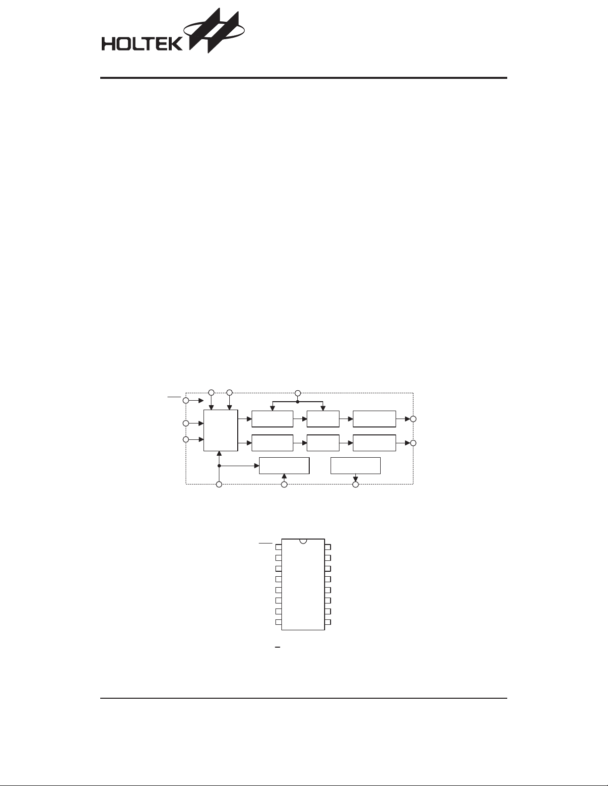
Block Diagram
L R C K
S D A T A
Pin Assignment
R S T
D I F 0 D I F 1 M C L K
S e r i a l
I n p u t
I n t e r f a c e
I n t e r p o l a t i o n
I n t e r p o l a t i o n
R S T
S D A T A
S C L K / D E M 1
L R C K
M C L K
D I F 1
D I F 0
D E M 0
F i l t e r
F i l t e r
D e - e m p h a s i s
D E M 0 M U T E CS C L K / D E M 1
1
2
3
4
5
6
7
8
H T 8 2 V 7 3 8
1 6 N S O P - A
D S
D S
1 6
1 5
1 4
1 3
1 2
1 1
1 0
D A C
D A C
9
A n a l o g F i l t e r
A n a l o g F i l t e r A O U T L
E x t e r n a l
M u t e C o n t r o l
M U T E C
A O U T A
V A
A G N D
A O U T B
R E F _ G N D
V Q
F I L T +
A O U T R
Rev. 1.00 1 October 16, 2003
Pin Description
Pin
No.
6, 7 DIF1, DIF0 I
Pin Name I/O Description
1 RST
2 SDATA I Serial data
3 SCLK/DEM1 I Serial clock/de-emphasis
4 LRCK I Left/right clock
5 MCLK I
I Reset
Master clock
Sample
Rate
(kHz)
32 4.0960 6.1440 8.1920 12.2880 16.3840
44.1 5.6448 8.4672 11.2896 16.9344 22.5792
48 6.1440 9.2160 12.2880 18.4320 24.5760
64 8.1920 12.2880
88.2 11.2896 16.9344
96 12.2880 18.4320
Digital interface format
DIF1 DIF0 Description
00I
0 1 Left justified, up to 24-bit data
1 0 Right justified, 24-bit data
1 1 Right justified, 16-bit data
128x 192x 256x 384x 512x
MCLK (MHz)
HRM BRM
¾¾¾
¾¾¾
¾¾¾
2
S, up to 24-bit data
HT82V738
De-emphasis control DEM0 and DEM1
Internal serial clock mode
DEM1 DEM0 Description
0 0 Disabled
0 1 44.1kHz
1 0 48kHz
8 DEM0 I
9 FILT+ I Positive voltage reference
10 VQ I Quiescent voltage
11 REF_GND I Reference ground
12 AOUTB O Analog output B
13 AGND I Analog ground
14 VA I Analog power
15 AOUTA O Analog output A
16 MUTEC O Mute control
1 1 32kHz
External serial clock mode
DEM0 Description
0 Disabled
1 44.1kHz
Rev. 1.00 2 October 16, 2003
HT82V738
Absolute Maximum Ratings
Supply Voltage ..........................VSS-0.3V to VSS+6.0V
Input Voltage .............................V
3V to VDD+0.3V
SS-0.
Note: These are stress ratings only. Stresses exceeding the range specified under ²Absolute Maximum Ratings² may
cause substantial damage to the device. Functional operation of this device at other conditions beyond those
listed in the specification is not implied and prolonged exposure to extreme conditions may affect device reliabil
ity.
Electrical Characteristics
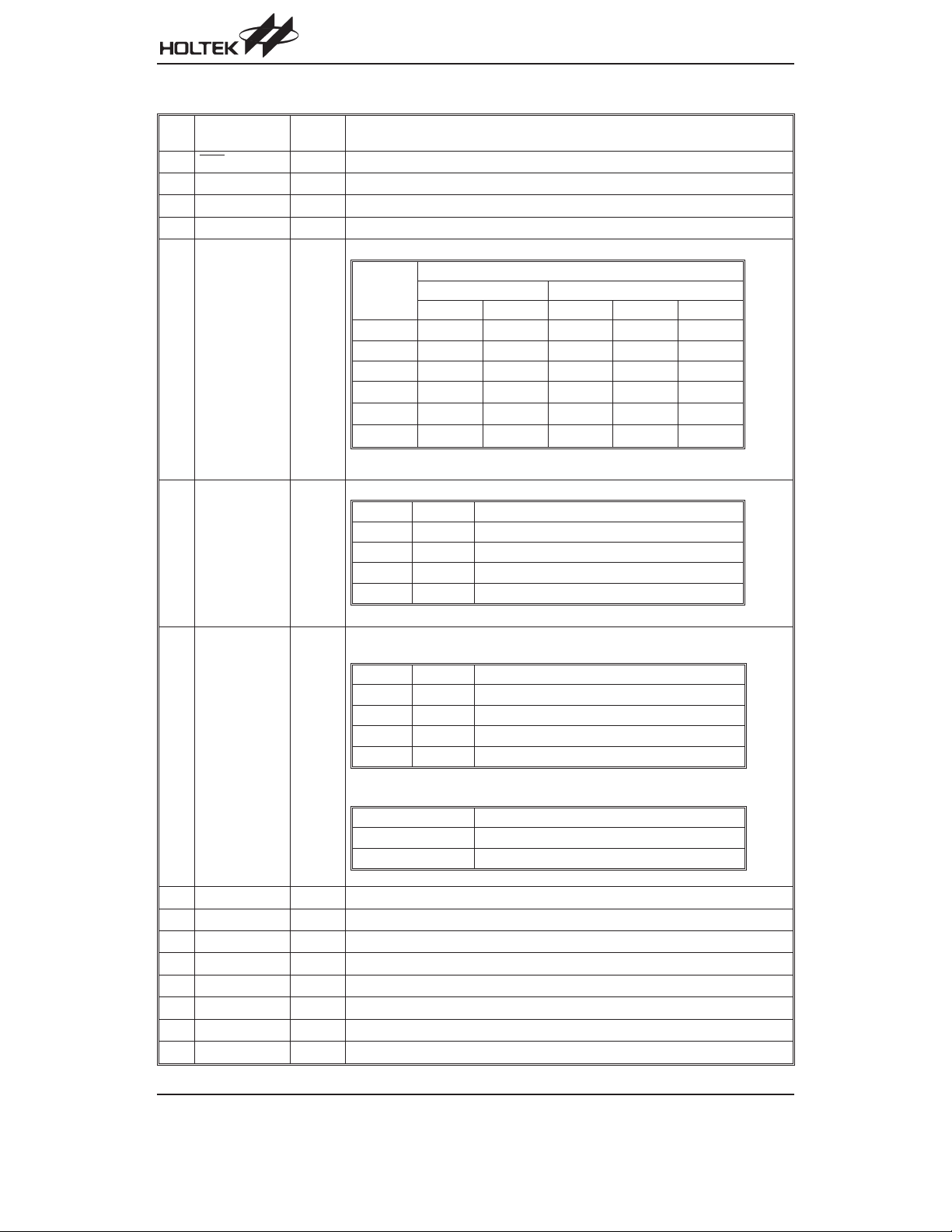
Analog Characteristics
Symbol Parameter
Dynamic Performance
Dynamic Range (18~24-bit)
Dynamic Range (16-bit)
Total Harmonic
Distortion+Noise
THD+N
(18~24-bit)
Total Harmonic
Distortion+Noise (16-bit)
Interchannel Isolation 5V
Dynamic Performance
Dynamic Range (18~24-bit)
Dynamic Range (16-bit)
Total Harmonic
THD+N
Distortion+Noise (18~24-bit)
Total Harmonic
Distortion+Noise (16-bit)
Interchannel Isolation 3V
Test Conditions Base-rate Mode High-rate Mode
V
Conditions Min. Typ. Max. Min. Typ. Max.
DD
Unweighted
A-weighted
5V
Unweighted
A-weighted
5V
Unweighted
A-weighted
3V
Unweighted
A-weighted
3V
Storage Temperature ...........................-50°Cto125°C
Operating Temperature ..........................-10°Cto70°C
Ta =-10°Cto70°C
93
¾
¾
¾
¾
95
91
94
¾¾
¾¾
¾¾
¾¾
92
95
88
94
¾
¾
¾
¾
¾¾-88 ¾¾-88 ¾
¾¾-86 ¾¾-86 ¾
¾¾90¾¾
91
¾
¾
¾
¾
94
90
92
¾¾
¾¾
¾¾
¾¾
90
90
91
88
90
¾
¾
¾
¾
¾
¾ ¾ -88 ¾ ¾ -88 ¾
¾ ¾ -86 ¾ ¾ -86 ¾
¾¾90¾¾
90
¾
Unit
dB
dB
dB
dB
dB
dB
-
Analog Characteristics
Symbol Parameter
Test Conditions
V
DD
Conditions
Min. Typ. Max. Unit
Analog Output
Full Scale Output Voltage
V
Quiescent Voltage
Q
Interchannel Gain Mismatch
Gain Drift
R
C
AC-load Resistance
L
Load Capacitance
L
¾¾ ¾
¾¾ ¾
¾¾ ¾
¾¾ ¾
¾¾
¾¾ ¾¾
0.7VA
0.5VA
0.1
100
3
¾¾kW
¾
¾
¾
¾ ppm/°C
100 pF
V
PP
VDC
dB
Rev. 1.00 3 October 16, 2003

HT82V738
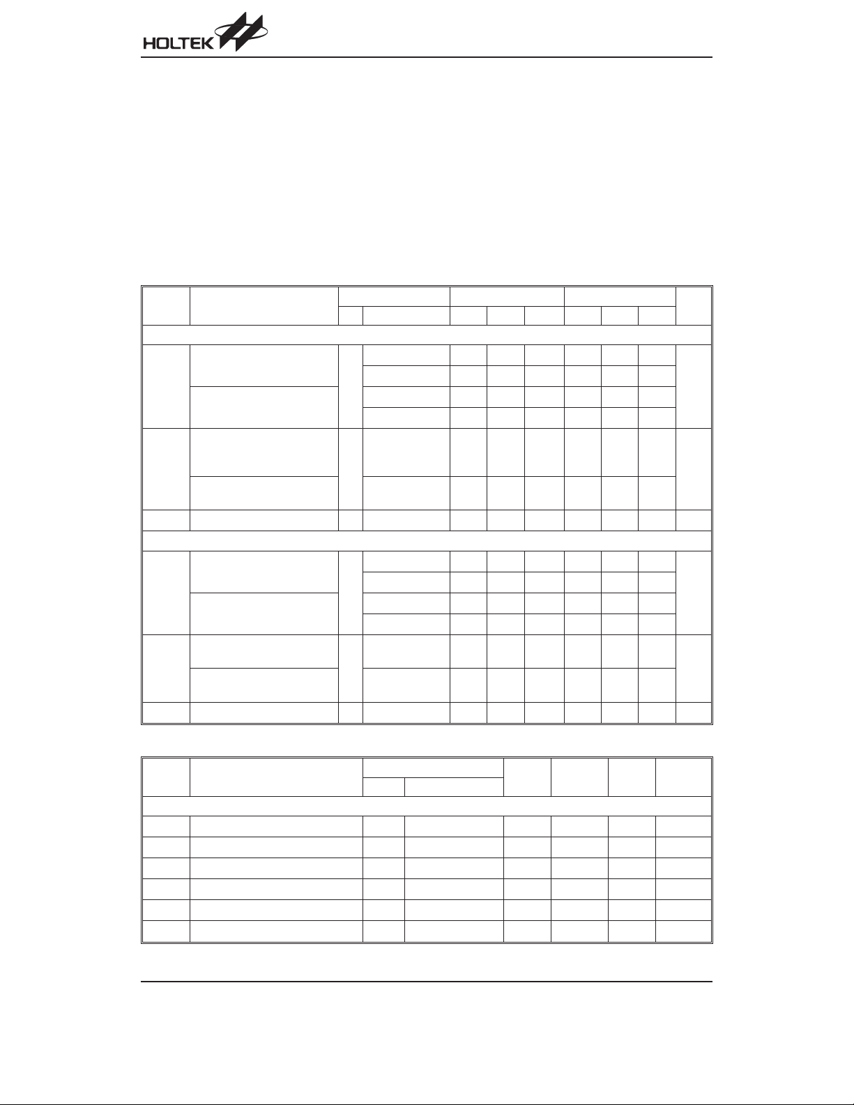
Digital Characteristics
Symbol Parameter
V
IH
V
IL
I
IN
High-level Input Voltage 5V
Low-level Input Voltage
Input Leakage Current
Input Capacitance
Power Ratio
V
A
V
IND
DC Power Supply
Digital Input Voltage
Power Characteristics
Symbol Parameter
I
A
I
A
Power Supply Current 3V Normal
Power Dissipation
Ta =-10°Cto70°C
V
DD
3V
5V
3V
Test Conditions
Conditions
¾
¾
¾¾¾
Min. Typ. Max. Unit
2.0
2.0
¾¾
¾¾
0.8 V
¾¾ ¾¾±10 mA
¾¾ ¾8¾
¾¾
¾¾ -0.3 ¾
2.7 5.0 5.5 V
+0.4
V
A
Test Conditions Base-rate Mode High-rate Mode
V
Conditions Min. Typ. Max. Min. Typ. Max.
DD
Power-down
Normal
5V
Power-down
Normal
3V
Power-down
Normal
5V
Power-down
10
¾
¾
¾
¾
¾
0.09
¾
¾
¾
30
15
60
30
75
0.3
¾¾
¾¾
¾¾
¾¾
¾¾
¾¾
¾¾
¾¾
10
30
15
60
30
0.09
75
0.3
¾
¾mA
¾
¾mA
¾
¾
¾
¾
V
V
pF
mA
Unit
mA
mA
mW
mW
Timing Diagrams
I2S Mode
·
16-bit data and INT SCLK=32Fs, MCLK/LRCK=512, 256 or 128
·
Up to 24-bit data and SCLK=48Fs, MCLK/LRCK=384 or 192
L R C K
S C L K
S D A T A
M S B
- 1 - 2 - 3 - 4 - 5 + 5 + 4 + 3 + 2
L S B
+ 1
M S B
- 2
- 1
- 3
Left Justified 24-Bit Mode
·
INT SCLK=64Fs, MCLK/LRCK=512, 256 or 128
·
INT SCLK=48Fs, MCLK/LRCK=384 or 192
L R C K
S C L K
S D A T A
M S B
- 1 - 2 - 3 - 4 - 5 + 5 + 4 + 3 + 2
L S B
+ 1
M S B
- 2
- 1
- 3
Rev. 1.00 4 October 16, 2003
R i g h t C h a n n e lL e f t C h a n n e l
- 4
+ 5
+ 4
R i g h t C h a n n e lL e f t C h a n n e l
- 4
+ 5
+ 4
L S B
+ 1
+ 3
+ 2
L S B
+ 1
+ 3
+ 2

Right Justified 24-Bit Mode
·
INT SCLK=64Fs, MCLK/LRCK=512, 256 or 128
·
INT SCLK=48Fs, MCLK/LRCK=384 or 192
HT82V738
L R C K
S C L K
S D A T A
0
2 3 2 2 2 1 2 0 1 9 1 8
7 6 5 4 3 2 1 0
Right Justified 16-Bit Mode
·
INT SCLK=32Fs, MCLK/LRCK=512, 256 or 128
·
INT SCLK=48Fs, MCLK/LRCK=384 or 192
L R C K
S C L K
S D A T A
7 6 5 4 3 2 1 0 1 3 1 2 1 1 1 0 9 8
81 01 11 21 31 41 5 9
Application Circuits
1 4
V A
6
D I F 1
M o d e
C o n f i g u r a t i o n
E x t e r n a l C l o c k
A u d i o
D a t a
P r o c e s s o r
7
8
1
5
2
3
4
D I F 0
D E M 0
R S T
M C L K
H T 8 2 V 7 3 8
S D A T A
S C L K / D E M 1
L R C K
R E F _ G N D
A G N D
1 3
0 . 1mF 1mF
F I L T +
1 0
V Q
1 1
A O U T A
A O U T B
1 6
1 5
1 2
M U T E C
R i g h t C h a n n e lL e f t C h a n n e l
2 3 2 2 2 1 2 0 1 9 1 8
R i g h t C h a n n e lL e f t C h a n n e l
1 41 5
+ 5 V t o + 3 V
+
7 6 5 4 3 2 1 0
7 6 5 4 3 2 1 0
9
0 . 1mF 1mF
1mF
0 . 1mF
3 . 3mF
3 . 3mF
5 6 0
W
1 0 k
5 6 0
1 0 k
C
W
W
C
W
O p t i o n a l
M u t e
C i r c u i t
1
C =
4pF s ( R
| | 5 6 0 )
L
R
L
R
L
A u d i o
O u t p u t A
A u d i o
O u t p u t B
Rev. 1.00 5 October 16, 2003

Package Information
16-pin NSOP (150mil) Outline Dimensions
HT82V738
1 6
A
1
C
D
E
Symbol
A 228
B 149
C14
C¢
D53
E
F4
G22
H4
9
B
8
C '
F
G
H
a
Dimensions in mil
Min. Nom. Max.
¾
¾
¾
386
¾
¾
¾
50
¾
¾
¾
a 0°¾10°
244
157
20
394
69
¾
10
28
12
Rev. 1.00 6 October 16, 2003

Product Tape and Reel Specifications
Reel Dimensions
HT82V738
T 2
A
B
T 1
D
SOP 16N (150mil)
Symbol Description Dimensions in mm
A Reel Outer Diameter
B Reel Inner Diameter
C Spindle Hole Diameter
D Key Slit Width
T1 Space Between Flange
T2 Reel Thickness
330±1.0
62±1.5
13.0+0.5
2.0±0.5
16.8+0.3
22.2±0.2
C
-0.2
-0.2
Rev. 1.00 7 October 16, 2003

Carrier Tape Dimensions
HT82V738
D
E
F
PD 1
P 1P 0
W
A 0
B 0
C
SOP 16N (150mil)
Symbol Description Dimensions in mm
W Carrier Tape Width
P Cavity Pitch
E Perforation Position
F Cavity to Perforation (Width Direction)
16.0±0.3
8.0±0.1
1.75±0.1
7.5±0.1
D Perforation Diameter 1.55+0.1
D1 Cavity Hole Diameter 1.5+0.25
P0 Perforation Pitch
P1 Cavity to Perforation (Length Direction)
A0 Cavity Length
B0 Cavity Width
K0 Cavity Depth
t Carrier Tape Thickness
4.0±0.1
2.0±0.1
6.5±0.1
10.3±0.1
2.1±0.1
0.3±0.05
C Cover Tape Width 13.3
t
K 0
Rev. 1.00 8 October 16, 2003

Holtek Semiconductor Inc. (Headquarters)
No.3, Creation Rd. II, Science Park, Hsinchu, Taiwan
Tel: 886-3-563-1999
Fax: 886-3-563-1189
http://www.holtek.com.tw
Holtek Semiconductor Inc. (Taipei Sales Office)
4F-2, No. 3-2, YuanQu St., Nankang Software Park, Taipei 115, Taiwan
Tel: 886-2-2655-7070
Fax: 886-2-2655-7373
Fax: 886-2-2655-7383 (International sales hotline)
HT82V738
Holtek Semiconductor Inc. (Shanghai Sales Office)
7th Floor, Building 2, No.889, Yi Shan Rd., Shanghai, China 200233
Tel: 021-6485-5560
Fax: 021-6485-0313
http://www.holtek.com.cn
Holtek Semiconductor Inc. (Shenzhen Sales Office)
5/F, Unit A, Productivity Building, Cross of Science M 3rd Road and Gaoxin M 2nd Road, Science Park, Nanshan District,
Shenzhen, China 518057
Tel: 0755-8616-9908, 8616-9308
Fax: 0755-8616-9533
Holtek Semiconductor Inc. (Beijing Sales Office)
Suite 1721, Jinyu Tower, A129 West Xuan Wu Men Street, Xicheng District, Beijing, China 100031
Tel: 010-6641-0030, 6641-7751, 6641-7752
Fax: 010-6641-0125
Holtek Semiconductor Inc. (Chengdu Sales Office)
709, Building 3, Champagne Plaza, No.97 Dongda Street, Chengdu, Sichuan, China 610016
Tel: 028-6653-6590
Fax: 028-6653-6591
Holmate Semiconductor, Inc. (North America Sales Office)
46729 Fremont Blvd., Fremont, CA 94538
Tel: 510-252-9880
Fax: 510-252-9885
http://www.holmate.com
Copyright Ó 2003 by HOLTEK SEMICONDUCTOR INC.
The information appearing in this Data Sheet is believed to be accurate at the time of publication. However, Holtek as
sumes no responsibility arising from the use of the specifications described. The applications mentioned herein are used
solely for the purpose of illustration and Holtek makes no warranty or representation that such applications will be suitable
without further modification, nor recommends the use of its products for application that may present a risk to human life
due to malfunction or otherwise. Holtek¢s products are not authorized for use as critical components in life support devices
or systems. Holtek reserves the right to alter its products without prior notification. For the most up-to-date information,
please visit our web site at http://www.holtek.com.tw.
-
Rev. 1.00 9 October 16, 2003
 Loading...