

16-Bit Stereo Audio D/A Converter
Features
·
Wide supply voltage range: 2.4V~5.5V
·
CMOS technology
·
Low power consumption
·
Two voltage output channel in the same chip
Applications
·
CD ROM/VCD
·
MP3/PDA/Smartphone
·
Digital portable audio equipment
General Description
HT82V731 is a 16-bit digital-to-analog converter IC uti
lizing CMOS technology specially designed for stereo
audio application. It converts the 16 bits serial data into
an analog output voltage by high precision D/A con
verter.
With its excellent frequency response characteristics,
the HT82V731 provides users a low cost means of im-
HT82V731
·
16-bit dynamic range
·
Low total harmonic distortion
·
Data in 2¢s complement format, TTL
·
8-pin SOP package
·
Satellite/cable STB
·
Motherboard/MPEG card
plementing high quality audio voltage outputs. Besides,
its wide supply voltage range from 2.4V to 5.5V makes
the device also suitable for use in battery-powered sys
tems or in application areas with low current consump
tion requirements. It is compatible with TDA1311 and
available in 8-pin SOP package.
-
-
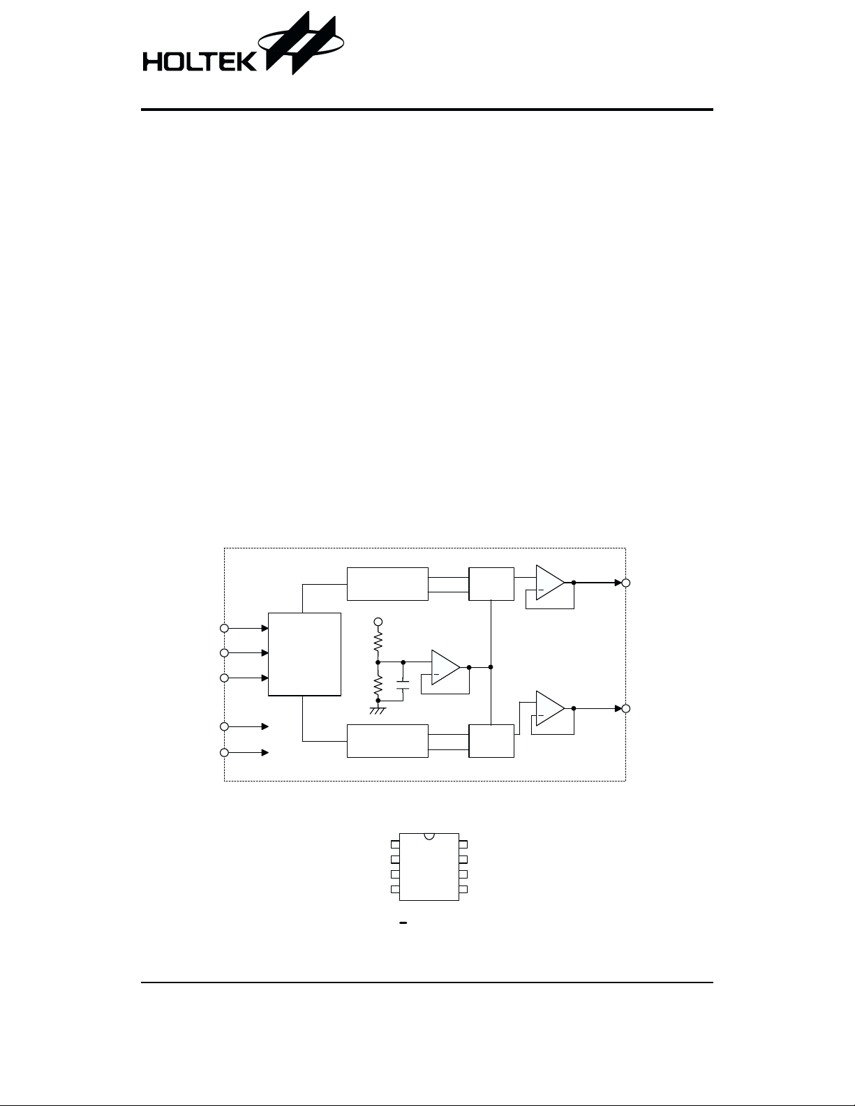
Block Diagram
B C K
W S
D I N
V D D
V S S
Pin Assignment
D a t a L a t c h
S e r i a l - t o - p a r a l l e l
C o n v e r s i o n
V
D D
S e r i a l - t o - p a r a l l e l
C o n v e r s i o n
B C K
1
W S
2
D I N
3
V S S
4
H T 8 2 V 7 3 1
8 S O P - A
O u t
+
D A C
O u t
+
o p
D A C
R C H
8
N C
7
L C H
6
V D D
5
o p
O u t
+
o p
R C H
L C H
Rev. 1.10 1 March 4, 2003
Pin Description
Pin No. Pin Name I/O Description
1
2
3
4
5
6
7
8
BCK
WS
DIN
VSS
VDD
LCH
NC
RCH
I Bit serial clock input
I Word select input
I Data input
Negative power supply, ground
¾
Positive power supply
¾
O Left channel output
No connection
¾
O Right channel output
HT82V731
Electrical Characteristics
Symbol Parameter
V
I
V
f
f
DD
DD
O
BCK
WS
Supply Voltage
Supply Current 5V
Maximum Output Amplitude 5V
Bit Clock Input Frequency
Word Select Input Frequency
THD Total Harmonic Distortion 5V 1kHz, 0dB*
DR Dynamic Range 5V
S/N Signal to Noise Ratio 5V
Note: ²*² means measured with 1kHz sinewave generated at a sampling rate of 192kHz.
Test Conditions
DD
Conditions
V
¾¾
Min. Typ. Max. Unit
2.4 5.0 5.5 V
¾¾¾
¾¾
¾¾ ¾¾
¾¾ ¾¾
¾
¾
¾¾16¾
A weighted at DIN
code=0000H
¾
Timing Diagrams
W S
R i g h t L e f t
tht
r
ft
2.5
65
0.055
92
Ta=25°C
6.0 mA
¾
Vpp
18.4 MHz
300 kHz
¾
¾
dB
%
Bit
¾
dB
B C K
D A T A
L S B + 1 M S B - 1
L S B M S B
S a m p l e O u t
Timing and input signals
Rev. 1.10 2 March 4, 2003
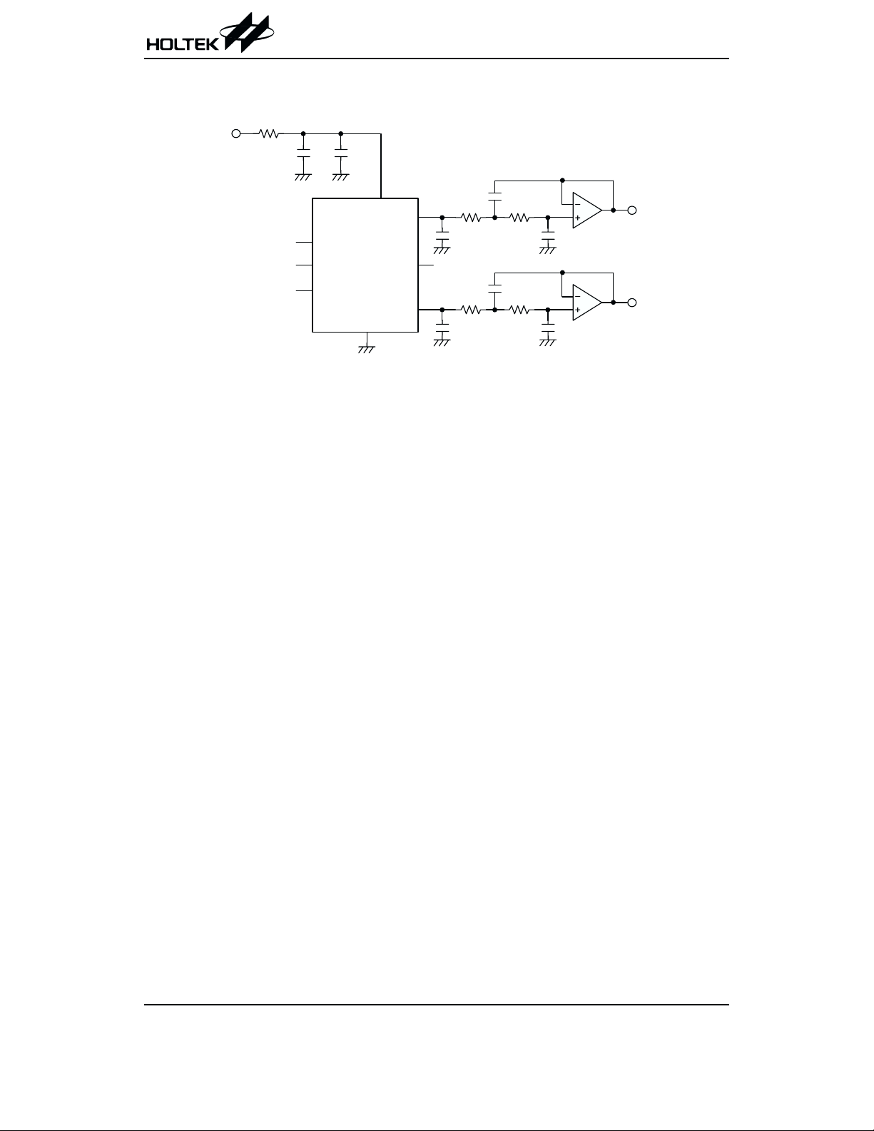
Application Circuits
V
1 0
D D
HT82V731
W
+
+
1 0 0 n F
F
4 7
m
1
2
3
B C K
W S
H T 8 2 V 7 3 1
D A T A
V S S
2 2 k
2 . 2 n F
2 2 k
2 . 2 n F
4 2 0 p F
W
4 2 0 p F
W
3
2 2 k
W
1 0 0 p F
2 2 k
W
1 0 0 p F
1
2
5
7
6
5
V D D
4
R C H
L C H
8
7
N C
6
Rev. 1.10 3 March 4, 2003

Package Information
8-pin SOP (150mil) Outline Dimensions
5
8
A
1
B
4
C
HT82V731
C '
D
E
F
Symbol
Min. Nom. Max.
A 228
B 149
C14
C¢
189
D53
E
¾
F4
G22
H4
G
H
a
Dimensions in mil
¾
¾
¾
¾
¾
50
¾
¾
¾
a 0°¾10°
244
157
20
197
69
¾
10
28
12
Rev. 1.10 4 March 4, 2003

Product Tape and Reel Specifications
Reel Dimensions
HT82V731
T 2
A
B
T 1
D
SOP 8N
Symbol Description Dimensions in mm
A Reel Outer Diameter
B Reel Inner Diameter
C Spindle Hole Diameter
D Key Slit Width
T1 Space Between Flange
T2 Reel Thickness
330±1.0
62±1.5
13.0+0.5
2.0±0.15
12.8+0.3
18.2±0.2
C
-0.2
-0.2
Rev. 1.10 5 March 4, 2003

Carrier Tape Dimensions
HT82V731
D
E
F
PD 1
P 1P 0
W
A 0
B 0
C
SOP 8N
Symbol Description Dimensions in mm
W Carrier Tape Width
P Cavity Pitch
E Perforation Position
F Cavity to Perforation (Width Direction)
D Perforation Diameter
12.0+0.3
8.0±0.1
1.75±0.1
5.5±0.1
1.55±0.1
D1 Cavity Hole Diameter 1.5+0.25
P0 Perforation Pitch
P1 Cavity to Perforation (Length Direction)
A0 Cavity Length
B0 Cavity Width
K0 Cavity Depth
t Carrier Tape Thickness
4.0±0.1
2.0±0.1
6.4±0.1
5.20±0.1
2.1±0.1
0.3±0.05
C Cover Tape Width 9.3
t
K 0
-0.1
Rev. 1.10 6 March 4, 2003

HT82V731
Holtek Semiconductor Inc. (Headquarters)
No.3, Creation Rd. II, Science-based Industrial Park, Hsinchu, Taiwan
Tel: 886-3-563-1999
Fax: 886-3-563-1189
http://www.holtek.com.tw
Holtek Semiconductor Inc. (Sales Office)
11F, No.576, Sec.7 Chung Hsiao E. Rd., Taipei, Taiwan
Tel: 886-2-2782-9635
Fax: 886-2-2782-9636
Fax: 886-2-2782-7128 (International sales hotline)
Holtek Semiconductor (Shanghai) Inc.
7th Floor, Building 2, No.889, Yi Shan Rd., Shanghai, China
Tel: 021-6485-5560
Fax: 021-6485-0313
http://www.holtek.com.cn
Holtek Semiconductor (Hong Kong) Ltd.
RM.711, Tower 2, Cheung Sha Wan Plaza, 833 Cheung Sha Wan Rd., Kowloon, Hong Kong
Tel: 852-2-745-8288
Fax: 852-2-742-8657
Holmate Semiconductor, Inc.
46712 Fremont Blvd., Fremont, CA 94538
Tel: 510-252-9880
Fax: 510-252-9885
http://www.holmate.com
Copyright Ó 2003 by HOLTEK SEMICONDUCTOR INC.
The information appearing in this Data Sheet is believed to be accurate at the time of publication. However, Holtek as
sumes no responsibility arising from the use of the specifications described. The applications mentioned herein are used
solely for the purpose of illustration and Holtek makes no warranty or representation that such applications will be suitable
without further modification, nor recommends the use of its products for application that may present a risk to human life
due to malfunction or otherwise. Holtek¢s products are not authorized for use as critical components in life support devices
or systems. Holtek reserves the right to alter its products without prior notification. For the most up-to-date information,
please visit our web site at http://www.holtek.com.tw.
-
Rev. 1.10 7 March 4, 2003
 Loading...