

查询HT7130供应商
Features
Low power consumption
·
Low voltage drop
·
Low temperature coefficient
·
Applications
Battery-powered equipment
·
Communication equipment
·
General Description
The HT71XX series is a set of three-terminal
low power high voltage regulators implemented
in CMOS technology. They allow input voltages
as high as 24V. They are available with several
fixed output voltages ranging from 3.0V to
5.0V. CMOS technology ensures low voltage
drop and low quiescent current.
HT71XX
High Voltage Regulator
High input voltage (up to 24V)
·
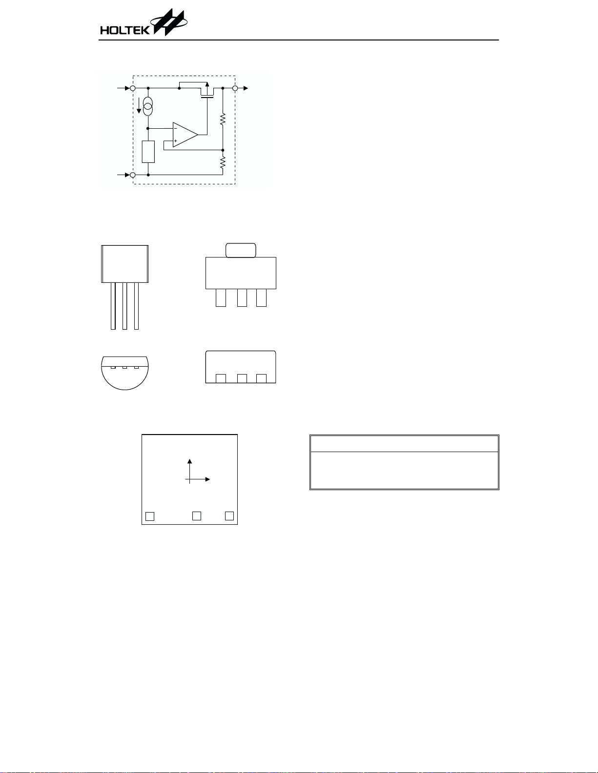
TO-92 and SOT-89 packages
·
Audio/Video equipment
·
Although designed primarily as fixed voltage
regulators, these devices can be used with ex
ternal components to obtain variable voltages
and currents.
-
Selection Table
Part No. Output Voltage Tolerance
HT7130 3.0V
HT7133 3.3V
HT7136 3.6V
HT7144 4.4V
HT7150 5.0V
±5%
±5%
±5%
±5%
±5%
1 August 8, 2000
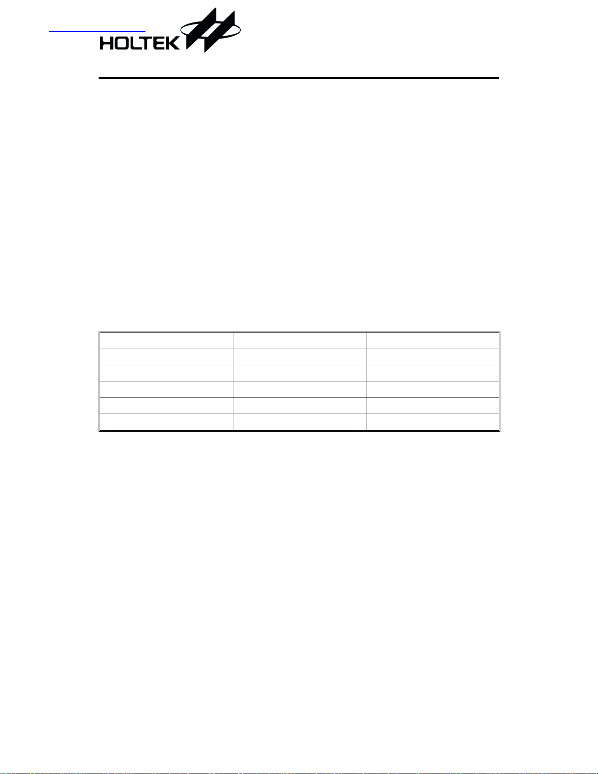
Block Diagram
V
ref
GND
Pin Assignment
HT71XX
VOUTVIN
TO -92
HT71XXA
Front View
SO T-89
HT71XX
VOUTGND
VIN
Bottom View
GND
VIN
VOUT
Pad Assignment Pad Coordinates
Pad No. X Y
1
(0 ,0 )
2 87.50
3 482.00
1
GND
2 3
VIN
VOUT
-480.00 -451.50
Unit: mm
-444.50
-444.50
Chip size: 1374´1294 (mm)
2
* The IC substrate should be connected to VDD in the PCB layout artwork.
2 August 8, 2000
Absolute Maximum Ratings
HT71XX
Supply Voltage ..............................-0.3V to 28V
Power Consumption ............................. 200mW
Storage Temperature ................-50°Cto125°C
Operating Temperature .................0°Cto70°C
Note: These are stress ratings only. Stresses exceeding the range specified under Absolute Maxi
mum Ratings may cause substantial damage to the device. Functional operation of this de
vice at other conditions beyond those listed in the specification is not implied and prolonged
exposure to extreme conditions may affect device reliability.
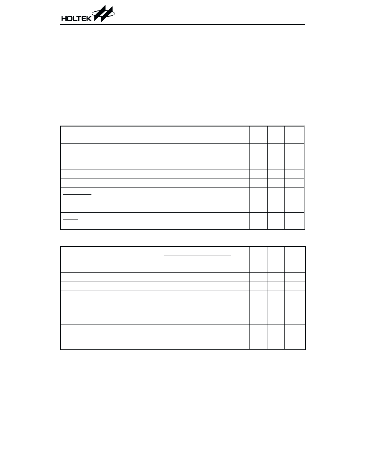
Electrical Characteristics
HT7130, +3.0V output type
Symbol Parameter
V
OUT
I
OUT
DV
OUT
V
DIF
I
SS
DDV
OUT
´
VV
IN OUT
V
IN
DDV
OUT
T
a
Output Voltage 5V I
Output Current 5V
Load Regulation 5V
Voltage Drop
Current Consumption 5V No load
Line Regulation
Input Voltage
Temperature Coefficient 5V
Test Conditions
V
IN
Conditions
=10mA 2.85 3.0 3.15 V
OUT
1mA£I
=1mA
I
¾
OUT
4V£V
I
OUT
IN
=1mA
¾
¾
£20mA ¾
OUT
£24V
Min. Typ. Max. Unit
20 30
60 100 mV
100
¾
¾
¾
4 6.0
0.2
¾¾ ¾¾
I
=10mA
OUT
0°C<Ta<70°C
¾±0.45 ¾ mV/°C
Ta=25°C
mA
¾
mV
¾
mA
%/V
¾
24 V
-
-
HT7133, +3.3V output type
Symbol Parameter
V
OUT
I
OUT
DV
OUT
V
DIF
I
SS
DDV
OUT
´
VV
IN OUT
V
IN
DDV
OUT
T
a
Output Voltage 5.5V I
Output Current 5.5V
Load Regulation 5.5V
Voltage Drop
Current Consumption 5.5V No load
Line Regulation
Input Voltage
Temperature Coefficient 5.5V
Test Conditions
V
IN
Conditions
=10mA 3.135 3.3 3.465 V
OUT
¾
£30mA ¾
OUT
=1mA
£24V
IN
=1mA
¾
¾
1mA£I
I
OUT
4.5V£V
I
OUT
¾¾ ¾¾
I
=10mA
OUT
0°C<Ta<70°C
3 August 8, 2000
Min. Typ. Max. Unit
20 30
¾
60 100 mV
100
¾
¾
¾
0.2
¾
46
¾
24 V
¾±0.5 ¾ mV/°C
Ta=25°C
mA
mV
mA
%/V

HT71XX
HT7136, +3.6V output type
Symbol Parameter
V
OUT
I
OUT
DV
OUT
V
DIF
I
SS
DDV
OUT
´
VV
IN OUT
V
IN
DDV
OUT
T
a
Output Voltage 5.6V I
Output Current 5.6V
Load Regulation 5.6V
Voltage Drop
Current Consumption 5.6V No load
Line Regulation
Input Voltage
Temperature Coefficient 5.6V
HT7144, +4.4V output type
Symbol Parameter
V
OUT
I
OUT
DV
OUT
V
DIF
I
SS
DDV
OUT
´
VV
IN OUT
V
IN
DDV
OUT
T
a
Output Voltage 6.4V I
Output Current 6.4V
Load Regulation 6.4V
Voltage Drop
Current Consumption 6.4V No load
Line Regulation
Input Voltage
Temperature Coefficient 6.4V
Test Conditions
Min. Typ. Max. Unit
V
IN
¾
¾
¾¾ ¾¾
Conditions
=10mA 3.42 3.6 3.78 V
OUT
¾
1mA£I
I
OUT
4.6V£V
I
OUT
I
OUT
£30mA ¾
OUT
=1mA
£12V
IN
=1mA
=10mA
0°C<Ta<70°C
20 30
60 100 mV
¾
¾
¾
60
3.0 7.0
0.2
¾±0.6 ¾ mV/°C
¾
¾
¾
24 V
Test Conditions
Min. Typ. Max. Unit
V
IN
¾
¾
¾¾ ¾¾
Conditions
=10mA 4.18 4.4 4.62 V
OUT
¾
1mA£I
I
OUT
5.4V£V
I
OUT
I
OUT
£30mA ¾
OUT
=1mA
£24V
IN
=1mA
=10mA
0°C<Ta<70°C
20 30
60 100 mV
100
¾
¾
¾
4 7.5
0.2
¾±0.7 ¾ mV/°C
¾
¾
¾
24 V
Ta=25°C
mA
mV
mA
%/V
Ta=25°C
mA
mV
mA
%/V
4 August 8, 2000

HT71XX
HT7150, +5.0V output type
Symbol Parameter
V
OUT
I
OUT
DV
OUT
V
DIF
I
SS
DDV
OUT
´
VV
IN OUT
V
IN
DDV
OUT
T
a
Output Voltage 7V I
Output Current 7V
Load Regulation 7V
Voltage Drop
Current Consumption 7V No load
Line Regulation
Input Voltage
Temperature Coefficient 7V
Application Circuits
Basic circuits
V
IN
10mF
C1
Ta=25°C
Test Conditions
Min. Typ. Max. Unit
V
IN
¾
¾
¾¾ ¾¾
V
IN
HT71XX
GND
Conditions
=10mA 4.75 5.0 5.25 V
OUT
1mA£I
=1mA
I
OUT
6V£V
IN
I
=1mA
OUT
I
=10mA
OUT
0°C<Ta<70°C
Series
¾
£30mA ¾
OUT
£24V
V
OUT
20 30
60 100 mV
100
¾
¾
¾
59
0.2
¾±0.75 ¾ mV/°C
V
OUT
C2
10mF
mA
¾
mV
¾
mA
%/V
¾
24 V
Com m on Com m on
Single point G N D
5 August 8, 2000

High output current positive voltage regulator
Tr1
HT71XX
V
IN
R1
10mF
Com m on Com m on
Short-Circuit protection by Tr1
V
IN
Com m on Com m on
Rs
R1
10mF
C1
C1
Tr1
V
V
IN
HT71XX
V
OUT
OUT
Series
GND
C2
10mF
Single point G N D
V
V
IN
HT71XX
V
OUT
OUT
Series
GND
C2
10mF
Single point G N D
Circuit for increasing output voltage
V
IN
10mF
Com m on Com m on
C1
V
IN
V
HT71XX
OUT
Series
GND
I
SS
Single point G N D
VV(1+
=+
OUT XX SS
R2
)I R2
R1
6 August 8, 2000
C2
10mF
V
OUT
V
R1
XX
R2

Circuit for increasing output voltage
HT71XX
V
IN
10mF
Com m on Com m on
Constant current regulator
V
IN
C1
10mF
Com m on
C1
V
V
IN
HT71XX
V
OUT
OUT
Series
V
XX
GND
I
SS
C2
10mF
R1
D1
Single point G N D
V
OUT=VXX+VD1
V
IN
HT71XX
V
OUT
Series
GND
I
I
SS
V
=+
OUT
R
XX
A
V
C2
10mF
I
SS
R
XX
A
I
OUT
R
L
Dual supply
Com m on Com m on
IC 1
V
IN
IC 2
V
IN
HT71XX
Series
GND
V
OUT
V
OUT1
C3
10mF
10mF
C1
V
IN
HT71XX
Series
GND
V
OUT
V
OUT2
R1
C2
10mF
7 August 8, 2000

HT71XX
Holtek Semiconductor Inc. (Headquarters)
No.3 Creation Rd. II, Science-based Industrial Park, Hsinchu, Taiwan, R.O.C.
Tel: 886-3-563-1999
Fax: 886-3-563-1189
Holtek Semiconductor Inc. (Taipei Office)
5F, No.576, Sec.7 Chung Hsiao E. Rd., Taipei, Taiwan, R.O.C.
Tel: 886-2-2782-9635
Fax: 886-2-2782-9636
Fax: 886-2-2782-7128 (International sales hotline)
Holtek Semiconductor (Hong Kong) Ltd.
RM.711, Tower 2, Cheung Sha Wan Plaza, 833 Cheung Sha Wan Rd., Kowloon, Hong Kong
Tel: 852-2-745-8288
Fax: 852-2-742-8657
Copyright Ó 2000 by HOLTEK SEMICONDUCTOR INC.
The information appearing in this Data Sheet is believed to be accurate at the time of publication. However, Holtek
assumes no responsibility arising from the use of the specifications described.The applications mentioned herein are
used solely for the purpose of illustration and Holtek makes no warranty or representation that such applications
will be suitable without further modification, nor recommends the use of its products for application that may pres
ent a risk to human life due to malfunction or otherwise. Holtek reserves the right to alter its products without prior
notification. For the most up-to-date information, please visit our web site at http://www.holtek.com.tw.
8 August 8, 2000
-
 Loading...