

查询HT6P20A供应商
Features
·
Operating voltage: 2V~12V
·
Low power consumption
·
Built-in oscillator needs only 5% resistor
·
0/2/4/8 data selectable
·
224maximum address and data codes
·
Easy interface with an RF or IR medium
Applications
·
Burglar alarm system
·
Smoke and fire alarm system
·
Garage door controllers
·
Car door controllers
General Description
The HT6P20X is a CMOS LSI encoder designed for re
mote control system applications. It encodes 24 bits of
information and then serially transmits it via the DOUT
pin upon receipt of transmission enable (DATA pins:
D0~D7) signals. The combination of address and data
bits of the HT6P20X is designed using one time pro-
HT6P20X Series
224OTP Encoder
·
One time programmable process
·
Data active: D0~D7
·
Minimal external components
·
HT6P20A/B: 8-pin DIP/SOP package
HT6P20D: 16-pin DIP/NSOP package
·
Security system
·
Cordless telephones
·
Other remote control systems
grammable process. In addition, the chip offers various
packaging for flexible combination of programmable ad
dress/data so as to meet various applications. Its pro
grammable address/data is transmitted together with
the anti-code bits via RF or infrared transmission medium upon receipt of a trigger signal.
-
-
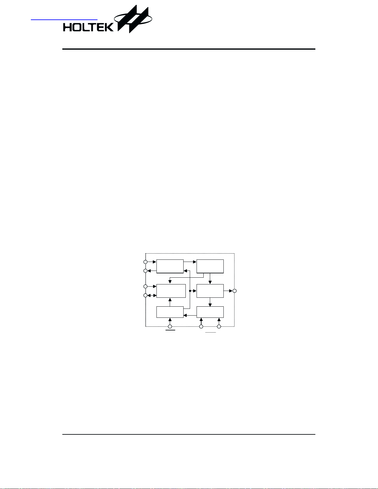
Block Diagram
O S C 1
O S C 2
V P P
S I O
O s c i l l a t o r
P r o g r a m m i n g
C i r c u i t
C o n t r o l U n i t
P G M
Note: Address/Data numbers are available in various combinations, refer to the functional description.
A d d r e s s
C o u n t e r
M i x e r &
D r i v e r
D a t a L a t c h
D 0 D 7
D O U T
Rev. 1.40 1 June 20, 2003
Pin Assignment
HT6P20X Series
2 4 - A d d r e s s
0 - D a t a
P G M
1
V S S
2
O S C 2
3
O S C 1
4
H T 6 P 2 0 A
8 D I P / S O P
S I O
8
V P P
7
V D D
6
D O U T
5
2 2 - A d d r e s s
2 - D a t a
D 0
1
D 1
2
V S S
3
O S C 2
4
H T 6 P 2 0 B
8 D I P / S O P
N C
8
V D D
7
D O U T
6
O S C 1
5
Pin Description
HT6P20D
I
Internal
Connection
CMOS IN
Pull-high
¾
CMOS
IN/OUT
CMOS IN
Pull-high
Data input and transmission enable (active low)
They can be externally set to VSS or left open.
Negative power supply, ground
No connection
Positive power supply
Programming power supply, V
Programming address/control code input and mode code output for
mode verification
Program mode control pin, active low
Pin No. Pin Name I/O
16
1~3
4 VSS
5~8 NC
D0~D3 I
¾¾
¾¾
9 OSC2 O OSCILLATOR Oscillator output pin
10 OSC1 I OSCILLATOR Oscillator input pin
11 DOUT O CMOS OUT Data serial transmission output
12 VDD
¾¾
13 VPP I
14 SIO I/O
15 PGM
2 0 - A d d r e s s
4 - D a t a
D 1
D 2
D 3
V S S
N C
N C
N C
N C
1 6 D I P / N S O P
Description
for normal operation
DD
1
2
3
4
5
6
7
8
H T 6 P 2 0 D
1 6
D 0
1 5
P G M
1 4
S I O
1 3
V P P
1 2
V D D
1 1
D O U T
1 0
O S C 1
9
O S C 2
Approximate internal connection circuits
C M O S I N / O U T
C M O S O U T
C M O S I N
P u l l - h i g h
V
D D
O S C 1
O S C I L L A T O R
O S C 2
Rev. 1.40 2 June 20, 2003
HT6P20X Series
Absolute Maximum Ratings
Supply Voltage ...........................VSS-0.3V to VSS+12V
Input Voltage..............................V
-0.3V to VDD+0.3V
SS
Note: These are stress ratings only. Stresses exceeding the range specified under ²Absolute Maximum Ratings² may
cause substantial damage to the device. Functional operation of this device at other conditions beyond those
listed in the specification is not implied and prolonged exposure to extreme conditions may affect device reliabil
ity.
Storage Temperature ............................-50°Cto125°C
Operating Temperature ...........................-20°Cto75°C
-
Electrical Characteristics
Symbol Parameter
V
DD
I
STB
I
DD
V
IH
V
IL
R
PH
I
DOUT
f
OSC
Operating Voltage
Standby Current 12V Oscillator stops
Operating Current 12V
²H² Input Voltage ¾¾
²L² Input Voltage ¾¾
D0~D7 Pull-high Resistance 12V
Output Current
Oscillator Frequency 12V
Source
Sink
Test Conditions
V
DD
Conditions
¾¾
No load, f
OSC
=3kHz
¾¾
0.9V
5V
12V
5V
12V
DD
0.9V
DD
0.1V
DD
0.1V
DD
=1.4MW¾
R
OSC
Min. Typ. Max. Unit
2
¾
¾
0.8V
0
DD
¾
12
200 400
¾
¾
V
0.2V
150 300
-2 -5 ¾
-6.5 -15 ¾
25
615
3
Ta=25°C
12 V
DD
DD
mA
mA
¾
¾
¾
mA
mA
kHz
mA
mA
V
V
kW
Functional Description
Normal Operation
The HT6P20X encodes and transmits address/data to a decoder upon receipt of a trigger signal. The address codes of
the HT6P20A are always transmitted as long as power (VDD) is supplied. The transmission function of the HT6P20B/D
is enabled by the D0~D7 pins (active low). The following is the transmission timing of the HT6P20X:
D 0 ~ D 7
E n c o d e r
D O U T
< 1 w o r d
> 1 w o r d
Transmission timing
A complete code word of the HT6P20D consists of 3 periods as shown below.
f o s c
D O U T
1 c l o c k
p i l o t p e r i o d
( 2 3 c l o c k s )
1 / 3 b i t
( A 0 ~ A 1 9 , 6 0 c l o c k s )
a d d r e s s c o d e p e r i o d
( D 3 ~ D 0 , 1 2 c l o c k s )
d a t a c o d e p e r i o d
0 01 1
a n t i - c o d e p e r i o d
( 4 b i t s )
A complete code word for the HT6P20D
Rev. 1.40 3 June 20, 2003
HT6P20X Series
The HT6P20A/B/D detects the logic state of the internal programmed address and the external data pins, and then trans
mits the detected information during the code period. Each address/data bit can be set to one of the following two logic
states:
f o s c
" O n e "
" Z e r o "
A d d r e s s /
D a t a b i t
Flowchart
P o w e r o n
S t a n d b y m o d e
N o
A d d r e s s / d a t a w o r d s
N o
T r a n s m i s s i o n
A d d r e s s / d a t a w o r d s
T r a n s m i s s i o n
e n a b l e d ?
Y e s
t r a n s m i t t e d
s t i l l e n a b l e d
Y e s
t r a n s m i t t e d
c o n t i n u o u s l y
N o
N o
N o t e : O n e t i m e p r o g r a m m a b l e
P G M = 0 ?
Y e s
P r o g r a m m i n g
m o d e
P r o g r a m m i n g
c o m p l e t e d ?
Y e s
-
Rev. 1.40 4 June 20, 2003

Application Circuits
HT6P20X Series
T r a n s m i t t e r C i r c u i t
R o s c
T r a n s m i t t e r C i r c u i t
1
P G M
2
V S S
3
O S C 2
4
O S C 1
D O U T
H T 6 P 2 0 A
R o s c@1 . 4 M
T r a n s m i t t e r C i r c u i t
1
2
D 2
3
D 3
4
V S S
5
N C
6
N C
7
N C
8
N C
P G M
D O U T
O S C 1
O S C 2
V P P
V D D
V P P
V D D
1
2
D 2
3
8
S I O
7
6
5
+ 1 2 V
T E
L E D
D 3
4
V S S
5
N C
6
N C
7
N C
8
N C
P G M
V P P
V D D
D O U T
O S C 1
O S C 2
1 6
D 0D 1
1 5
1 4
S I O
1 3
1 2
1 1
1 0
9
+ 1 2 V
L E D
R o s c
H T 6 P 2 0 D
W
1 6
D 0D 1
1 5
1 4
S I O
1 3
1 2
1 1
1 0
9
R o s c
+ 1 2 V
1 0 0
0 . 1mF
W
R o s c@1 . 4 M
W
H T 6 P 2 0 D
R o s c@1 . 4 M
Rev. 1.40 5 June 20, 2003
W

T r a n s m i t t e r C i r c u i t
+ 1 2 V
1 0 0 k
HT6P20X Series
W
4 . 7 k
W
T r a n s m i t t e r C i r c u i t
1
2
D 2
3
D 3
4
V S S
5
N C
6
N C
7
N C
8
N C
P G M
V D D
D O U T
O S C 1
O S C 2
1 6
D 0D 1
1 5
1 4
S I O
1 3
V P P
1 2
1 1
1 0
R o s c
9
1 0 0
0 . 1mF
+ 1 2 V
W
L E D
H T 6 P 2 0 D
R o s c@1 . 4 M
Note:
In order to prevent the IC from getting damaged due to the latch up, the 100W resistor or the LED which can
also be a transmission indicator is indispensible when V
W
=9V~12V.
DD
1
2
D 2
3
D 3
4
V S S
5
N C
6
N C
7
N C
8
N C
H T 6 P 2 0 D
R o s c@1 . 4 M
D 0D 1
P G M
S I O
V P P
V D D
D O U T
O S C 1
O S C 2
W
1 6
1 5
1 4
1 3
1 0 0
R o s c
0 . 1mF
W
L E D
1 2
1 1
1 0
9
Rev. 1.40 6 June 20, 2003

Package Information
8-pin DIP (300mil) Outline Dimensions
B
C
D
E
HT6P20X Series
A
8
5
4
1
H
I
G
F
a
Symbol
Min. Nom. Max.
A 355
B 240
C 125
D 125
E16
F50
G
¾
H 295
I 335
Dimensions in mil
¾
¾
¾
¾
¾
¾
100
¾
¾
a 0°¾15°
375
260
135
145
20
70
¾
315
375
Rev. 1.40 7 June 20, 2003

16-pin DIP (300mil) Outline Dimensions
HT6P20X Series
A
1 6
B
1
C
D
E
F
Symbol
A 745
B 240
C 125
D 125
E16
F50
G
H 295
I 335
9
8
H
G
a
I
Dimensions in mil
Min. Nom. Max.
¾
¾
¾
¾
¾
¾
¾
100
¾
¾
a 0°¾15°
775
260
135
145
20
70
¾
315
375
Rev. 1.40 8 June 20, 2003

8-pin SOP (150mil) Outline Dimensions
5
8
A
1
B
4
C
HT6P20X Series
C '
D
E
F
Symbol
Min. Nom. Max.
A 228
B 149
C14
C¢
189
D53
E
¾
F4
G22
H4
G
H
a
Dimensions in mil
¾
¾
¾
¾
¾
50
¾
¾
¾
a 0°¾10°
244
157
20
197
69
¾
10
28
12
Rev. 1.40 9 June 20, 2003

16-pin NSOP (150mil) Outline Dimensions
HT6P20X Series
1 6
A
1
C
D
E
Symbol
A 228
B 149
C14
C¢
D53
E
F4
G22
H4
9
B
8
C '
F
G
H
a
Dimensions in mil
Min. Nom. Max.
¾
¾
¾
386
¾
¾
¾
50
¾
¾
¾
a 0°¾10°
244
157
20
394
69
¾
10
28
12
Rev. 1.40 10 June 20, 2003

Product Tape and Reel Specifications
Reel Dimensions
HT6P20X Series
T 2
A
B
T 1
D
SOP 8N
Symbol Description Dimensions in mm
A Reel Outer Diameter
B Reel Inner Diameter
C Spindle Hole Diameter
D Key Slit Width
T1 Space Between Flange
T2 Reel Thickness
330±1.0
62±1.5
13.0+0.5
2.0±0.15
12.8+0.3
18.2±0.2
C
-0.2
-0.2
SOP 16N (150mil)
Symbol Description Dimensions in mm
A Reel Outer Diameter
B Reel Inner Diameter
C Spindle Hole Diameter
D Key Slit Width
T1 Space Between Flange
T2 Reel Thickness
330±1.0
62±1.5
13.0+0.5
-0.2
2.0±0.5
16.8+0.3
-0.2
22.2±0.2
Rev. 1.40 11 June 20, 2003

Carrier Tape Dimensions
HT6P20X Series
D
E
F
PD 1
P 1P 0
W
A 0
B 0
C
SOP 8N
Symbol Description Dimensions in mm
W Carrier Tape Width
P Cavity Pitch
E Perforation Position
F Cavity to Perforation (Width Direction)
D Perforation Diameter
12.0+0.3
8.0±0.1
1.75±0.1
5.5±0.1
1.55±0.1
D1 Cavity Hole Diameter 1.5+0.25
P0 Perforation Pitch
P1 Cavity to Perforation (Length Direction)
A0 Cavity Length
B0 Cavity Width
K0 Cavity Depth
t Carrier Tape Thickness
4.0±0.1
2.0±0.1
6.4±0.1
5.20±0.1
2.1±0.1
0.3±0.05
C Cover Tape Width 9.3
t
K 0
-0.1
NSOP 16N
Symbol Description Dimensions in mm
W Carrier Tape Width
P Cavity Pitch
E Perforation Position
F Cavity to Perforation (Width Direction)
16.0±0.3
8.0±0.1
1.75±0.1
7.5±0.1
D Perforation Diameter 1.55+0.1
D1 Cavity Hole Diameter 1.5+0.25
P0 Perforation Pitch
P1 Cavity to Perforation (Length Direction)
A0 Cavity Length
B0 Cavity Width
K0 Cavity Depth
t Carrier Tape Thickness
4.0±0.1
2.0±0.1
6.5±0.1
10.3±0.1
2.1±0.1
0.3±0.05
C Cover Tape Width 13.3
Rev. 1.40 12 June 20, 2003

Holtek Semiconductor Inc. (Headquarters)
No.3, Creation Rd. II, Science Park, Hsinchu, Taiwan
Tel: 886-3-563-1999
Fax: 886-3-563-1189
http://www.holtek.com.tw
HT6P20X Series
Holtek Semiconductor Inc. (Taipei Sales Office)
4F-2, No. 3-2, YuanQu St., Nankang Software Park, Taipei 115, Taiwan
Tel: 886-2-2655-7070
Fax: 886-2-2655-7373
Fax: 886-2-2655-7383 (International sales hotline)
Holtek Semiconductor Inc. (Shanghai Sales Office)
7th Floor, Building 2, No.889, Yi Shan Rd., Shanghai, China 200233
Tel: 021-6485-5560
Fax: 021-6485-0313
http://www.holtek.com.cn
Holtek Semiconductor Inc. (Shenzhen Sales Office)
43F, SEG Plaza, Shen Nan Zhong Road, Shenzhen, China 518031
Tel: 0755-8346-5589
Fax: 0755-8346-5590
ISDN: 0755-8346-5591
Holtek Semiconductor Inc. (Beijing Sales Office)
Suite 1721, Jinyu Tower, A129 West Xuan Wu Men Street, Xicheng District, Beijing, China 100031
Tel: 010-6641-0030, 6641-7751, 6641-7752
Fax: 010-6641-0125
Holmate Semiconductor, Inc. (North America Sales Office)
46712 Fremont Blvd., Fremont, CA 94538
Tel: 510-252-9880
Fax: 510-252-9885
http://www.holmate.com
Copyright Ó 2003 by HOLTEK SEMICONDUCTOR INC.
The information appearing in this Data Sheet is believed to be accurate at the time of publication. However, Holtek as
sumes no responsibility arising from the use of the specifications described. The applications mentioned herein are used
solely for the purpose of illustration and Holtek makes no warranty or representation that such applications will be suitable
without further modification, nor recommends the use of its products for application that may present a risk to human life
due to malfunction or otherwise. Holtek¢s products are not authorized for use as critical components in life support devices
or systems. Holtek reserves the right to alter its products without prior notification. For the most up-to-date information,
please visit our web site at http://www.holtek.com.tw.
-
Rev. 1.40 13 June 20, 2003
 Loading...