

Page 1
HT67F86A Internal RTC Application Guidelines
HT67F86A Internal RTC Application Guidelines
D/N: AN0448E
Introduction
One special feature of the Holtek 8-bit Flash MCU, the HT67F86A, is that it includes an
ultra-low power consumption RTC oscillator and an LCD driver. To meet the demands for
low power consumption applications, the device’s internal RTC has a standby power
consumption of lower than 1µA at an operating voltage of 3V. The integrated LCD driver
can drive dot matrix LCD display applications of up to 1024 pixels, which can be used with
various display configurations and font settings. With the increasing trends of mobile
device applications such as cellphones and tablets, in addition to being utilised in
industrial control and consumer products, the ultra-low standby power consumption
performance is also an especially important consideration in battery-powered applications.
The MCU’s internal RTC oscillator forms an excellent solution for applications which
require a real time clock function as it reduces the need for an external timing IC with the
resulting reductions in cost and design simplification. This application note will introduce
the Holtek MCU internal RTC oscillator characteristics and application guidelines.
Functional Description
Oscillators
The HT67F86A provides 3 frequency oscillation sources, namely the HXT, HITC and LXT
oscillators. Users can select their desired system frequency, f
program. The LXT provides an f
commonly for applications requiring an RTC real-time clock. Additionally, the MCU can
enter the IDLE2 or SLEEP power saving modes also using the application program to
implement different standby power consumption power down modes. The related
registers are listed in the following table, refer to the Oscillators section in the datasheet
for more detailed information.
Register
Name
SCC CKS2 CKS1 CKS0 — FHS — FHIDEN FSIDEN
HIRCC — — — — HIRC1 HIRC0 HIRCF HIRCEN
HXTC — — — — — HXTM HXTF HXTEN
LXTC — — — — — — LXTF LXTEN
7 6 5 4 3 2 1 0
System Operating Mode Control Registers List
using their application
SYS,
frequency of 32768Hz for various MCU clocks, but more
L
Bit
AN0448E V1.00 1/7 January 16, 2017
Page 2
HT67F86A Internal RTC Application Guidelines
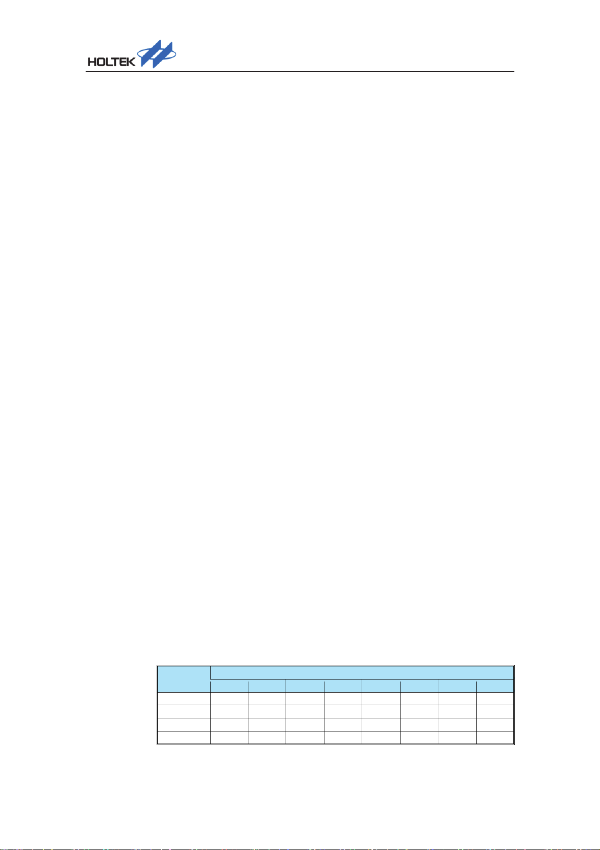
The clock frequency block diagram is shown as below.
f
H
fH/2
/4
f
H
/8
f
H
f
H
f
H
f
H
/16
/32
/64
CKS2~CKS 0
f
SYS
f
SUB
resistor together with the C1
P
HIRCEN
HXTEN
High Speed
Oscillat or
HIRC
HXT
Low Speed
Oscillat or
LXT
f
LXT
FHS
IDLE2
SLEEP
f
H
Prescaler
f
SUB
LXT Oscillator
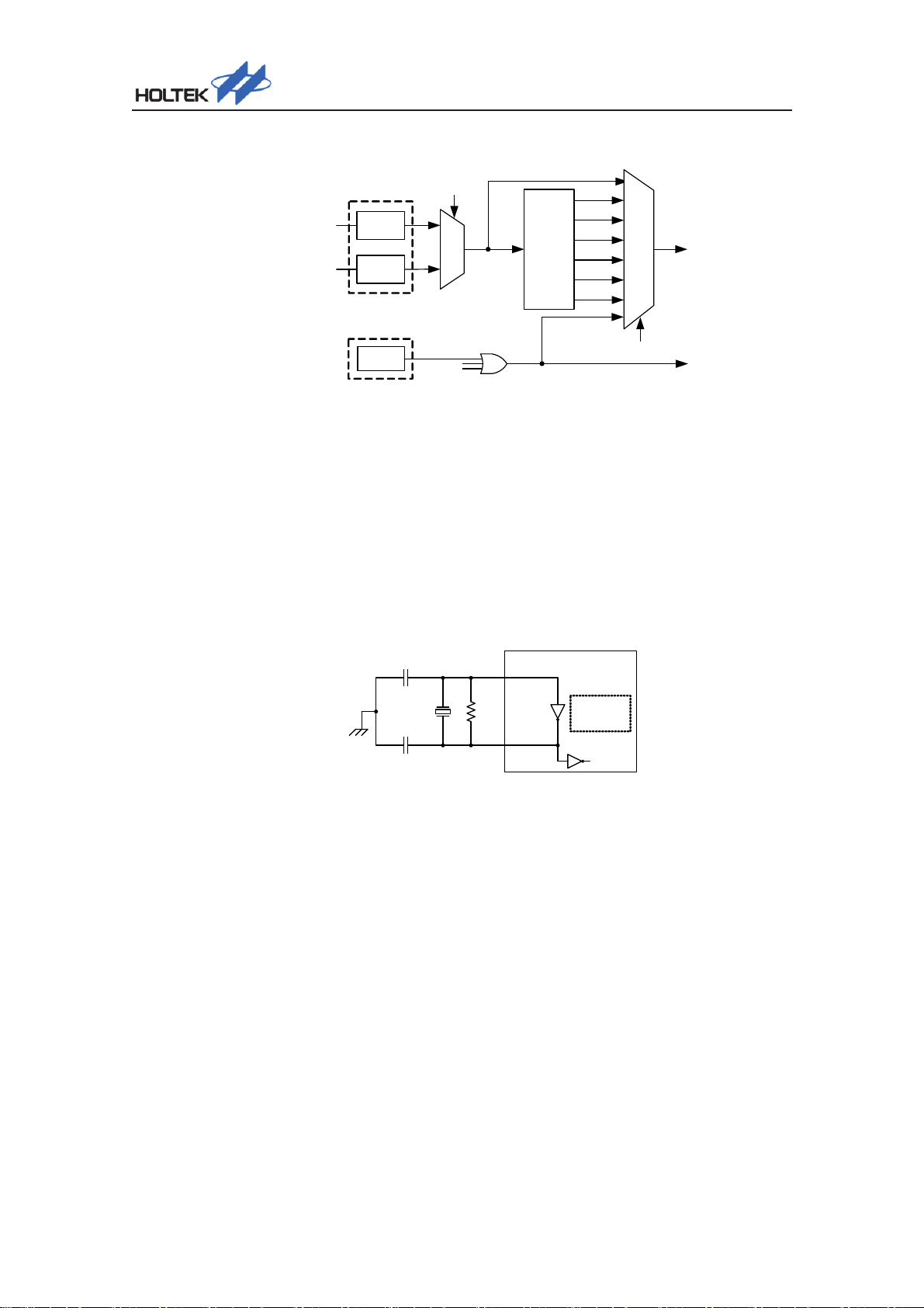
The LXT oscillation circuit consists of an external 32768Hz crystal and resistor as well as
capacitor components. The crystal is connected between pins XT1 and XT2. The
frequency accuracy adjustment is implemented by the R
and C2 capacitors. Users should refer to the oscillator specification for the resistance and
capacitance configurations. After power on the LXTEN bit will be in a high state which
enable the LXT oscillator. By examining if the LXTF bit has been set high, it can be
determined if the LXT oscillator is powered up and ready for use. The LXT oscillator
circuit is shown as below.
C1
32. 768kHz
C2
Note : 1. RP, C1 and C 2 ar e required .
2. Al though not shown pi ns have a paras iti c capaci tance of ar ound 7pF .
XT1
R
P
XT2
Internal
Oscillator
Circuit
Internal RC
Oscillator
To internal
circuits
External LXT Oscillator
Time Base Control Register
The HT67F86A provides a Real Time Clock function. A time counting function can be
implemented by configuring the Time Base 0 or Time Base 1 interrupt control bits, TB0E
or TB1E, together with the data memory. The time base function clock source, f
from the f
registers to choose a value within the range of f
. The Time Base frequency division ratio is selected by configuring the
LXT
PSC
/28 ~ f
/215. Refer to the datasheet for
PSC
the related registers and the TB0E and TB1E interrupt addresses.
PSC,
comes
AN0448E V1.00 2/7 January 16, 2017
Page 3
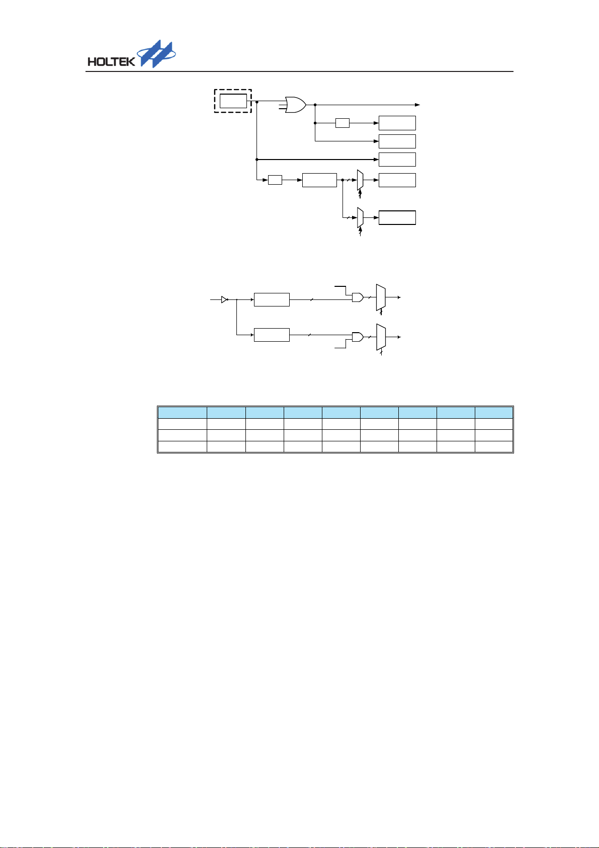
HT67F86A Internal RTC Application Guidelines
f
LXT
LXT
Low Speed
Oscillat or
IDLE2
SLEEP
f
SUB
f
/4
LXT
1/4 Time Base 0
Prescaler
1/8
f
SUB
f
LXT
TB0 [2:0]
f
LCD
Time Base 1
LCD
LVR
WDT
f
SUB
TB1[2:0]
Device Clock Configuration
TB0ON
f
f
/4
LXT
PSC
Prescaler 0
Prescaler 1
f
PSC
f
PSC
/28~ f
/28~ f
PSC
PSC
TB1ON
15
/2
15
/2
Time Base Interrupt
TB0C Register
Bit 7 6 5 4 3 2 1 0
Name TB0ON — — — — TB02 TB01 TB00
R/W R/W — — — — R/W R/W R/W
POR 0 — — — — 0 0 0
Bit 7 TB0ON: Time Base 0 Enable Control
0: Disable
1: Enable
Bit 6~3 Unimplemented, read as “0”
Bit 2~0 TB02~TB00: Time Base 0 time-out period selection
8
000: 2
/f
PSC
9
001: 2
/f
PSC
10
010: 2
011: 2
100: 2
101: 2
110: 2
111: 2
The f
/f
PSC
11
/f
PSC
12
/f
PSC
13
/f
PSC
14
/f
PSC
15
/f
PSC
is derived from the internal clock source f
PSC
M
U
X
TB0 [2:0]
M
U
X
TB1 [2:0]
Time Base 0 Interrupt
Time Base 1 Interrupt
/4.
LXT
AN0448E V1.00 3/7 January 16, 2017
Page 4

HT67F86A Internal RTC Application Guidelines
TB1C Register
Bit 7 6 5 4 3 2 1 0
Name TB1ON — — — — TB12 TB11 TB10
R/W R/W — — — — R/W R/W R/W
POR 0 — — — — 0 0 0
Bit 7 TB1ON: Time Base 1 Enable Control
0: Disable
1: Enable
Bit 6~3 Unimplemented, read as “0”
Bit 2~0 TB12~TB10: Time Base 1 time-out period selection
The f
8
/f
000: 2
001: 29/f
010: 2
011: 2
100: 212/f
101: 2
110: 2
111: 215/f
PSC
PSC
PSC
10
/f
PSC
11
/f
PSC
PSC
13
/f
PSC
14
/f
PSC
PSC
is derived from the internal clock source f
LXT
/4.
Internal RTC Characteristics
Operating Voltage
The internal RTC operating voltage depends on the LXT oscillator which has a voltage
range of 2.2V~5.5V. Such applications are suitable for battery powered products which
require 2~3 batteries. Refer to the “Low Speed Crystal Oscillator Characteristics – LXT”
section in the datasheet or the following table for the related voltage characteristics.
Symbol Parameter
f
Oscillator Frequency
LXT
Duty
Cycle
t
START
R
NEG
Duty Cycle — — 45 50 55 %
LXT Start-up Time — — — — 500 ms
Negative Resistance
Note
Note: C1, C2 and RP are external components. C1=C2=15pF, RP=10MΩ, CL=7pF,
ESR=30kΩ.
Test Condition
VDD Condition
2.2V~
5.5V
2.2V — 3×ESR — — Ω
=32.768kHz —
f
SYS=fLXT
Ta=25°C
Min. Typ. Max. Unit
32.76
8
— kHz
AN0448E V1.00 4/7 January 16, 2017
Page 5

HT67F86A Internal RTC Application Guidelines
Negative Impedance
The LXT oscillator provides a negative impedance reference and for safety provides a value
which is at least 3 times that of the ESR to avoid oscillation problems in mass production.
Special attention should be made with regard to this when using the 32768Hz crystal.
Oscillation Frequency
The LXT oscillator oscillation frequency is mainly determined by the 32768Hz crystal
capacitance C
capacitance values together with the PCB parasitic capacitance is equal to the crystal
capacitance C
adjust the oscillation frequency to determine the appropriate C1 and C2 capacitance. It
should be noted that the oscillation frequency will be lower if the chosen C1 and C2
capacitors are greater than C
oscillation frequency curve used by the MCU should be taken into account for temperature
deviation. Note that checking the oscillation frequency by directly using an oscilloscope
probe is inadvisable. The best way to check the frequency is using the I/O pins.
For example, if the external capacitors C1 and C2 series equivalent
L.
, then an accurate frequency of 32768Hz can be achieved. The user can
L
and vice versa. The crystal related characteristics and the
L
Standby Power Consumption
When the LXT is in an oscillating state together and the Time Base clock circuit turned on to
reduce power, it can provides a low MCU standby power consumption of lower than 1µA at
an operating voltage of 3V, thus achieve longer service life for battery-powered products.
This means that the HT67F86A forms an excellent choice for power sensitive applications.
As well as considerations regarding the frequency characteristics, the user should also pay
attention to the standby power consumption when selecting the crystal CL and external C1
and C2 capacitors. The common CL capacitance is 12.5pF. When measuring the standby
current not that scope probes should not be placed on any MCU pins.
Symbol
I
STB
Standby Mode
SLEEP Mode
IDLE0 Mode
Test Condition
VDD Condition
3V
WDT off, Time Base on
5V — 0.8 1.5
3V
WDT on
5V — 0.9 3.0
3V
f
on
SUB
5V — 1.5 5.0
Min. Typ. Max. Unit
— 0.6 1.0
— 0.7 1.5
— 1.0 3.0
µA
µA
µA
PCB Planning Considerations
During circuit design, designers should select an appropriate feedback resistor RP, with a
resistance range of between 5MΩ and 10MΩ, and capacitors C1 and C2 for a matched
oscillation frequency after the frequency test. Any high frequency circuits located close to
the LXT circuit, will influence the oscillator characteristics, therefore special care must be
taken in such cases. The LXT oscillator circuit should be located as close to the XT1/XT2
pins as possible while the interconnecting lines between the C1/C2 capacitors and VSS
should be as short as possible. The reference circuit is shown below.
AN0448E V1.00 5/7 January 16, 2017
Page 6

HT67F86A Internal RTC Application Guidelines
Application Range
Token Card Reader
Online banking, transactions using mobile devices, such as cellphones and tablets, can
be carried out using a Bluetooth connected smart card reader. As these devices are
normally battery powered, the HT67F86A is an excellent choice for these applications
due to its low power consumption and 1024 pixel LCD driver.
Consumer Products
The HT67F86A internal Real Time Clock function can be applied for use in a wide range
of battery powered consumer products such as electronic alarm clocks etc.
Conclusion
This application note summarises the internal RTC usage considerations providing
reference information for designers.
Reference Files
Reference file: HT67F86A Datasheet.
For more information, refer to the Holtek official website http://www.holtek.com/en.
AN0448E V1.00 6/7 January 16, 2017
Page 7

HT67F86A Internal RTC Application Guidelines
Version and Modification Information
Date Author Issue
Disclaimer
All information, trademarks, logos, graphics, videos, audio clips, links and other items
appearing on this website ('Information') are for reference only and is subject to change at
any time without prior notice and at the discretion of Holtek Semiconductor Inc. (herein
after 'Holtek', 'the company', 'us', 'we' or 'our'). Whilst Holtek endeavors to ensure the
accuracy of the Information on this website, no express or implied warranty is given by
Holtek to the accuracy of the Information. Holtek shall bear no responsibility for any
incorrectness or leakage.
Holtek shall not be liable for any damages (including but not limited to computer virus,
system problems or data loss) whatsoever arising in using or in connection with the use of
this website by any party. There may be links in this area, which allow you to visit the
websites of other companies. These websites are not controlled by Holtek. Holtek will
bear no responsibility and no guarantee to whatsoever Information displayed at such sites.
Hyperlinks to other websites are at your own risk.
2016.12.20
黃啟德
First Version
Limitation of Liability
In no event shall Holtek Limited be liable to any other party for any loss or damage
whatsoever or howsoever caused directly or indirectly in connection with your access to
or use of this website, the content thereon or any goods, materials or services.
Governing Law
The Disclaimer contained in the website shall be governed by and interpreted in
accordance with the laws of the Republic of China. Users will submit to the non-exclusive
jurisdiction of the Republic of China courts.
Update of Disclaimer
Holtek reserves the right to update the Disclaimer at any time with or without prior notice,
all changes are effective immediately upon posting to the website.
AN0448E V1.00 7/7 January 16, 2017
 Loading...