

Page 1

Advanced A/D Flash MCU with LCD & EEPROM
HT67F2350/HT67F2360
HT67F2370/HT67F2390
Revision: V1.60 Date: May 16, 2019
Page 2

HT67F2350/HT67F2360
HT67F2370/HT67F2390
Advanced A/D Flash MCU with LCD & EEPROM
Table of Contents
Features ............................................................................................................ 7
CPU Features ......................................................................................................................... 7
Peripheral Features ................................................................................................................. 7
General Description ......................................................................................... 8
Selection Table ................................................................................................. 8
Block Diagram .................................................................................................. 9
Pin Assignment ................................................................................................ 9
Pin Descriptions ............................................................................................ 14
Absolute Maximum Ratings .......................................................................... 40
D.C. Characteristics ....................................................................................... 40
Operating Voltage Characteristics ......................................................................................... 40
Standby Current Characteristics ........................................................................................... 41
Operating Current Characteristics ......................................................................................... 42
A.C. Characteristics ....................................................................................... 43
High Speed Internal Oscillator – HIRC – Frequency Accuracy ............................................. 43
Low Speed Internal Oscillator Characteristics – LIRC .......................................................... 43
Low Speed Crystal Oscillator Characteristics – LXT ............................................................. 43
Operating Frequency Characteristic Curves ......................................................................... 44
System Start Up Time Characteristics .................................................................................. 44
Input/Output Characteristics ........................................................................ 45
Memory Characteristics ................................................................................ 46
LVD/LVR Electrical Characteristics .............................................................. 46
A/D Converter Characteristics ...................................................................... 47
Comparator Electrical Characteristics ........................................................ 48
LCD Driver Electrical Characteristics .......................................................... 49
I2C Characteristics ......................................................................................... 49
Power-on Reset Characteristics ................................................................... 50
System Architecture ...................................................................................... 51
Clocking and Pipelining ......................................................................................................... 51
Program Counter ................................................................................................................... 52
Stack ..................................................................................................................................... 53
Arithmetic and Logic Unit – ALU ........................................................................................... 53
Flash Program Memory ................................................................................. 54
Structure ................................................................................................................................ 54
Special Vectors ..................................................................................................................... 54
Look-up Table ........................................................................................................................ 54
Table Program Example ........................................................................................................ 56
In Circuit Programming – ICP ............................................................................................... 57
On-Chip Debug Support – OCDS ......................................................................................... 58
Rev. 1.60 2 May 16, 2019 Rev. 1.60 3 May 16, 2019
Page 3

HT67F2350/HT67F2360
HT67F2370/HT67F2390
Advanced A/D Flash MCU with LCD & EEPROM
In Application Programming – IAP ........................................................................................ 58
Data Memory .................................................................................................. 67
Structure ................................................................................................................................ 67
Data Memory Addressing ...................................................................................................... 68
General Purpose Data Memory ............................................................................................ 68
Special Purpose Data Memory ............................................................................................. 68
Special Function Register Description ........................................................ 72
Indirect Addressing Registers – IAR0, IAR1, IAR2 ............................................................... 72
Memory Pointers – MP0, MP1H/MP1L, MP2H/MP2L ........................................................... 72
Program Memory Bank Pointer – PBP .................................................................................. 74
Accumulator – ACC ............................................................................................................... 75
Program Counter Low Register – PCL .................................................................................. 75
Look-up Table Registers – TBLP, TBHP, TBLH ..................................................................... 75
Status Register – STATUS .................................................................................................... 75
EEPROM Data Memory .................................................................................. 77
EEPROM Data Memory Structure ........................................................................................ 77
EEPROM Registers .............................................................................................................. 77
Reading Data from the EEPROM ......................................................................................... 79
Writing Data to the EEPROM ................................................................................................ 80
Write Protection ..................................................................................................................... 80
EEPROM Interrupt ................................................................................................................ 80
Programming Considerations ................................................................................................ 81
Oscillators ...................................................................................................... 82
Oscillator Overview ............................................................................................................... 82
System Clock Congurations ................................................................................................ 82
External Crystal/Ceramic Oscillator – HXT ........................................................................... 83
Internal High Speed RC Oscillator – HIRC ........................................................................... 84
External 32.768 kHz Crystal Oscillator – LXT ....................................................................... 84
Internal 32kHz Oscillator – LIRC ........................................................................................... 85
Operating Modes and System Clocks ......................................................... 85
System Clocks ...................................................................................................................... 85
System Operation Modes ...................................................................................................... 87
Control Registers .................................................................................................................. 88
Operating Mode Switching .................................................................................................... 91
Standby Current Considerations ........................................................................................... 95
Wake-up ................................................................................................................................ 95
Watchdog Timer ............................................................................................. 96
Watchdog Timer Clock Source .............................................................................................. 96
Watchdog Timer Control Register ......................................................................................... 96
Watchdog Timer Operation ................................................................................................... 97
Reset and Initialisation .................................................................................. 98
Reset Functions .................................................................................................................... 98
Reset Initial Conditions ....................................................................................................... 102
Page 4

HT67F2350/HT67F2360
HT67F2370/HT67F2390
Advanced A/D Flash MCU with LCD & EEPROM
Input/Output Ports ........................................................................................110
Pull-high Resistors ...............................................................................................................112
Port A Wake-up ....................................................................................................................112
I/O Port Control Registers ....................................................................................................113
I/O Port Source Current Control ...........................................................................................113
Pin-shared Functions ...........................................................................................................117
I/O Pin Structures ................................................................................................................ 130
READ PORT Function......................................................................................................... 131
Programming Considerations .............................................................................................. 132
Timer Modules – TM .................................................................................... 133
Introduction ......................................................................................................................... 133
TM Operation ...................................................................................................................... 133
TM Clock Source ................................................................................................................. 133
TM Interrupts ....................................................................................................................... 134
TM External Pins ................................................................................................................. 134
TM Input/Output Pin Selection ............................................................................................ 135
Programming Considerations .............................................................................................. 136
Standard Type TM – STM ............................................................................ 137
Standard TM Operation ....................................................................................................... 137
Standard Type TM Register Description ............................................................................. 138
Standard Type TM Operation Modes .................................................................................. 142
Periodic Type TM – PTM .............................................................................. 152
Periodic TM Operation ........................................................................................................ 153
Periodic Type TM Register Description ............................................................................... 153
Periodic Type TM Operation Modes .................................................................................... 158
Analog to Digital Converter ........................................................................ 167
A/D Overview ...................................................................................................................... 167
Registers Descriptions ........................................................................................................ 168
A/D Converter Reference Voltage ....................................................................................... 172
A/D Converter Input Signals ................................................................................................ 173
A/D Operation ..................................................................................................................... 174
Conversion Rate and Timing Diagram ................................................................................ 175
Summary of A/D Conversion Steps ..................................................................................... 176
Programming Considerations .............................................................................................. 177
A/D Transfer Function ......................................................................................................... 177
A/D Programming Examples ............................................................................................... 178
Serial Interface Module – SIM ..................................................................... 180
SPI Interface ....................................................................................................................... 180
I2C Interface ........................................................................................................................ 186
Serial Interface – SPIA ................................................................................. 196
SPIA Interface Operation .................................................................................................... 196
SPIA Registers .................................................................................................................... 197
SPIA Communication .......................................................................................................... 200
SPIA Bus Enable/Disable .................................................................................................... 202
Rev. 1.60 4 May 16, 2019 Rev. 1.60 5 May 16, 2019
Page 5

HT67F2350/HT67F2360
HT67F2370/HT67F2390
Advanced A/D Flash MCU with LCD & EEPROM
SPIA Operation ................................................................................................................... 202
Error Detection .................................................................................................................... 203
UART Interface ............................................................................................. 204
UART External Pin .............................................................................................................. 205
UART Data Transfer Scheme.............................................................................................. 205
UART Status and Control Registers.................................................................................... 205
Baud Rate Generator .......................................................................................................... 210
UART Setup and Control......................................................................................................211
UART Transmitter................................................................................................................ 212
UART Receiver ................................................................................................................... 214
Managing Receiver Errors .................................................................................................. 215
UART Interrupt Structure..................................................................................................... 216
UART Power Down and Wake-up ....................................................................................... 218
Comparators ................................................................................................ 219
Comparator Operation ........................................................................................................ 219
Comparator Registers ......................................................................................................... 219
Input Offset Calibration ....................................................................................................... 221
Comparator Interrupt ........................................................................................................... 221
Programming Considerations .............................................................................................. 221
LCD Driver .................................................................................................... 222
LCD Memory ....................................................................................................................... 224
LCD Clock Source ............................................................................................................... 225
LCD Register ....................................................................................................................... 225
LCD Voltage Source and Biasing ........................................................................................ 227
LCD Reset Function ............................................................................................................ 228
LCD Driver Output ............................................................................................................... 229
Programming Considerations .............................................................................................. 238
16-bit Multiplication Division Unit – MDU .................................................. 239
MDU Registers .................................................................................................................... 239
MDU Operation ................................................................................................................... 240
Cyclic Redundancy Check – CRC .............................................................. 242
CRC Registers .................................................................................................................... 242
CRC Operation .................................................................................................................... 243
Low Voltage Detector – LVD ....................................................................... 245
LVD Register ....................................................................................................................... 245
LVD Operation ..................................................................................................................... 246
Interrupts ...................................................................................................... 247
Interrupt Registers ............................................................................................................... 247
Interrupt Operation .............................................................................................................. 257
External Interrupt ................................................................................................................. 259
Multi-function Interrupt ........................................................................................................ 259
A/D Converter Interrupt ....................................................................................................... 259
TM Interrupt ......................................................................................................................... 260
LVD Interrupt ....................................................................................................................... 260
Page 6

HT67F2350/HT67F2360
HT67F2370/HT67F2390
Advanced A/D Flash MCU with LCD & EEPROM
EEPROM Interrupt .............................................................................................................. 260
Serial Interface Module Interrupt ......................................................................................... 260
SPIA Interface Interrupt ....................................................................................................... 261
UART Transfer Interrupt ...................................................................................................... 261
Comparator Interrupt ........................................................................................................... 261
Time Base Interrupt ............................................................................................................. 262
Interrupt Wake-up Function ................................................................................................. 264
Programming Considerations .............................................................................................. 264
Application Circuits ..................................................................................... 265
Instruction Set .............................................................................................. 266
Introduction ......................................................................................................................... 266
Instruction Timing ................................................................................................................ 266
Moving and Transferring Data ............................................................................................. 266
Arithmetic Operations .......................................................................................................... 266
Logical and Rotate Operation ............................................................................................. 267
Branches and Control Transfer ........................................................................................... 267
Bit Operations ..................................................................................................................... 267
Table Read Operations ....................................................................................................... 267
Other Operations ................................................................................................................. 267
Instruction Set Summary ............................................................................ 268
Table Conventions ............................................................................................................... 268
Extended Instruction Set ..................................................................................................... 270
Instruction Denition ................................................................................... 272
Extended Instruction Denition ........................................................................................... 281
Package Information ................................................................................... 288
48-pin LQFP (7mm×7mm) Outline Dimensions .................................................................. 289
64-pin LQFP (7mm×7mm) Outline Dimensions .................................................................. 290
80-pin LQFP (10mm×10mm) Outline Dimensions .............................................................. 291
Rev. 1.60 6 May 16, 2019 Rev. 1.60 7 May 16, 2019
Page 7

HT67F2350/HT67F2360
HT67F2370/HT67F2390
Advanced A/D Flash MCU with LCD & EEPROM
Features
CPU Features
• Operating Voltage:
♦
f
=8MHz: 2.2V~5.5V
SYS
♦
f
=12MHz: 2.7V~5.5V
SYS
♦
f
=16MHz: 3.3V~5.5V
SYS
• Up to 0.25μs instruction cycle with 16MHz system clock at VDD=5V
• Power down and wake-up functions to reduce power consumption
• Oscillator Types:
♦
External High Speed Crystal – HXT
♦
Internal High Speed RC – HIRC
♦
External 32.768kHz Crystal – LXT
♦
Internal 32kHz RC – LIRC
• Fully integrated internal 8/12/16 MHz oscillator requires no external components
• Multi-mode operation: FAST, SLOW, IDLE and SLEEP
• All instructions executed in one to three instruction cycles
• Table read instructions
• 115 powerful instructions
• 16-level subroutine nesting
• Bit manipulation instruction
Peripheral Features
• Program Memory: Up to 64K×16
• Data Memory: Up to 4096×8
• True EEPROM Memory: Up to 1024×8
• Watchdog Timer function
• Up to 71 bidirectional I/O lines
• Programmable I/O source current
• LCD Driver function with 1/3 or 1/4 bias
• Four external interrupt lines shared with I/O pins
• Multiple Timer Modules for time measure, input capture, compare match output, PWM output
function or single pulse output function
• Serial Interface Module – includes SPI and I2C
• Additional Serial Peripheral Interface – SPIA
• Up to three Fully-duplex Universal Asynchronous Receiver and Transmitter Interfaces – UARTs
• Dual Time-Base functions for generation of xed time interrupt signals
• Dual comparator functions
• Up to 16 external channel 12-bit resolution A/D converter
• Integrated Multiplier/Divider Unit – MDU
• Integrated 16-bit Cyclic Redundancy Check function – CRC
• Low voltage reset function
• Low voltage detect function
• European standard IEC 60730 and U.S. UL 60730 certied
• Wide range of package types
Page 8
General Description
This series of devices are LCD type Flash Memory 8-bit high performance RISC architecture
microcontrollers which are designed for a wide range of applications. Offering users the convenience
of Flash Memory multi-programming features, these devices also include a wide range of functions
and features. Other memory includes an area of RAM Data Memory as well as an area of true
EEPROM memory for storage of non-volatile data such as serial number, calibration data, etc.
Analog features include a multi-channel 12-bit A/D converter and dual comparator functions. Multiple
and extremely flexible Timer Modules provide timing, pulse generation and PWM generation
functions. Communication with the outside world is catered for by including fully integrated SPI,
UART or I2C interface functions, three popular interfaces which provide designers with a means
of easy comminucation with external peripheral hardware. Protective features such as an internal
Watchdog Timer, Low Voltage Reset and Low Voltage Detector coupled with excellent noise immunity
and ESD protection ensure that reliable operation is maintained in hostile electrical environments.
A full choice of HXT, LXT, HIRC and LIRC oscillator functions are provided including a fully
integrated system oscillator which requires no external components for its implementation. The ability
to operate and switch dynamically between a range of operating modes using different clock sources
gives users the ability to optimise microcontroller operation and minimise power consumption.
The inclusion of exible I/O programming features, Time-Base functions along with many other
features ensure that the devices will nd excellent use in applications such as electronic metering,
environmental monitoring, handheld instruments, household appliances, electronically controlled
tools, motor driving in addition to many others.
HT67F2350/HT67F2360
HT67F2370/HT67F2390
Advanced A/D Flash MCU with LCD & EEPROM
Selection Table
Most features are common to all devices. The main features distinguishing them are Memory
capacity, I/O count, A/D converter channel number, LCD driver pin count and UART interface
number. The following table summarises the main features of each device.
Part No.
HT67F2350 8k × 16 768 × 8 256 × 8 57 4 12-bit × 12
HT67F2360 16k × 16 1536 × 8 256 × 8 71 4 12-bit × 16
HT67F2370 32k × 16 3072 × 8 512 × 8 71 4 12-bit × 16
HT67F2390 64k × 16 4096 × 8 1024 × 8 71 4 12-bit × 16
Part No.
HT67F2350 2 2 16 √ √ 2 √ √ 48/64LQFP
HT67F2360 2 2 16 √ √ 2 √ √ 64/80LQFP
HT67F2370 2 2 16 √ √ 3 √ √ 64/80LQFP
HT67F2390 2 2 16 √ √ 3 √ √ 64/80LQFP
Program
Memory
Time
Base
Note: As devices exist in more than one package format, the table reects the situation for the package with the
most pins.
Data
Memory
Comparators Stacks SIM SPIA UART MDU CRC Package
Data
EEPROM
I/O
External
Interrupt
A/D
LCD Driver
(SEGm × COMn)
46 × 4
44 × 6
42 × 8
56 × 4
54 × 6
52 × 8
56 × 4
54 × 6
52 × 8
56 × 4
54 × 6
52 × 8
Timer Module
10-bit PTM × 6
16-bit PTM × 2
16-bit STM × 3
10-bit PTM × 6
16-bit PTM × 2
16-bit STM × 3
10-bit PTM × 6
16-bit PTM × 2
16-bit STM × 3
10-bit PTM × 6
16-bit PTM × 2
16-bit STM × 3
Rev. 1.60 8 May 16, 2019 Rev. 1.60 9 May 16, 2019
Page 9
HT67F2350/HT67F2360
HT67F2370/HT67F2390
Advanced A/D Flash MCU with LCD & EEPROM
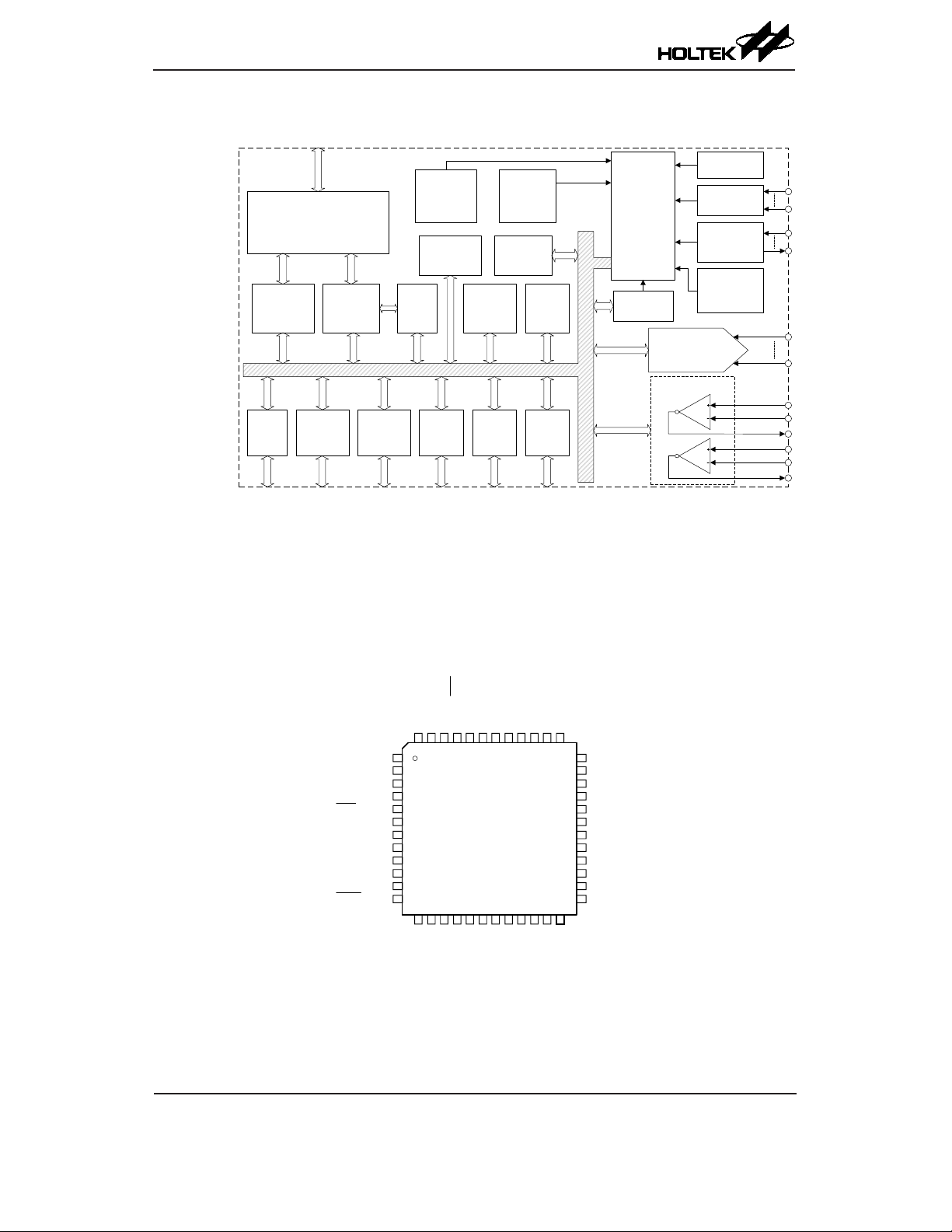
Block Diagram
Memory
Low
Voltage
Reset
CRC
Time
Base
Flash/EEPROM
Programming Circuitry
EEPROM
Data
Memory
Flash
Program
Memory
IAP
Low
Voltage
Detect
MDU
RAM Data
8-bit
RISC
MCU
Core
Watchdog
Timer
Interrupt
Controller
External
HXT/LXT
Oscillators
HIRC/LIRC
Oscillators
12-bit A/D
Converter
Comparators
Reset
Circuit
Internal
I/Os
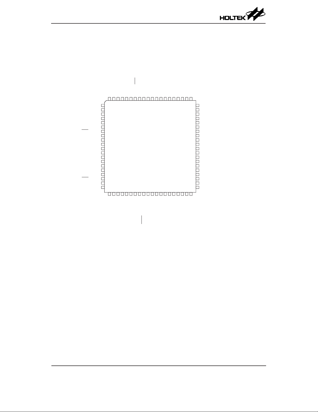
Pin Assignment
PB6/STP1I/STP1/OSC1/SEG35
PB7/STCK1/OSC2/SEG34
PA0/SEG30/ICPDA/OCDSDA
PA2/SEG29/ICPCK/OCDSCK
PA4/INT2/SDI/SDA/SEG24
PA5/INT3/SCK/SCL/SEG23
PB2/PTP3I/PTCK2/PTP3/SEG16
Timer
Modules
PA1/INT0/SCS/SEG26
PA3/INT1/SDO/SEG25
PA6/INT0/RX0/SEG22
PA7/INT1/TX0/SEG21
PE0/STCK0/SCSA/SEG7
SIM
(SPI/I
UARTs
2
C)
VDD
VSS
1
2
3
4
5
HT67F2350/HT67V2350
6
7
8
9
10
11
12
13 14 15 16 17 18 19 20 21 22 23 24
PE1/STP0I/STP0/SDOA/SEG6
PE2/PTCK1/SDIA/SEG5
PF7/STP2I/STP2/TX1/C0+
PB5/RES/SEG36
45
464748 3738394041424344
48 LQFP-A
PE3/PTP1I/PTP1/SCKA/SEG4
PE4
SPIA
PD3/PTCK2/PTP7I/PTP7/AN11/SEG43
PF6/STCK2/RX1/C0−/SEG37
PD2/PTP2I/PTP2/TX1/AN10
PJ3/COM7/SEG3
PJ2/COM6/SEG2
PJ1/COM5/SEG1
PJ0/COM4/SEG0
AVSS
PF5/PTP0I/PTP0/XT1
PG7/COM3
LCD
Driver
PF4/PTCK0/XT2
AVDD
PG6/COM2
PG5/COM1
PD1/STCK1/RX1/AN9/SEG44
PD0/INT2/STP1I/STP1/AN8/SEG45
36
35
PC7/INT3/STCK0/PTP6I/PTP6/AN7/SEG46
PC5/PTCK1/PTP5I/PTP5/AN5/SEG48
34
PC3/PTCK0/PTP4I/PTP4/AN3/SEG50
33
PC1/C0X/VREF/AN1
32
31
PC0/VREFI/AN0/SEG52
PLCD
30
VMAX
29
28
V1
27
PE7/V2/SEG53
PE6/C1/SEG54
26
25
PE5/C2/SEG55
PG4/COM0
Page 10
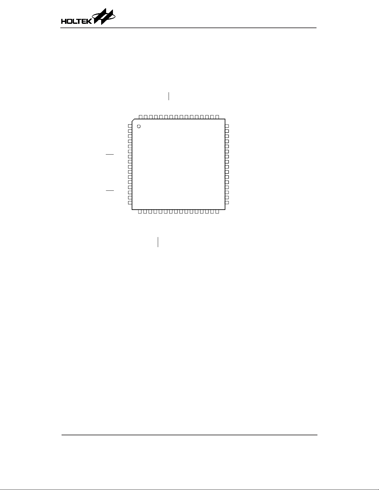
HT67F2350/HT67F2360
HT67F2370/HT67F2390
Advanced A/D Flash MCU with LCD & EEPROM
PD3/PTCK2/PTP7I/PTP7/AN11/SEG43
PB6/STP1I/STP1/OSC1/SEG35
PD6/STP2I/STP2/C1X/SEG33
PB7/STCK1/OSC2/SEG34
VSS
VDD
PF6/STCK2/RX1/C0−/SEG37
PD5/PTCK3/TX0/C1+/SEG38
PD2/PTP2I/PTP2/TX1/A N10
PD4/PTP3I/PTP3/RX0/C1−
PF7/STP2I/STP2/TX1/C0+
PF5/PTP0I/PTP0/XT1
PB5/RES/SEG36
PF4/PTCK0/XT2
AVSS
AVDD
PB0/STCK2/C0X/SEG32
PB1/PTCK3/SEG31
PA0/SEG30/ICPDA/OCDSDA
PA2/SEG29/ICPCK/OCDSCK
PB4/C1X/SEG28
PB3/PTP2I/PTP2/SEG27
PA1/INT0/SCS/SEG26
PA3/INT1/SDO/SEG25
PA4/INT2/SDI/SDA/SEG24
PA5/INT3/SCK/SCL/SEG23
PA6/INT0/RX0/SEG22
PA7/INT1/TX0/SEG21
PB2/PTP3I/PTCK2/PTP3/SEG16
PF0/SCS/SEG15
PF1/SDO/SEG14
PF2/SDI/SDA/SEG13
1
2
3
4
5
6
7
8
9
10
11
12
13
14
15
16
17 18 19
6061626364
HT67F2350/HT67V2350
HT67F2360/HT67V2360
20 21 22 23 24 25 26 27 28
PF3/SCK/SCL/SEG12
PJ7/PTCK4/SEG11
PJ6/PTCK5/SEG10
PE1/STP0I/STP0/SDOA/SEG6
PE0/STCK0/SCSA/SEG7
64 LQFP-A
PE2/PTCK1/SDIA/S EG5
PE3/PTP1I/PTP1/SCKA/SEG4
PE4
PJ3/COM7/SEG3
PJ2/COM6/SEG2
PJ1/COM5/SEG1
5253545556575859
29 30 31 32
PJ0/COM4/SEG0
PG7/COM3
495051
PD1/STCK1/RX1/AN9/SEG4 4
48
PD0/INT2/STP1I/STP1/AN8/SEG45
47
PC7/INT3/STCK0/PTP6I/PTP6/AN7/SEG46
46
PC6/STP0I/STP0/AN6/SEG47
45
PC5/PTCK1/PTP5I/PTP5/AN5/SEG48
44
PC4/PTP1I/PTP1/AN4/SEG49
43
PC3/PTCK0/PTP4I/PTP4/AN3/SEG50
42
PC2/PTP0I/PTP0/AN2/SEG51
41
PC1/C0X/VREF/AN1
40
PC0/VREFI/AN0/SEG52
39
PLCD
38
VMAX
37
V1
36
PE7/V2/SEG53
35
PE6/C1/SEG54
34
PE5/C2/SEG55
33
PG6/COM2
PG5/COM1
PG4/COM0
Rev. 1.60 10 May 16, 2019 Rev. 1.60 11 May 16, 2019
Page 11
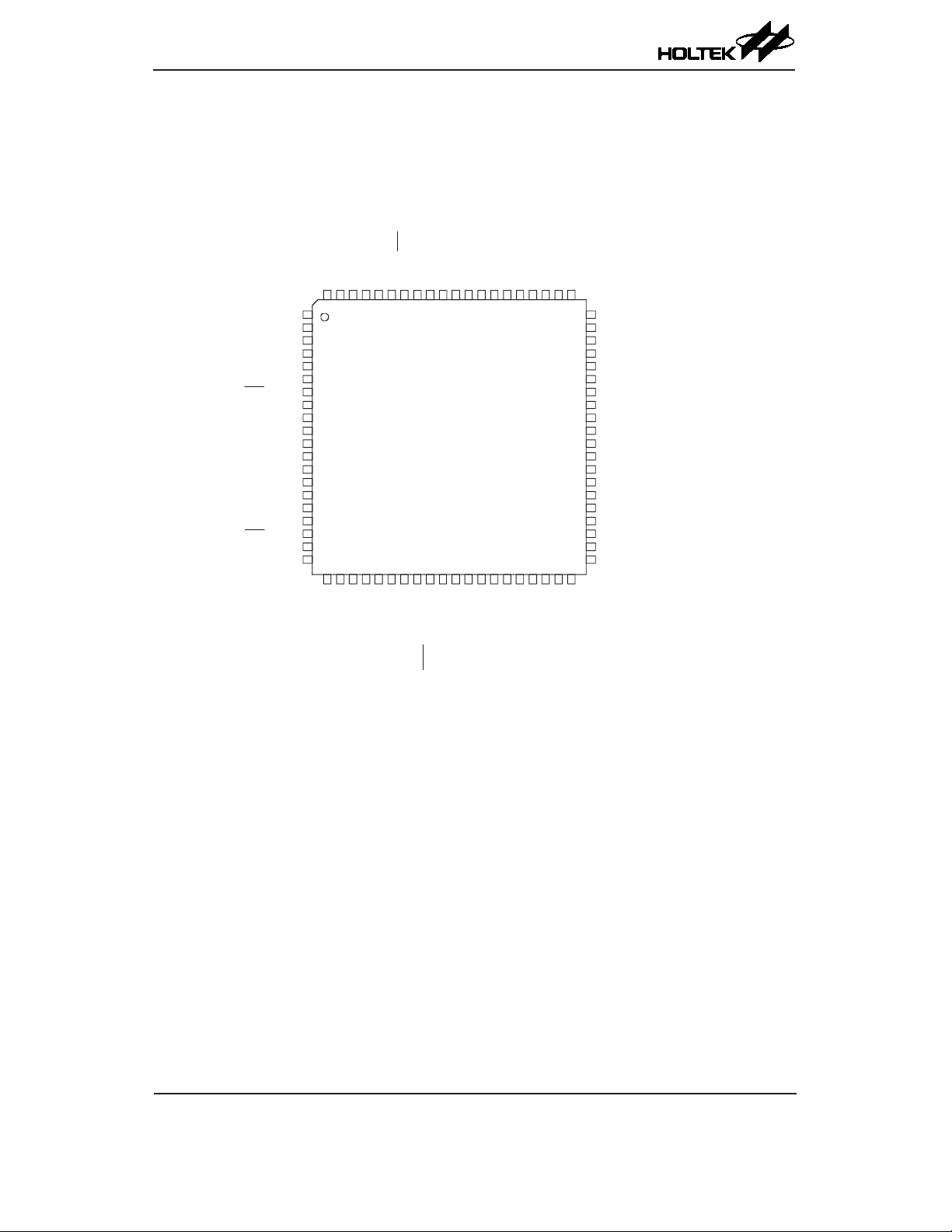
HT67F2350/HT67F2360
HT67F2370/HT67F2390
Advanced A/D Flash MCU with LCD & EEPROM
PD3/PTCK2/PTP7I/PTP7/AN11/SEG43
PB6/STP1I/STP1/OSC1/SEG35
PB0/STCK2/C0X/SEG32
PB1/PTCK3/SEG31
PA0/SEG30/ICPDA/OCDSDA
PA2/SEG29/ICPCK/OCDSCK
PB4/C1X/SEG28
PB3/PTP2I/PTP2/SEG27
PA1/INT0/SCS/SEG26
PA3/INT1/SDO/SEG25
PA4/INT2/SDI/SDA/SEG24
PA5/INT3/SCK/SCL/SEG23
PA6/INT0/RX0/SEG22
PA7/INT1/TX0/SEG21
PH0/PTP4I/PTP4/SEG20
PH1/PTP5I/PTP5/SEG19
PH6/PTP6I/PTP6/SEG18
PH7/PTP7I/PTP7/SEG17
PB2/PTP3I/PTCK2/PTP3/SEG16
PF0/SCS/SEG15
PF1/SDO/SEG14
PF2/SDI/SDA/SEG13
PD6/STP2I/STP2/C1X/SEG33
PB7/STCK1/OSC2/SEG34
VSS
80
79 78 77 76 75 74 73 72 71 70 69 68 67 66 65 64 63 62 61
1
2
3
4
5
6
7
8
9
10
11
12
13
14
15
16
17
18
19
20
21
22 23 24 25 26 27 28 29 30 31 32 33 34 35 36 37 38 39 40
PF3/SCK/SCL/SEG12
PJ7/PTCK4/SEG11
PJ6/PTCK5/SEG10
PJ5/PTCK6/SEG9
PF6/STCK2/RX1/C0−/SEG37
PD5/PTCK3/TX0/C1+/SEG38
PD4/PTP3I/PTP3/RX0/C1−
PF7/STP2I/STP2/TX1/C0+
PB5/RES/SEG36
VDD
PH5/PTCK7/AN15/SEG39
HT67F2360/HT67V2360
80 LQFP-A
PE1/STP0I/STP0/SDOA/SEG6
PE2/PTCK1/SDIA/SEG5
PE0/STCK0/SCSA/SEG7
PE3/PTP1I/PTP1/SCKA/SEG4
PJ4/PTCK7/SEG8
VDD
VSS
PD2/PTP2I/PTP2/TX1/AN10
PH2/PTCK4/AN12/SEG42
PH3/PTCK5/AN13/SEG41
PH4/PTCK6/AN14/SEG40
PF5/PTP0I/PTP0/XT1
PF4/PTCK0/XT2
AVSS
PE4
PJ3/COM7/SEG3
PJ2/COM6/SEG2
PJ1/COM5/SEG1
PJ0/COM4/SEG0
PG7/COM3
PG6/COM2
PG5/COM1
AVDD
PD1/STCK1/RX1/AN9/SEG44
60
59
PD0/INT2/STP1I/STP1/AN8/SEG45
PC7/INT3/STCK0/PTP6I/PTP6/AN7/SEG46
58
PC6/STP0I/STP0/AN6/SEG47
57
PC5/PTCK1/PTP5I/PTP5/AN5/SEG48
56
PC4/PTP1I/PTP1/AN4 /SEG49
55
PC3/PTCK0/PTP4I/PTP4/AN3/SEG50
54
PC2/PTP0I/PTP0/AN2 /SEG51
53
PC1/C0X/VREF/AN1
52
PC0/VREFI/AN0/SEG52
51
PLCD
50
VMAX
49
V1
48
PE7/V2/SEG53
47
PE6/C1/SEG54
46
PE5/C2/SEG55
45
PG0/COM0
44
PG1/COM1
43
PG2/COM2
42
PG3/COM3
41
PG4/COM0
Page 12

HT67F2350/HT67F2360
HT67F2370/HT67F2390
Advanced A/D Flash MCU with LCD & EEPROM
PD3/PTCK2/PTP7I/PTP7/AN11/SEG43
PB6/STP1I/STP1/OSC1/SEG35
PD6/STP2I/STP2/C1X/SEG33
PB7/STCK1/OSC2/SEG34
VSS
VDD
PB5/RES/SEG36
PF6/STCK2/RX1/C0−/SEG37
PD5/PTCK3/TX0/C1+/SEG38
PD2/PTP2I/PTP2/TX1/AN10
PD4/PTP3I/PTP3/RX0/C1−
PF7/STP2I/STP2/TX1/C0+
PF5/PTP0I/PTP0/XT1
PF4/PTCK0/XT2
AVSS
AVDD
PB0/STCK2/RX2/C0X/SEG32
PB1/PTCK3/TX2/SEG31
PA0/SEG30/ICPDA/OCDSDA
PA2/SEG29/ICPCK/OCDSCK
PB4/C1X/SEG28
PB3/PTP2I/PTP2/SEG27
PA1/INT0/SCS/SEG26
PA3/INT1/SDO/SEG25
PA4/INT2/SDI/SDA/SEG24
PA5/INT3/SCK/SCL/SEG23
PA6/INT0/RX0/SEG22
PA7/INT1/TX0/SEG21
PB2/PTP3I/PTCK2/PTP3/SEG16
PF0/SCS/SEG15
PF1/SDO/SEG14
PF2/SDI/SDA/SEG13
1
2
3
4
5
6
7
8
9
10
11
12
13
14
15
16
17 18 19
PF3/SCK/SCL/SEG12
6061626364
HT67F2370/HT67V2370
HT67F2390/HT67V2390
64 LQFP-A
20 21 22 23 24 25 26 27 28
PJ7/PTCK4/SEG11
PJ6/PTCK5/SEG10
PE1/STP0I/STP0/SDOA/SEG6
PE2/PTCK1/SDIA/SEG5
PE3/PTP1I/PTP1/SCKA/SEG4
PE0/STCK0/SCSA/SEG7
5253545556575859
495051
48
PD1/STCK1/RX1/AN9/SEG44
47
PD0/INT2/STP1I/STP1/AN8/SEG45
46
PC7/INT3/STCK0/PTP6I/PTP6/AN7/SEG46
PC6/STP0I/STP0/AN6/SEG47
45
PC5/PTCK1/PTP5I/PTP5/AN5/SEG48
44
43
PC4/PTP1I/PTP1/AN4/SEG49
42
PC3/PTCK0/PTP4I/PTP4/AN3/SEG50
PC2/PTP0I/PTP0/AN2/SEG51
41
PC1/C0X/VREF/AN1
40
PC0/VREFI/AN0/SEG52
39
PLCD
38
VMAX
37
V1
36
PE7/V2/SEG53
35
PE6/C1/SEG54
34
PE5/C2/SEG55
29 30 31 32
PE4
PJ3/COM7/SEG3
PJ2/COM6/SEG2
PJ1/COM5/SEG1
PJ0/COM4/SEG0
PG7/COM3
33
PG6/COM2
PG5/COM1
PG4/COM0
Rev. 1.60 12 May 16, 2019 Rev. 1.60 13 May 16, 2019
Page 13
HT67F2350/HT67F2360
HT67F2370/HT67F2390
Advanced A/D Flash MCU with LCD & EEPROM
PD3/PTCK2/PTP7I/PTP7/AN11/SEG43
PB6/STP1I/STP1/OSC1/SEG35
PB0/STCK2/RX2/C0X/SEG32
PB1/PTCK3/TX2/SEG31
PA0/SEG30/ICPDA/OCDSDA
PA2/SEG29/ICPCK/OCDSCK
PB4/C1X/SEG28
PB3/PTP2I/PTP2/SEG27
PA1/INT0/SCS/SEG26
PA3/INT1/SDO/SEG25
PA4/INT2/SDI/SDA/SEG24
PA5/INT3/SCK/SCL/SEG23
PA6/INT0/RX0/SEG22
PA7/INT1/TX0/SEG21
PH0/PTP4I/PTP4/SEG20
PH1/PTP5I/PTP5/SEG19
PH6/PTP6I/PTP6/SEG18
PH7/PTP7I/PTP7/SEG17
PB2/PTP3I/PTCK2/PTP3/SEG16
PF0/SCS/SEG15
PF1/SDO/SEG14
PF2/SDI/SDA/SEG13
PD6/STP2I/STP2/C1X/SE G33
PB7/STCK1/OSC2/SEG34
VSS
80
79 78 77 76 75 74 73 72 71 70 69 68 67 66 65 64 63 62 61
1
2
3
4
5
6
7
8
9
10
11
12
13
14
15
16
17
18
19
20
21
22 23 24 25 26 27 28 29 30 31 32 33 34 35 36 37 38 39 40
PF3/SCK/SCL/SEG12
PJ7/PTCK4/SEG11
PJ6/PTCK5/SEG10
PJ5/PTCK6/SEG9
PF6/STCK2/RX1/C0−/SEG37
PD5/PTCK3/TX0/C1+/SEG38
PD4/PTP3I/PTP3/RX0/C1−
PF7/STP2I/STP2/TX1/C0+
PB5/RES/SEG36
VDD
PH5/PTCK7/AN15/SEG3 9
HT67F2370/HT67V2370
HT67F2390/HT67V2390
80 LQFP-A
PE1/STP0I/STP0/SDOA/SEG6
PE2/PTCK1/SDIA/SEG5
PE3/PTP1I/PTP1/SCKA/SEG4
VSS
VDD
PJ4/PTCK7/SEG8
PE0/STCK0/SCSA/SEG7
PE4
PD2/PTP2I/PTP2/TX1/AN10
PH2/PTCK4/AN12/SEG4 2
PH3/PTCK5/AN13/SEG4 1
PH4/PTCK6/AN14/SEG4 0
PF5/PTP0I/PTP0/XT1
PF4/PTCK0/XT2
AVSS
PJ3/COM7/SEG3
PJ2/COM6/SEG2
PJ1/COM5/SEG1
PJ0/COM4/SEG0
PG7/COM3
PG6/COM2
PG5/COM1
AVDD
PD1/STCK1/RX1/AN9/SEG44
60
59
PD0/INT2/STP1I/STP1/AN8/SEG45
PC7/INT3/STCK0/PTP6I/PTP6/AN7/SEG46
58
PC6/STP0I/STP0/AN6/SEG47
57
PC5/PTCK1/PTP5I/PTP5/AN5/SEG48
56
PC4/PTP1I/PTP1/AN4/SEG49
55
PC3/PTCK0/PTP4I/PTP4/AN3/SEG50
54
PC2/PTP0I/PTP0/AN2/SEG51
53
PC1/C0X/VREF/AN1
52
PC0/VREFI/AN0/SEG52
51
PLCD
50
VMAX
49
V1
48
PE7/V2/SEG53
47
46
PE6/C1/SEG54
PE5/C2/SEG55
45
PG0/RX2/COM0
44
PG1/TX2/COM1
43
PG2/COM2
42
PG3/COM3
41
PG4/COM0
Note: The OCDSDA and OCDSCK pins are the OCDS dedicated pins and only available for the HT67V23x0
device which is the OCDS EV chip for the HT67F23x0 device.
Page 14
HT67F2350/HT67F2360
HT67F2370/HT67F2390
Advanced A/D Flash MCU with LCD & EEPROM
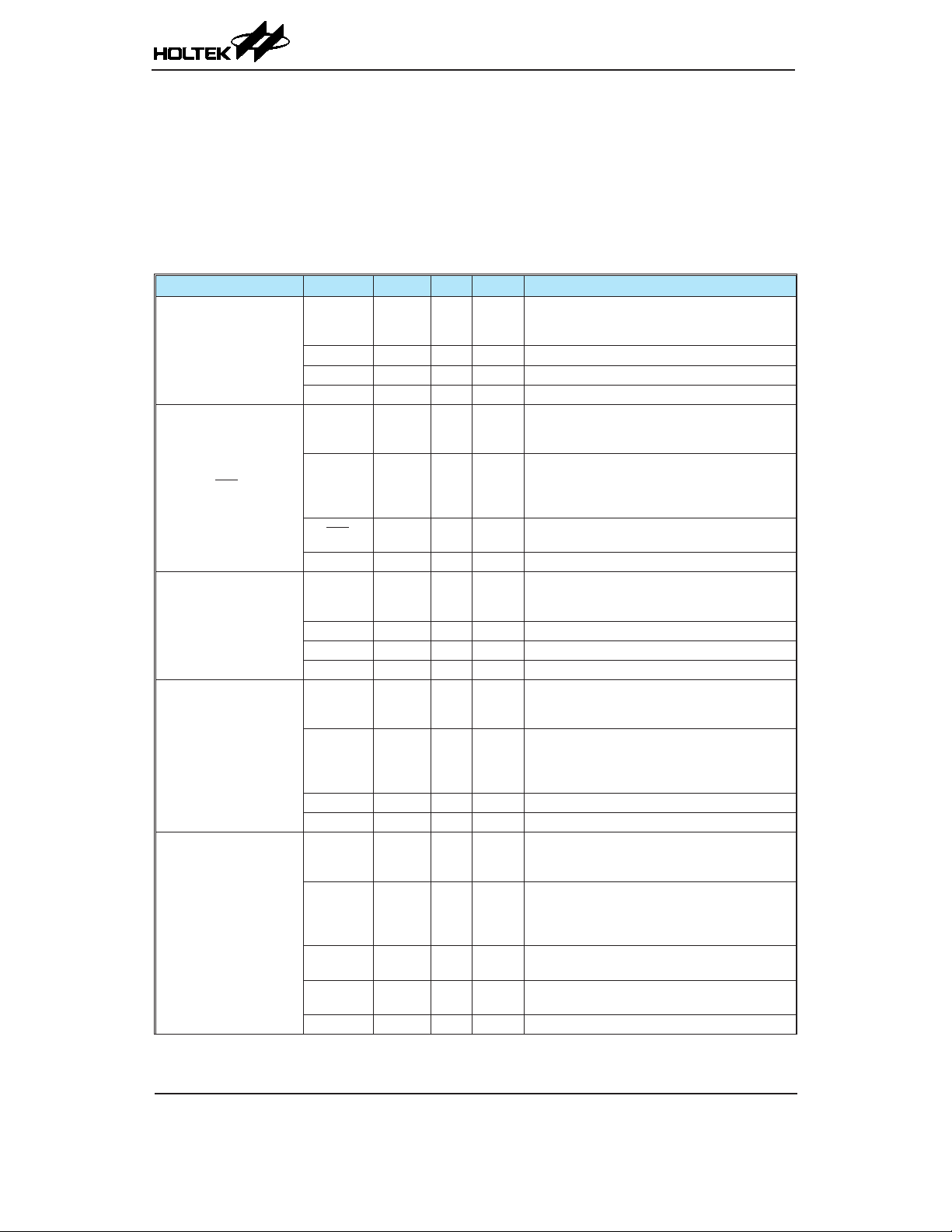
Pin Descriptions
With the exception of the power pins, all pins on these devices can be referenced by their Port name,
e.g. PA0, PA1, etc., which refer to the digital I/O function of the pins. However these Port pins are
also shared with other function such as the Analog to Digital Converter, Timer Module pins, etc.
The function of each pin is listed in the following table, however the details behind how each pin is
congured is contained in other sections of the datasheet.
HT67F2350
Pad Name Function OPT I/T O/T Description
PA0/SEG30/ICPDA/
OCDSDA
PA1/INT0/SCS/SEG26
PA2/SEG29/ICPCK/
OCDSCK
PA3/INT1/SDO/SEG25
PA4/INT2/SDI/SDA/
SEG24
PA0
SEG30 PAS0 — LCD LCD segment output
ICPDA — ST CMOS ICP Data/Address pin
OCDSDA — ST CMOS OCDS Data/Address pin, for EV chip only.
PA1
INT0
SCS
SEG26 PAS0 — LCD LCD segment output
PA2
SEG29 PAS0 — LCD LCD segment output
ICPCK — ST CMOS ICP Clock pin
OCDSCK — ST — OCDS Clock pin, for EV chip only.
PA3
INT1
SDO PAS0 — CMOS SPI data output
SEG25 PAS0 — LCD LCD segment output
PA4
INT2
SDI
SDA
SEG24 PAS1 — LCD LCD segment output
PAWU
PAPU
PAS0
PAWU
PAPU
PAS0
PAS0
INTEG
INTC0
IFS2
PAS0
IFS2
PAWU
PAPU
PAS0
PAWU
PAPU
PAS0
PAS0
INTEG
INTC0
IFS2
PAWU
PAPU
PAS1
PAS1
INTEG
INTC3
IFS2
PAS1
IFS2
PAS1
IFS2
ST CMOS
ST CMOS
ST — External Interrupt 0
ST CMOS SPI slave select
ST CMOS
ST CMOS
ST — External Interrupt 1
ST CMOS
ST — External Interrupt 2
ST — SPI data input
ST NMOS I2C data line
General purpose I/O. Register enabled pull-up
and wake-up.
General purpose I/O. Register enabled pull-up
and wake-up.
General purpose I/O. Register enabled pull-up
and wake-up.
General purpose I/O. Register enabled pull-up
and wake-up.
General purpose I/O. Register enabled pull-up
and wake-up.
Rev. 1.60 14 May 16, 2019 Rev. 1.60 15 May 16, 2019
Page 15
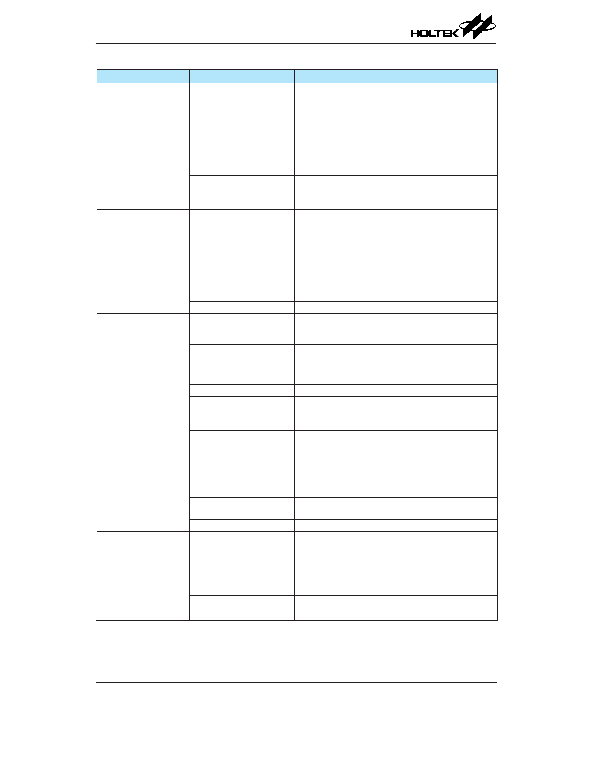
HT67F2350/HT67F2360
HT67F2370/HT67F2390
Advanced A/D Flash MCU with LCD & EEPROM
Pad Name Function OPT I/T O/T Description
PA5/INT3/SCK/SCL/
SEG23
PA6/INT0/RX0/SEG22
PA7/INT1/TX0/SEG21
PB0/STCK2/C0X/SEG32
PB1/PTCK3/SEG31
PB2/PTP3I/PTCK2/
PTP3/SEG16
PA5
INT3
SCK
SCL
SEG23 PAS1 — LCD LCD segment output
PA6
INT0
RX0
SEG22 PAS1 — LCD LCD segment output
PA7
INT1
TX0 PAS1 — CMOS UART0 TX serial data output
SEG21 PAS1 — LCD LCD segment output
PB0
STCK2
C0X PBS0 — CMOS Comparator 0 output
SEG32 PBS0 — LCD LCD segment output
PB1
PTCK3
SEG31 PBS0 — LCD LCD segment output
PB2
PTP3I
PTCK2
PTP3 PBS0 — CMOS PTM3 output
SEG16 PBS0 — LCD LCD segment output
PAWU
PAPU
PAS1
PAS1
INTEG
INTC3
IFS2
PAS1
IFS2
PAS1
IFS2
PAWU
PAPU
PAS1
PAS1
INTEG
INTC0
IFS2
PAS1
IFS4
PAWU
PAPU
PAS1
PAS1
INTEG
INTC0
IFS2
PBPU
PBS0
PBS0
IFS0
PBPU
PBS0
PBS0
IFS0
PBPU
PBS0
PBS0
IFS1
PBS0
IFS0
ST CMOS
ST — External Interrupt 3
ST CMOS SPI serial clock
ST NMOS I2C clock line
ST CMOS
ST — External Interrupt 0
ST — UART0 RX serial data input
ST CMOS
ST — External Interrupt 1
ST CMOS General purpose I/O. Register enabled pull-up.
ST — STM2 clock input
ST CMOS General purpose I/O. Register enabled pull-up.
ST — PTM3 clock input
ST CMOS General purpose I/O. Register enabled pull-up.
ST — PTM3 capture input
ST — PTM2 clock input
General purpose I/O. Register enabled pull-up
and wake-up.
General purpose I/O. Register enabled pull-up
and wake-up.
General purpose I/O. Register enabled pull-up
and wake-up.
Page 16
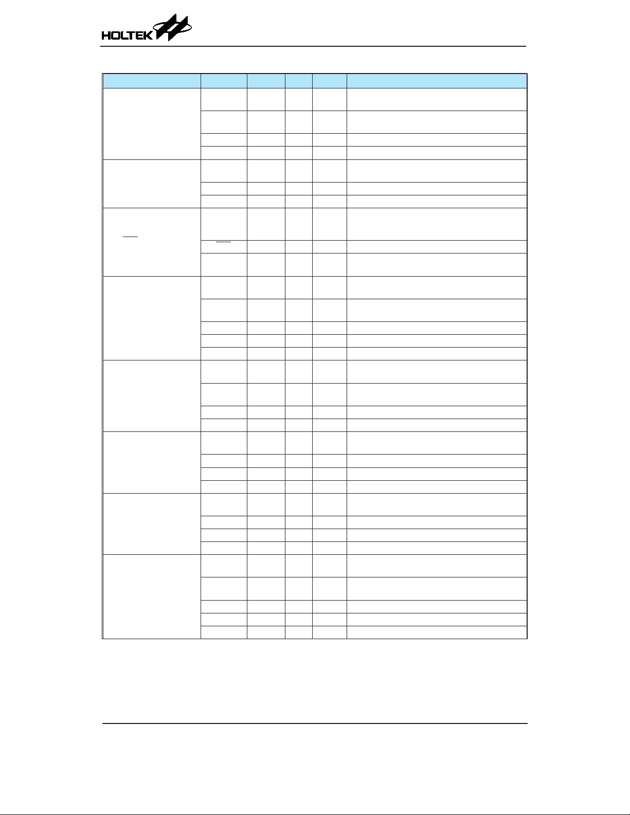
HT67F2350/HT67F2360
HT67F2370/HT67F2390
Advanced A/D Flash MCU with LCD & EEPROM
Pad Name Function OPT I/T O/T Description
PBPU
PBS0
PBS0
IFS1
PBPU
PBS1
PBPU
PBS1
RSTC
PBS1
RSTC
PBPU
PBS1
PBS1
IFS1
PBPU
PBS1
PBS1
IFS0
PCPU
PCS0
PCPU
PCS0
PCPU
PCS0
PCS0
IFS1
ST CMOS General purpose I/O. Register enabled pull-up.
ST — PTM2 capture input
ST CMOS General purpose I/O. Register enabled pull-up.
ST CMOS General purpose I/O. Register enabled pull-up.
— LCD LCD segment output
ST CMOS General purpose I/O. Register enabled pull-up.
ST — STM1 capture input
ST CMOS General purpose I/O. Register enabled pull-up.
ST — STM1 clock input
ST CMOS General purpose I/O. Register enabled pull-up.
ST CMOS General purpose I/O. Register enabled pull-up.
ST CMOS General purpose I/O. Register enabled pull-up.
ST — PTM0 capture input
PB3/PTP2I/PTP2/SEG27
PB4/C1X/SEG28
PB5/RES/SEG36
PB6/STP1I/STP1/OSC1/
SEG35
PB7/STCK1/OSC2/
SEG34
PC0/VREFI/AN0/SEG52
PC1/C0X/VREF/AN1
PC2/PTP0I/PTP0/AN2/
SEG51
PB3
PTP2I
PTP2 PBS0 — CMOS PTM2 output
SEG27 PBS0 — LCD LCD segment output
PB4
C1X PBS1 — CMOS Comparator 1 output
SEG28 PBS1 — LCD LCD segment output
PB5
RES RSTC ST — External reset input
SEG36
PB6
STP1I
STP1 PBS1 — CMOS STM1 output
OSC1 PBS1 HXT — HXT oscillator pin
SEG35 PBS1 — LCD LCD segment output
PB7
STCK1
OSC2 PBS1 — HXT HXT oscillator pin
SEG34 PBS1 — LCD LCD segment output
PC0
VREFI PCS0 AN — A/D Converter reference voltage input
AN0 PCS0 AN — A/D Converter analog input
SEG52 PCS0 — LCD LCD segment output
PC1
C0X PCS0 — CMOS Comparator 0 output
VREF PCS0 AN — A/D Converter reference voltage input
AN1 PCS0 AN — A/D Converter analog input
PC2
PTP0I
PTP0 PCS0 — CMOS PTM0 output
AN2 PCS0 AN — A/D Converter analog input
SEG51 PCS0 — LCD LCD segment output
Rev. 1.60 16 May 16, 2019 Rev. 1.60 17 May 16, 2019
Page 17
HT67F2350/HT67F2360
HT67F2370/HT67F2390
Advanced A/D Flash MCU with LCD & EEPROM
Pad Name Function OPT I/T O/T Description
PCPU
PCS0
PCS0
IFS0
PCPU
PCS1
PCS1
IFS1
PCPU
PCS1
PCS1
IFS0
PCPU
PCS1
PCS1
IFS1
PCPU
PCS1
PCS1
INTEG
INTC3
IFS2
PCS1
IFS0
ST CMOS General purpose I/O. Register enabled pull-up.
ST — PTM0 clock input
ST CMOS General purpose I/O. Register enabled pull-up.
ST — PTM1 capture input
ST CMOS General purpose I/O. Register enabled pull-up.
ST — PTM1 clock input
ST CMOS General purpose I/O. Register enabled pull-up.
ST — STM0 capture input
ST CMOS General purpose I/O. Register enabled pull-up.
ST — External Interrupt 3
ST — STM0 clock input
PC3/PTCK0/PTP4I/
PTP4/AN3/SEG50
PC4/PTP1I/PTP1/AN4/
SEG49
PC5/PTCK1/PTP5I/
PTP5/AN5/SEG48
PC6/STP0I/STP0/AN6/
SEG47
PC7/INT3/STCK0/PTP6I/
PTP6/AN7/SEG46
PC3
PTCK0
PTP4I PCS0 ST — PTM4 capture input
PTP4 PCS0 — CMOS PTM4 output
AN3 PCS0 AN — A/D Converter analog input
SEG50 PCS0 — LCD LCD segment output
PC4
PTP1I
PTP1 PCS1 — CMOS PTM1 output
AN4 PCS1 AN — A/D Converter analog input
SEG49 PCS1 — LCD LCD segment output
PC5
PTCK1
PTP5I PCS1 ST — PTM5 capture input
PTP5 PCS1 — CMOS PTM5 output
AN5 PCS1 AN — A/D Converter analog input
SEG48 PCS1 — LCD LCD segment output
PC6
STP0I
STP0 PCS1 — CMOS STM0 output
AN6 PCS1 AN — A/D Converter analog input
SEG47 PCS1 — LCD LCD segment output
PC7
INT3
STCK0
PTP6I PCS1 ST — PTM6 capture input
PTP6 PCS1 — CMOS PTM6 output
AN7 PCS1 AN — A/D Converter analog input
SEG46 PCS1 — LCD LCD segment output
Page 18
HT67F2350/HT67F2360
HT67F2370/HT67F2390
Advanced A/D Flash MCU with LCD & EEPROM
Pad Name Function OPT I/T O/T Description
PDPU
PDS0
PDS0
INTEG
INTC3
IFS2
PDS0
IFS1
PDPU
PDS0
PDS0
IFS0
PDS0
IFS4
PDPU
PDS0
PDS0
IFS1
PDPU
PDS0
PDS0
IFS0
PDPU
PDS1
PDS1
IFS1
PDS1
IFS4
PDPU
PDS1
PDS1
IFS0
ST CMOS General purpose I/O. Register enabled pull-up.
ST — External Interrupt 2
ST — STM1 capture input
ST CMOS General purpose I/O. Register enabled pull-up.
ST — STM1 clock input
ST — UART1 RX serial data input
ST CMOS General purpose I/O. Register enabled pull-up.
ST — PTM2 capture input
ST CMOS General purpose I/O. Register enabled pull-up.
ST — PTM2 clock input
ST CMOS General purpose I/O. Register enabled pull-up.
ST — PTM3 capture input
ST — UART0 RX serial data input
ST CMOS General purpose I/O. Register enabled pull-up.
ST — PTM3 clock input
PD0/INT2/STP1I/STP1/
AN8/SEG45
PD1/STCK1/RX1/AN9/
SEG44
PD2/PTP2I/PTP2/TX1/
AN10
PD3/PTCK2/PTP7I/
PTP7/AN11/SEG43
PD4/PTP3I/PTP3/RX0/
C1−
PD5/PTCK3/TX0/C1+/
SEG38
PD0
INT2
STP1I
STP1 PDS0 — CMOS STM1 output
AN8 PDS0 AN — A/D Converter analog input
SEG45 PCS1 — LCD LCD segment output
PD1
STCK1
RX1
AN9 PDS0 AN — A/D Converter analog input
SEG44 PDS0 — LCD LCD segment output
PD2
PTP2I
PTP2 PDS0 — CMOS PTM2 output
TX1 PDS0 — CMOS UART1 TX serial data output
AN10 PDS0 AN — A/D Converter analog input
PD3
PTCK2
PTP7I PDS0 ST — PTM7 capture input
PTP7 PDS0 — CMOS PTM7 output
AN11 PDS0 AN — A/D Converter analog input
SEG43 PDS0 — LCD LCD segment output
PD4
PTP3I
PTP3 PDS1 — CMOS PTM3 output
RX0
C1− PDS1 AN — Comparator 1 negative input
PD5
PTCK3
TX0 PDS1 — CMOS UART0 TX serial data output
C1+ PDS1 AN — Comparator 1 positive input
SEG38 PDS1 — LCD LCD segment output
Rev. 1.60 18 May 16, 2019 Rev. 1.60 19 May 16, 2019
Page 19
HT67F2350/HT67F2360
HT67F2370/HT67F2390
Advanced A/D Flash MCU with LCD & EEPROM
Pad Name Function OPT I/T O/T Description
PD6
PD6/STP2I/STP2/C1X/
SEG33
PE0/STCK0/SCSA/SEG7
PE1/STP0I/STP0/SDOA/
SEG6
PE2/PTCK1/SDIA/SEG5
PE3/PTP1I/PTP1/SCKA/
SEG4
PE4 PE4
PE5/C2/SEG55
PE6/C1/SEG54
PE7/V2/SEG53
PF0/SCS/SEG15
STP2I
STP2 PDS1 — CMOS STM2 output
C1X PDS1 — CMOS Comparator 1 output
SEG33 PDS1 — LCD LCD segment output
PE0
STCK0
SCSA PES0 ST CMOS SPIA slave select
SEG7 PES0 — LCD LCD segment output
PE1
STP0I
STP0 PES0 — CMOS STM0 inverted output
SDOA PES0 — CMOS SPIA data output
SEG6 PES0 — LCD LCD segment output
PE2
PTCK1
SDIA PES0 ST — SPIA data input
SEG5 PES0 — LCD LCD segment output
PE3
PTP1I
PTP1 PES0 — CMOS PTM1 output
SCKA PES0 ST CMOS SPIA serial clock
SEG4 PES0 — LCD LCD segment output
PE5
C2 PES1 — AN LCD voltage pump
SEG55 PES1 — LCD LCD segment output
PE6
C1 PES1 — AN LCD voltage pump
SEG54 PES1 — LCD LCD segment output
PE7
V2 PES1 PWR AN LCD voltage pump
SEG53 PES1 — LCD LCD segment output
PF0
SCS
SEG15 PFS0 — LCD LCD segment output
PDPU
PDS1
PDS1
IFS1
PEPU
PES0
PES0
IFS0
PEPU
PES0
PES0
IFS1
PEPU
PES0
PES0
IFS0
PEPU
PES0
PES0
IFS1
PEPU
PES1
PEPU
PES1
PEPU
PES1
PEPU
PES1
PFPU
PFS0
PFS0
IFS2
ST CMOS General purpose I/O. Register enabled pull-up.
ST — STM2 capture input
ST CMOS General purpose I/O. Register enabled pull-up.
ST — STM0 clock input
ST CMOS General purpose I/O. Register enabled pull-up.
ST — STM0 capture input
ST CMOS General purpose I/O. Register enabled pull-up.
ST — PTM1 clock input
ST CMOS General purpose I/O. Register enabled pull-up.
ST — PTM1 capture input
ST CMOS General purpose I/O. Register enabled pull-up.
ST CMOS General purpose I/O. Register enabled pull-up.
ST CMOS General purpose I/O. Register enabled pull-up.
ST CMOS General purpose I/O. Register enabled pull-up.
ST CMOS General purpose I/O. Register enabled pull-up.
ST CMOS SPI slave select
Page 20

HT67F2350/HT67F2360
HT67F2370/HT67F2390
Advanced A/D Flash MCU with LCD & EEPROM
Pad Name Function OPT I/T O/T Description
PFPU
PFS0
PFPU
PFS0
PFS0
IFS2
PFS0
IFS2
PFPU
PFS0
PFS0
IFS2
PFS0
IFS2
PFPU
PFS1
PFS1
IFS0
PFPU
PFS1
PFS1
IFS1
PFPU
PFS1
PFS1
IFS0
PFS1
IFS4
PFPU
PFS1
PFS1
IFS1
PGPU
PGS1
PGPU
PGS1
PGPU
PGS1
ST CMOS General purpose I/O. Register enabled pull-up.
ST CMOS General purpose I/O. Register enabled pull-up.
ST — SPI data input
ST NMOS I2C data line
ST CMOS General purpose I/O. Register enabled pull-up.
ST CMOS SPI serial clock
ST NMOS I2C clock line
ST CMOS General purpose I/O. Register enabled pull-up.
ST — PTM0 clock input
ST CMOS General purpose I/O. Register enabled pull-up.
ST — PTM0 capture input
ST CMOS General purpose I/O. Register enabled pull-up.
ST — STM2 clock input
ST — UART1 RX serial data input
ST CMOS General purpose I/O. Register enabled pull-up.
ST — STM2 capture input
ST CMOS General purpose I/O. Register enabled pull-up.
ST CMOS General purpose I/O. Register enabled pull-up.
ST CMOS General purpose I/O. Register enabled pull-up.
PF1/SDO/SEG14
PF2/SDI/SDA/SEG13
PF3/SCK/SCL/SEG12
PF4/PTCK0/XT2
PF5/PTP0I/PTP0/XT1
PF6/STCK2/RX1/C0−/
SEG37
PF7/STP2I/STP2/TX1/
C0+
PG4/COM0
PG5/COM1
PG6/COM2
PF1
SDO PFS0 — CMOS SPI data output
SEG14 PFS0 — LCD LCD segment output
PF2
SDI
SDA
SEG13 PFS0 — LCD LCD segment output
PF3
SCK
SCL
SEG12 PFS0 — LCD LCD segment output
PF4
PTCK0
XT2 PFS1 — LXT LXT oscillator pin
PF5
PTP0I
PTP0 PFS1 — CMOS PTM0 output
XT1 PFS1 LXT — LXT oscillator pin
PF6
STCK2
RX1
C0− PFS1 AN — Comparator 0 negative input
SEG37 PFS1 — LCD LCD segment output
PF7
STP2I
STP2 PFS1 — CMOS STM2 output
TX1 PFS1 — CMOS UART1 TX serial data output
C0+ PFS1 AN — Comparator 0 positive input
PG4
COM0 PGS1 — LCD LCD common output
PG5
COM1 PGS1 — LCD LCD common output
PG6
COM2 PGS1 — LCD LCD common output
Rev. 1.60 20 May 16, 2019 Rev. 1.60 21 May 16, 2019
Page 21
HT67F2350/HT67F2360
HT67F2370/HT67F2390
Advanced A/D Flash MCU with LCD & EEPROM
Pad Name Function OPT I/T O/T Description
PG7/COM3
PJ0/COM4/SEG0
PJ1/COM5/SEG1
PJ2/COM6/SEG2
PJ3/COM7/SEG3
PJ6/PTCK5/SEG10
PJ7/PTCK4/SEG11
VDD VDD — PWR — Positive power supply
VSS VSS — PWR — Negative power supply, ground.
AVDD AVDD — PWR — Analog positive power supply
AVSS AVSS — PWR — Analog negative power supply, ground.
VMAX VMAX — PWR — IC maximum voltage, connected to VDD or V1.
V1 V1 — PWR AN LCD voltage pump
PLCD PLCD — PWR AN LCD power supply
PG7
COM3 PGS1 — LCD LCD common output
PJ0
COM4 PJS0 — LCD LCD common output
SEG0 PJS0 — LCD LCD segment output
PJ1
COM5 PJS0 — LCD LCD common output
SEG1 PJS0 — LCD LCD segment output
PJ2
COM6 PJS0 — LCD LCD common output
SEG2 PJS0 — LCD LCD segment output
PJ3
COM7 PJS0 — LCD LCD common output
SEG3 PJS0 — LCD LCD segment output
PJ6
PTCK5 PJS1 ST — PTM5 clock input
SEG10 PJS1 — LCD LCD segment output
PJ7
PTCK4 PJS1 ST — PTM4 clock input
SEG11 PJS1 — LCD LCD segment output
Legend: I/T: Input type; O/T: Output type; OPT: Optional by register option;
CMOS: CMOS output; NMOS: NMOS output;
ST: Schmitt Trigger input; AN: Analog signal;
HXT: High frequency crystal oscillator; LXT: Low frequency crystal oscillator;
LCD: LCD SEG/COM output; PWR: Power
PGPU
PGS1
PJPU
PJS0
PJPU
PJS0
PJPU
PJS0
PJPU
PJS0
PJPU
PJS1
PJPU
PJS1
ST CMOS General purpose I/O. Register enabled pull-up.
ST CMOS General purpose I/O. Register enabled pull-up.
ST CMOS General purpose I/O. Register enabled pull-up.
ST CMOS General purpose I/O. Register enabled pull-up.
ST CMOS General purpose I/O. Register enabled pull-up.
ST CMOS General purpose I/O. Register enabled pull-up.
ST CMOS General purpose I/O. Register enabled pull-up.
Page 22
HT67F2350/HT67F2360
HT67F2370/HT67F2390
Advanced A/D Flash MCU with LCD & EEPROM
HT67F2360
Pad Name Function OPT I/T O/T Description
PA0/SEG30/ICPDA/
OCDSDA
PA1/INT0/SCS/SEG26
PA2/SEG29/ICPCK/
OCDSCK
PA3/INT1/SDO/SEG25
PA4/INT2/SDI/SDA/
SEG24
PA0
SEG30 PAS0 — LCD LCD segment output
ICPDA — ST CMOS ICP Data/Address pin
OCDSDA — ST CMOS OCDS Data/Address pin, for EV chip only.
PA1
INT0
SCS
SEG26 PAS0 — LCD LCD segment output
PA2
SEG29 PAS0 — LCD LCD segment output
ICPCK — ST CMOS ICP Clock pin
OCDSCK — ST — OCDS Clock pin, for EV chip only.
PA3
INT1
SDO PAS0 — CMOS SPI data output
SEG25 PAS0 — LCD LCD segment output
PA4
INT2
SDI
SDA
SEG24 PAS1 — LCD LCD segment output
PAWU
PAPU
PAS0
PAWU
PAPU
PAS0
PAS0
INTEG
INTC0
IFS2
PAS0
IFS2
PAWU
PAPU
PAS0
PAWU
PAPU
PAS0
PAS0
INTEG
INTC0
IFS2
PAWU
PAPU
PAS1
PAS1
INTEG
INTC3
IFS2
PAS1
IFS2
PAS1
IFS2
ST CMOS
ST CMOS
ST — External Interrupt 0
ST CMOS SPI slave select
ST CMOS
ST CMOS
ST — External Interrupt 1
ST CMOS
ST — External Interrupt 2
ST — SPI data input
ST NMOS I2C data line
General purpose I/O. Register enabled pull-up
and wake-up.
General purpose I/O. Register enabled pull-up
and wake-up.
General purpose I/O. Register enabled pull-up
and wake-up.
General purpose I/O. Register enabled pull-up
and wake-up.
General purpose I/O. Register enabled pull-up
and wake-up.
Rev. 1.60 22 May 16, 2019 Rev. 1.60 23 May 16, 2019
Page 23

HT67F2350/HT67F2360
HT67F2370/HT67F2390
Advanced A/D Flash MCU with LCD & EEPROM
Pad Name Function OPT I/T O/T Description
PA5/INT3/SCK/SCL/
SEG23
PA6/INT0/RX0/SEG22
PA7/INT1/TX0/SEG21
PB0/STCK2/C0X/SEG32
PB1/PTCK3/SEG31
PB2/PTP3I/PTCK2/PTP3/
SEG16
PA5
INT3
SCK
SCL
SEG23 PAS1 — LCD LCD segment output
PA6
INT0
RX0
SEG22 PAS1 — LCD LCD segment output
PA7
INT1
TX0 PAS1 — CMOS UART0 TX serial data output
SEG21 PAS1 — LCD LCD segment output
PB0
STCK2
C0X PBS0 — CMOS Comparator 0 output
SEG32 PBS0 — LCD LCD segment output
PB1
PTCK3
SEG31 PBS0 — LCD LCD segment output
PB2
PTP3I
PTCK2
PTP3 PBS0 — CMOS PTM3 output
SEG16 PBS0 — LCD LCD segment output
PAWU
PAPU
PAS1
PAS1
INTEG
INTC3
IFS2
PAS1
IFS2
PAS1
IFS2
PAWU
PAPU
PAS1
PAS1
INTEG
INTC0
IFS2
PAS1
IFS4
PAWU
PAPU
PAS1
PAS1
INTEG
INTC0
IFS2
PBPU
PBS0
PBS0
IFS0
PBPU
PBS0
PBS0
IFS0
PBPU
PBS0
PBS0
IFS1
PBS0
IFS0
ST CMOS
ST — External Interrupt 3
ST CMOS SPI serial clock
ST NMOS I2C clock line
ST CMOS
ST — External Interrupt 0
ST — UART0 RX serial data input
ST CMOS
ST — External Interrupt 1
ST CMOS General purpose I/O. Register enabled pull-up.
ST — STM2 clock input
ST CMOS General purpose I/O. Register enabled pull-up.
ST — PTM3 clock input
ST CMOS General purpose I/O. Register enabled pull-up.
ST — PTM3 capture input
ST — PTM2 clock input
General purpose I/O. Register enabled pull-up
and wake-up.
General purpose I/O. Register enabled pull-up
and wake-up.
General purpose I/O. Register enabled pull-up
and wake-up.
Page 24

HT67F2350/HT67F2360
HT67F2370/HT67F2390
Advanced A/D Flash MCU with LCD & EEPROM
Pad Name Function OPT I/T O/T Description
PBPU
PBS0
PBS0
IFS1
PBPU
PBS1
PBPU
PBS1
RSTC
PBPU
PBS1
PBS1
IFS1
PBPU
PBS1
PBS1
IFS0
PCPU
PCS0
PCPU
PCS0
PCPU
PCS0
PCS0
IFS1
ST CMOS General purpose I/O. Register enabled pull-up.
ST — PTM2 capture input
ST CMOS General purpose I/O. Register enabled pull-up.
ST CMOS General purpose I/O. Register enabled pull-up.
ST CMOS General purpose I/O. Register enabled pull-up.
ST — STM1 capture input
ST CMOS General purpose I/O. Register enabled pull-up.
ST — STM1 clock input
ST CMOS General purpose I/O. Register enabled pull-up.
ST CMOS General purpose I/O. Register enabled pull-up.
ST CMOS General purpose I/O. Register enabled pull-up.
ST — PTM0 capture input
PB3/PTP2I/PTP2/SEG27
PB4/C1X/SEG28
PB5/RES/SEG36
PB6/STP1I/STP1/OSC1/
SEG35
PB7/STCK1/OSC2/
SEG34
PC0/VREFI/AN0/SEG52
PC1/C0X/VREF/AN1
PC2/PTP0I/PTP0/AN2/
SEG51
PB3
PTP2I
PTP2 PBS0 — CMOS PTM2 output
SEG27 PBS0 — LCD LCD segment output
PB4
C1X PBS1 — CMOS Comparator 1 output
SEG28 PBS1 — LCD LCD segment output
PB5
RES RSTC ST — External reset input
SEG36 PBS1 — LCD LCD segment output
PB6
STP1I
STP1 PBS1 — CMOS STM1 output
OSC1 PBS1 HXT — HXT oscillator pin
SEG35 PBS1 — LCD LCD segment output
PB7
STCK1
OSC2 PBS1 — HXT HXT oscillator pin
SEG34 PBS1 — LCD LCD segment output
PC0
VREFI PCS0 AN — A/D Converter reference voltage input
AN0 PCS0 AN — A/D Converter analog input
SEG52 PCS0 — LCD LCD segment output
PC1
C0X PCS0 — CMOS Comparator 0 output
VREF PCS0 AN — A/D Converter reference voltage input
AN1 PCS0 AN — A/D Converter analog input
PC2
PTP0I
PTP0 PCS0 — CMOS PTM0 output
AN2 PCS0 AN — A/D Converter analog input
SEG51 PCS0 — LCD LCD segment output
Rev. 1.60 24 May 16, 2019 Rev. 1.60 25 May 16, 2019
Page 25
HT67F2350/HT67F2360
HT67F2370/HT67F2390
Advanced A/D Flash MCU with LCD & EEPROM
Pad Name Function OPT I/T O/T Description
PCPU
PCS0
PCS0
IFS0
PCS0
IFS3
PCPU
PCS1
PCS1
IFS1
PCPU
PCS1
PCS1
IFS0
PCS1
IFS3
PCPU
PCS1
PCS1
IFS1
PCPU
PCS1
PCS1
INTEG
INTC3
IFS2
PCS1
IFS0
PCS1
IFS3
ST CMOS General purpose I/O. Register enabled pull-up.
ST — PTM0 clock input
ST — PTM4 capture input
ST CMOS General purpose I/O. Register enabled pull-up.
ST — PTM1 capture input
ST CMOS General purpose I/O. Register enabled pull-up.
ST — PTM1 clock input
ST — PTM5 capture input
ST CMOS General purpose I/O. Register enabled pull-up.
ST — STM0 capture input
ST CMOS General purpose I/O. Register enabled pull-up.
ST — External Interrupt 3
ST — STM0 clock input
ST — PTM6 capture input
PC3/PTCK0/PTP4I/
PTP4/AN3/SEG50
PC4/PTP1I/PTP1/AN4/
SEG49
PC5/PTCK1/PTP5I/
PTP5/AN5/SEG48
PC6/STP0I/STP0/AN6/
SEG47
PC7/INT3/STCK0/PTP6I/
PTP6/AN7/SEG46
PC3
PTCK0
PTP4I
PTP4 PCS0 — CMOS PTM4 output
AN3 PCS0 AN — A/D Converter analog input
SEG50 PCS0 — LCD LCD segment output
PC4
PTP1I
PTP1 PCS1 — CMOS PTM1 output
AN4 PCS1 AN — A/D Converter analog input
SEG49 PCS1 — LCD LCD segment output
PC5
PTCK1
PTP5I
PTP5 PCS1 — CMOS PTM5 output
AN5 PCS1 AN — A/D Converter analog input
SEG48 PCS1 — LCD LCD segment output
PC6
STP0I
STP0 PCS1 — CMOS STM0 output
AN6 PCS1 AN — A/D Converter analog input
SEG47 PCS1 — LCD LCD segment output
PC7
INT3
STCK0
PTP6I
PTP6 PCS1 — CMOS PTM6 output
AN7 PCS1 AN — A/D Converter analog input
SEG46 PCS1 — LCD LCD segment output
Page 26
HT67F2350/HT67F2360
HT67F2370/HT67F2390
Advanced A/D Flash MCU with LCD & EEPROM
Pad Name Function OPT I/T O/T Description
PDPU
PDS0
PDS0
INTEG
INTC3
IFS2
PDS0
IFS1
PDPU
PDS0
PDS0
IFS0
PDS0
IFS4
PDPU
PDS0
PDS0
IFS1
PDPU
PDS0
PDS0
IFS0
PDS0
IFS3
PDPU
PDS1
PDS1
IFS1
PDS1
IFS4
PDPU
PDS1
PDS1
IFS0
ST CMOS General purpose I/O. Register enabled pull-up.
ST — External Interrupt 2
ST — STM1 capture input
ST CMOS General purpose I/O. Register enabled pull-up.
ST — STM1 clock input
ST — UART1 RX serial data input
ST CMOS General purpose I/O. Register enabled pull-up.
ST — PTM2 capture input
ST CMOS General purpose I/O. Register enabled pull-up.
ST — PTM2 clock input
ST — PTM7 capture input
ST CMOS General purpose I/O. Register enabled pull-up.
ST — PTM3 capture input
ST — UART0 RX serial data input
ST CMOS General purpose I/O. Register enabled pull-up.
ST — PTM3 clock input
PD0/INT2/STP1I/STP1/
AN8/SEG45
PD1/STCK1/RX1/AN9/
SEG44
PD2/PTP2I/PTP2/TX1/
AN10
PD3/PTCK2/PTP7I/
PTP7/AN11/SEG43
PD4/PTP3I/PTP3/RX0/
C1−
PD5/PTCK3/TX0/C1+/
SEG38
PD0
INT2
STP1I
STP1 PDS0 — CMOS STM1 output
AN8 PDS0 AN — A/D Converter analog input
SEG45 PCS1 — LCD LCD segment output
PD1
STCK1
RX1
AN9 PDS0 AN — A/D Converter analog input
SEG44 PDS0 — LCD LCD segment output
PD2
PTP2I
PTP2 PDS0 — CMOS PTM2 output
TX1 PDS0 — CMOS UART1 TX serial data output
AN10 PDS0 AN — A/D Converter analog input
PD3
PTCK2
PTP7I
PTP7 PDS0 — CMOS PTM7 output
AN11 PDS0 AN — A/D Converter analog input
SEG43 PDS0 — LCD LCD segment output
PD4
PTP3I
PTP3 PDS1 — CMOS PTM3 output
RX0
C1− PDS1 AN — Comparator 1 negative input
PD5
PTCK3
TX0 PDS1 — CMOS UART0 TX serial data output
C1+ PDS1 AN — Comparator 1 positive input
SEG38 PDS1 — LCD LCD segment output
Rev. 1.60 26 May 16, 2019 Rev. 1.60 27 May 16, 2019
Page 27

HT67F2350/HT67F2360
HT67F2370/HT67F2390
Advanced A/D Flash MCU with LCD & EEPROM
Pad Name Function OPT I/T O/T Description
PD6
PD6/STP2I/STP2/C1X/
SEG33
PE0/STCK0/SCSA/SEG7
PE1/STP0I/STP0/SDOA/
SEG6
PE2/PTCK1/SDIA/SEG5
PE3/PTP1I/PTP1/SCKA/
SEG4
PE4 PE4
PE5/C2/SEG55
PE6/C1/SEG54
PE7/V2/SEG53
PF0/SCS/SEG15
STP2I
STP2 PDS1 — CMOS STM2 output
C1X PDS1 — CMOS Comparator 1 output
SEG33 PDS1 — LCD LCD segment output
PE0
STCK0
SCSA PES0 ST CMOS SPIA slave select
SEG7 PES0 — LCD LCD segment output
PE1
STP0I
STP0 PES0 — CMOS STM0 inverted output
SDOA PES0 — CMOS SPIA data output
SEG6 PES0 — LCD LCD segment output
PE2
PTCK1
SDIA PES0 ST — SPIA data input
SEG5 PES0 — LCD LCD segment output
PE3
PTP1I
PTP1 PES0 — CMOS PTM1 output
SCKA PES0 ST CMOS SPIA serial clock
SEG4 PES0 — LCD LCD segment output
PE5
C2 PES1 — AN LCD voltage pump
SEG55 PES1 — LCD LCD segment output
PE6
C1 PES1 — AN LCD voltage pump
SEG54 PES1 — LCD LCD segment output
PE7
V2 PES1 PWR AN LCD voltage pump
SEG53 PES1 — LCD LCD segment output
PF0
SCS
SEG15 PFS0 — LCD LCD segment output
PDPU
PDS1
PDS1
IFS1
PEPU
PES0
PES0
IFS0
PEPU
PES0
PES0
IFS1
PEPU
PES0
PES0
IFS0
PEPU
PES0
PES0
IFS1
PEPU
PES1
PEPU
PES1
PEPU
PES1
PEPU
PES1
PFPU
PFS0
PFS0
IFS2
ST CMOS General purpose I/O. Register enabled pull-up.
ST — STM2 capture input
ST CMOS General purpose I/O. Register enabled pull-up.
ST — STM0 clock input
ST CMOS General purpose I/O. Register enabled pull-up.
ST — STM0 capture input
ST CMOS General purpose I/O. Register enabled pull-up.
ST — PTM1 clock input
ST CMOS General purpose I/O. Register enabled pull-up.
ST — PTM1 capture input
ST CMOS General purpose I/O. Register enabled pull-up.
ST CMOS General purpose I/O. Register enabled pull-up.
ST CMOS General purpose I/O. Register enabled pull-up.
ST CMOS General purpose I/O. Register enabled pull-up.
ST CMOS General purpose I/O. Register enabled pull-up.
ST CMOS SPI slave select
Page 28

HT67F2350/HT67F2360
HT67F2370/HT67F2390
Advanced A/D Flash MCU with LCD & EEPROM
Pad Name Function OPT I/T O/T Description
PFPU
PFS0
PFPU
PFS0
PFS0
IFS2
PFS0
IFS2
PFPU
PFS0
PFS0
IFS2
PFS0
IFS2
PFPU
PFS1
PFS1
IFS0
PFPU
PFS1
PFS1
IFS1
PFPU
PFS1
PFS1
IFS0
PFS1
IFS4
PFPU
PFS1
PFS1
IFS1
PGPU
PGS0
PGPU
PGS0
ST CMOS General purpose I/O. Register enabled pull-up.
ST CMOS General purpose I/O. Register enabled pull-up.
ST — SPI data input
ST NMOS I2C data line
ST CMOS General purpose I/O. Register enabled pull-up.
ST CMOS SPI serial clock
ST NMOS I2C clock line
ST CMOS General purpose I/O. Register enabled pull-up.
ST — PTM0 clock input
ST CMOS General purpose I/O. Register enabled pull-up.
ST — PTM0 capture input
ST CMOS General purpose I/O. Register enabled pull-up.
ST — STM2 clock input
ST — UART1 RX serial data input
ST CMOS General purpose I/O. Register enabled pull-up.
ST — STM2 capture input
ST CMOS General purpose I/O. Register enabled pull-up.
ST CMOS General purpose I/O. Register enabled pull-up.
PF1/SDO/SEG14
PF2/SDI/SDA/SEG13
PF3/SCK/SCL/SEG12
PF4/PTCK0/XT2
PF5/PTP0I/PTP0/XT1
PF6/STCK2/RX1/C0−/
SEG37
PF7/STP2I/STP2/TX1/
C0+
PG0/COM0
PG1/COM1
PF1
SDO PFS0 — CMOS SPI data output
SEG14 PFS0 — LCD LCD segment output
PF2
SDI
SDA
SEG13 PFS0 — LCD LCD segment output
PF3
SCK
SCL
SEG12 PFS0 — LCD LCD segment output
PF4
PTCK0
XT2 PFS1 — LXT LXT oscillator pin
PF5
PTP0I
PTP0 PFS1 — CMOS PTM0 output
XT1 PFS1 LXT — LXT oscillator pin
PF6
STCK2
RX1
C0− PFS1 AN — Comparator 0 negative input
SEG37 PFS1 — LCD LCD segment output
PF7
STP2I
STP2 PFS1 — CMOS STM2 output
TX1 PFS1 — CMOS UART1 TX serial data output
C0+ PFS1 AN — Comparator 0 positive input
PG0
COM0 PGS0 — LCD LCD common output
PG1
COM1 PGS0 — LCD LCD common output
Rev. 1.60 28 May 16, 2019 Rev. 1.60 29 May 16, 2019
Page 29
HT67F2350/HT67F2360
HT67F2370/HT67F2390
Advanced A/D Flash MCU with LCD & EEPROM
Pad Name Function OPT I/T O/T Description
PGPU
PGS0
PGPU
PGS0
PGPU
PGS1
PGPU
PGS1
PGPU
PGS1
PGPU
PGS1
PHPU
PHS0
PHS0
IFS3
PHPU
PHS0
PHS0
IFS3
PHPU
PHS0
PHS0
IFS3
PHPU
PHS0
PHS0
IFS3
PHPU
PHS1
PHS1
IFS3
ST CMOS General purpose I/O. Register enabled pull-up.
ST CMOS General purpose I/O. Register enabled pull-up.
ST CMOS General purpose I/O. Register enabled pull-up.
ST CMOS General purpose I/O. Register enabled pull-up.
ST CMOS General purpose I/O. Register enabled pull-up.
ST CMOS General purpose I/O. Register enabled pull-up.
ST CMOS General purpose I/O. Register enabled pull-up.
ST — PTM4 capture input
ST CMOS General purpose I/O. Register enabled pull-up.
ST — PTM5 capture input
ST CMOS General purpose I/O. Register enabled pull-up.
ST — PTM4 clock input
ST CMOS General purpose I/O. Register enabled pull-up.
ST — PTM5 clock input
ST CMOS General purpose I/O. Register enabled pull-up.
ST — PTM6 clock input
PG2/COM2
PG3/COM3
PG4/COM0
PG5/COM1
PG6/COM2
PG7/COM3
PH0/PTP4I/PTP4/SEG20
PH1/PTP5I/PTP5/SEG19
PH2/PTCK4/AN12/
SEG42
PH3/PTCK5/AN13/
SEG41
PH4/PTCK6/AN14/
SEG40
PG2
COM2 PGS0 — LCD LCD common output
PG3
COM3 PGS0 — LCD LCD common output
PG4
COM0 PGS1 — LCD LCD common output
PG5
COM1 PGS1 — LCD LCD common output
PG6
COM2 PGS1 — LCD LCD common output
PG7
COM3 PGS1 — LCD LCD common output
PH0
PTP4I
PTP4 PHS0 — CMOS PTM4 output
SEG20 PHS0 — LCD LCD segment output
PH1
PTP5I
PTP5 PHS0 — CMOS PTM5 output
SEG19 PHS0 — LCD LCD segment output
PH2
PTCK4
AN12 PHS0 AN — A/D Converter analog input
SEG42 PHS0 — LCD LCD segment output
PH3
PTCK5
AN13 PHS0 AN — A/D Converter analog input
SEG41 PHS0 — LCD LCD segment output
PH4
PTCK6
AN14 PHS1 AN — A/D Converter analog input
SEG40 PHS1 — LCD LCD segment output
Page 30
HT67F2350/HT67F2360
HT67F2370/HT67F2390
Advanced A/D Flash MCU with LCD & EEPROM
Pad Name Function OPT I/T O/T Description
PHPU
PHS1
PHS1
IFS3
PHPU
PHS1
PHS1
IFS3
PHPU
PHS1
PHS1
IFS3
PJPU
PJS0
PJPU
PJS0
PJPU
PJS0
PJPU
PJS0
PJPU
PJS1
PJS1
IFS3
PJPU
PJS1
PJS1
IFS3
PJPU
PJS1
PJS1
IFS3
ST CMOS General purpose I/O. Register enabled pull-up.
ST — PTM7 clock input
ST CMOS General purpose I/O. Register enabled pull-up.
ST — PTM6 capture input
ST CMOS General purpose I/O. Register enabled pull-up.
ST — PTM7 capture input
ST CMOS General purpose I/O. Register enabled pull-up.
ST CMOS General purpose I/O. Register enabled pull-up.
ST CMOS General purpose I/O. Register enabled pull-up.
ST CMOS General purpose I/O. Register enabled pull-up.
ST CMOS General purpose I/O. Register enabled pull-up.
ST — PTM5 clock input
ST CMOS General purpose I/O. Register enabled pull-up.
ST — PTM4 clock input
ST CMOS General purpose I/O. Register enabled pull-up.
ST — PTM5 clock input
PH5/PTCK7/AN15/
SEG39
PH6/PTP6I/PTP6/SEG18
PH7/PTP7I/PTP7/SEG17
PJ0/COM4/SEG0
PJ1/COM5/SEG1
PJ2/COM6/SEG2
PJ3/COM7/SEG3
PJ4/PTCK7/SEG8
PJ5/PTCK6/SEG9
PJ6/PTCK5/SEG10
PH5
PTCK7
AN15 PHS1 AN — A/D Converter analog input
SEG39 PHS1 — LCD LCD segment output
PH6
PTP6I
PTP6 PHS1 — CMOS PTM6 output
SEG18 PHS1 — LCD LCD segment output
PH7
PTP7I
PTP7 PHS1 — CMOS PTM7 output
SEG17 PHS1 — LCD LCD segment output
PJ0
COM4 PJS0 — LCD LCD common output
SEG0 PJS0 — LCD LCD segment output
PJ1
COM5 PJS0 — LCD LCD common output
SEG1 PJS0 — LCD LCD segment output
PJ2
COM6 PJS0 — LCD LCD common output
SEG2 PJS0 — LCD LCD segment output
PJ3
COM7 PJS0 — LCD LCD common output
SEG3 PJS0 — LCD LCD segment output
PJ4
PTCK7
SEG8 PJS1 — LCD LCD segment output
PJ5
PTCK6
SEG9 PJS1 — LCD LCD segment output
PJ6
PTCK5
SEG10 PJS1 — LCD LCD segment output
Rev. 1.60 30 May 16, 2019 Rev. 1.60 31 May 16, 2019
Page 31

HT67F2350/HT67F2360
HT67F2370/HT67F2390
Advanced A/D Flash MCU with LCD & EEPROM
Pad Name Function OPT I/T O/T Description
PJ7
PJ7/PTCK4/SEG11
VDD VDD — PWR — Positive power supply
VSS VSS — PWR — Negative power supply, ground.
AVDD AVDD — PWR — Analog positive power supply
AVSS AVSS — PWR — Analog negative power supply, ground.
VMAX VMAX — PWR — IC maximum voltage, connected to VDD or V1.
V1 V1 — PWR AN LCD voltage pump
PLCD PLCD — PWR AN LCD power supply
PTCK4
SEG11 PJS1 — LCD LCD segment output
Legend: I/T: Input type; O/T: Output type; OPT: Optional by register option;
CMOS: CMOS output; NMOS: NMOS output;
ST: Schmitt Trigger input; AN: Analog signal;
HXT: High frequency crystal oscillator; LXT: Low frequency crystal oscillator;
LCD: LCD SEG/COM output; PWR: Power
HT67F2370/HT67F2390
Pad Name Function OPT I/T O/T Description
PA0
PA0/SEG30/ICPDA/
OCDSDA
PA1/INT0/SCS/SEG26
PA2/SEG29/ICPCK/
OCDSCK
PA3/INT1/SDO/SEG25
SEG30 PAS0 — LCD LCD segment output
ICPDA — ST CMOS ICP Data/Address pin
OCDSDA — ST CMOS OCDS Data/Address pin, for EV chip only.
PA1
INT0
SCS
SEG26 PAS0 — LCD LCD segment output
PA2
SEG29 PAS0 — LCD LCD segment output
ICPCK — ST CMOS ICP Clock pin
OCDSCK — ST — OCDS Clock pin, for EV chip only.
PA3
INT1
SDO PAS0 — CMOS SPI data output
SEG25 PAS0 — LCD LCD segment output
PJPU
PJS1
PJS1
IFS3
PAWU
PAPU
PAS0
PAWU
PAPU
PAS0
PAS0
INTEG
INTC0
IFS2
PAS0
IFS2
PAWU
PAPU
PAS0
PAWU
PAPU
PAS0
PAS0
INTEG
INTC0
IFS2
ST CMOS General purpose I/O. Register enabled pull-up.
ST — PTM4 clock input
ST CMOS
ST CMOS
ST — External Interrupt 0
ST CMOS SPI slave select
ST CMOS
ST CMOS
ST — External Interrupt 1
General purpose I/O. Register enabled pull-up
and wake-up.
General purpose I/O. Register enabled pull-up
and wake-up.
General purpose I/O. Register enabled pull-up
and wake-up.
General purpose I/O. Register enabled pull-up
and wake-up.
Page 32

HT67F2350/HT67F2360
HT67F2370/HT67F2390
Advanced A/D Flash MCU with LCD & EEPROM
Pad Name Function OPT I/T O/T Description
PA4/INT2/SDI/SDA/
SEG24
PA5/INT3/SCK/SCL/
SEG23
PA6/INT0/RX0/SEG22
PA7/INT1/TX0/SEG21
PB0/STCK2/RX2/C0X/
SEG32
PA4
INT2
SDI
SDA
SEG24 PAS1 — LCD LCD segment output
PA5
INT3
SCK
SCL
SEG23 PAS1 — LCD LCD segment output
PA6
INT0
RX0
SEG22 PAS1 — LCD LCD segment output
PA7
INT1
TX0 PAS1 — CMOS UART0 TX serial data output
SEG21 PAS1 — LCD LCD segment output
PB0
STCK2
RX2
C0X PBS0 — CMOS Comparator 0 output
SEG32 PBS0 — LCD LCD segment output
PAWU
PAPU
PAS1
PAS1
INTEG
INTC3
IFS2
PAS1
IFS2
PAS1
IFS2
PAWU
PAPU
PAS1
PAS1
INTEG
INTC3
IFS2
PAS1
IFS2
PAS1
IFS2
PAWU
PAPU
PAS1
PAS1
INTEG
INTC0
IFS2
PAS1
IFS4
PAWU
PAPU
PAS1
PAS1
INTEG
INTC0
IFS2
PBPU
PBS0
PBS0
IFS0
PBS0
IFS4
ST CMOS
ST — External Interrupt 2
ST — SPI data input
ST NMOS I2C data line
ST CMOS
ST — External Interrupt 3
ST CMOS SPI serial clock
ST NMOS I2C clock line
ST CMOS
ST — External Interrupt 0
ST — UART0 RX serial data input
ST CMOS
ST — External Interrupt 1
ST CMOS General purpose I/O. Register enabled pull-up.
ST — STM2 clock input
ST — UART2 RX serial data input
General purpose I/O. Register enabled pull-up
and wake-up.
General purpose I/O. Register enabled pull-up
and wake-up.
General purpose I/O. Register enabled pull-up
and wake-up.
General purpose I/O. Register enabled pull-up
and wake-up.
Rev. 1.60 32 May 16, 2019 Rev. 1.60 33 May 16, 2019
Page 33

HT67F2350/HT67F2360
HT67F2370/HT67F2390
Advanced A/D Flash MCU with LCD & EEPROM
Pad Name Function OPT I/T O/T Description
PBPU
PBS0
PBS0
IFS0
PBPU
PBS0
PBS0
IFS1
PBS0
IFS0
PBPU
PBS0
PBS0
IFS1
PBPU
PBS1
PBPU
PBS1
RSTC
PBPU
PBS1
PBS1
IFS1
PBPU
PBS1
PBS1
IFS0
PCPU
PCS0
PCPU
PCS0
ST CMOS General purpose I/O. Register enabled pull-up.
ST — PTM3 clock input
ST CMOS General purpose I/O. Register enabled pull-up.
ST — PTM3 capture input
ST — PTM2 clock input
ST CMOS General purpose I/O. Register enabled pull-up.
ST — PTM2 capture input
ST CMOS General purpose I/O. Register enabled pull-up.
ST CMOS General purpose I/O. Register enabled pull-up.
ST CMOS General purpose I/O. Register enabled pull-up.
ST — STM1 capture input
ST CMOS General purpose I/O. Register enabled pull-up.
ST — STM1 clock input
ST CMOS General purpose I/O. Register enabled pull-up.
ST CMOS General purpose I/O. Register enabled pull-up.
PB1/PTCK3/TX2/SEG31
PB2/PTP3I/PTCK2/
PTP3/SEG16
PB3/PTP2I/PTP2/SEG27
PB4/C1X/SEG28
PB5/RES/SEG36
PB6/STP1I/STP1/OSC1/
SEG35
PB7/STCK1/OSC2/
SEG34
PC0/VREFI/AN0/SEG52
PC1/C0X/VREF/AN1
PB1
PTCK3
TX2 PBS0 — CMOS UART2 TX serial data output
SEG31 PBS0 — LCD LCD segment output
PB2
PTP3I
PTCK2
PTP3 PBS0 — CMOS PTM3 output
SEG16 PBS0 — LCD LCD segment output
PB3
PTP2I
PTP2 PBS0 — CMOS PTM2 output
SEG27 PBS0 — LCD LCD segment output
PB4
C1X PBS1 — CMOS Comparator 1 output
SEG28 PBS1 — LCD LCD segment output
PB5
RES RSTC ST — External reset input
SEG36 PBS1 — LCD LCD segment output
PB6
STP1I
STP1 PBS1 — CMOS STM1 output
OSC1 PBS1 HXT — HXT oscillator pin
SEG35 PBS1 — LCD LCD segment output
PB7
STCK1
OSC2 PBS1 — HXT HXT oscillator pin
SEG34 PBS1 — LCD LCD segment output
PC0
VREFI PCS0 AN — A/D Converter reference voltage input
AN0 PCS0 AN — A/D Converter analog input
SEG52 PCS0 — LCD LCD segment output
PC1
C0X PCS0 — CMOS Comparator 0 output
VREF PCS0 AN — A/D Converter reference voltage input
AN1 PCS0 AN — A/D Converter analog input
Page 34

HT67F2350/HT67F2360
HT67F2370/HT67F2390
Advanced A/D Flash MCU with LCD & EEPROM
Pad Name Function OPT I/T O/T Description
PCPU
PCS0
PCS0
IFS1
PCPU
PCS0
PCS0
IFS0
PCS0
IFS3
PCPU
PCS1
PCS1
IFS1
PCPU
PCS1
PCS1
IFS0
PCS1
IFS3
PCPU
PCS1
PCS1
IFS1
PCPU
PCS1
PCS1
INTEG
INTC3
IFS2
PCS1
IFS0
PCS1
IFS3
ST CMOS General purpose I/O. Register enabled pull-up.
ST — PTM0 capture input
ST CMOS General purpose I/O. Register enabled pull-up.
ST — PTM0 clock input
ST — PTM4 capture input
ST CMOS General purpose I/O. Register enabled pull-up.
ST — PTM1 capture input
ST CMOS General purpose I/O. Register enabled pull-up.
ST — PTM1 clock input
ST — PTM5 capture input
ST CMOS General purpose I/O. Register enabled pull-up.
ST — STM0 capture input
ST CMOS General purpose I/O. Register enabled pull-up.
ST — External Interrupt 3
ST — STM0 clock input
ST — PTM6 capture input
PC2/PTP0I/PTP0/AN2/
SEG51
PC3/PTCK0/PTP4I/
PTP4/AN3/SEG50
PC4/PTP1I/PTP1/AN4/
SEG49
PC5/PTCK1/PTP5I/
PTP5/AN5/SEG48
PC6/STP0I/STP0/AN6/
SEG47
PC7/INT3/STCK0/PTP6I/
PTP6/AN7/SEG46
PC2
PTP0I
PTP0 PCS0 — CMOS PTM0 output
AN2 PCS0 AN — A/D Converter analog input
SEG51 PCS0 — LCD LCD segment output
PC3
PTCK0
PTP4I
PTP4 PCS0 — CMOS PTM4 output
AN3 PCS0 AN — A/D Converter analog input
SEG50 PCS0 — LCD LCD segment output
PC4
PTP1I
PTP1 PCS1 — CMOS PTM1 output
AN4 PCS1 AN — A/D Converter analog input
SEG49 PCS1 — LCD LCD segment output
PC5
PTCK1
PTP5I
PTP5 PCS1 — CMOS PTM5 output
AN5 PCS1 AN — A/D Converter analog input
SEG48 PCS1 — LCD LCD segment output
PC6
STP0I
STP0 PCS1 — CMOS STM0 output
AN6 PCS1 AN — A/D Converter analog input
SEG47 PCS1 — LCD LCD segment output
PC7
INT3
STCK0
PTP6I
PTP6 PCS1 — CMOS PTM6 output
AN7 PCS1 AN — A/D Converter analog input
SEG46 PCS1 — LCD LCD segment output
Rev. 1.60 34 May 16, 2019 Rev. 1.60 35 May 16, 2019
Page 35

HT67F2350/HT67F2360
HT67F2370/HT67F2390
Advanced A/D Flash MCU with LCD & EEPROM
Pad Name Function OPT I/T O/T Description
PDPU
PDS0
PDS0
INTEG
INTC3
IFS2
PDS0
IFS1
PDPU
PDS0
PDS0
IFS0
PDS0
IFS4
PDPU
PDS0
PDS0
IFS1
PDPU
PDS0
PDS0
IFS0
PDS0
IFS3
PDPU
PDS1
PDS1
IFS1
PDS1
IFS4
PDPU
PDS1
PDS1
IFS0
ST CMOS General purpose I/O. Register enabled pull-up.
ST — External Interrupt 2
ST — STM1 capture input
ST CMOS General purpose I/O. Register enabled pull-up.
ST — STM1 clock input
ST — UART1 RX serial data input
ST CMOS General purpose I/O. Register enabled pull-up.
ST — PTM2 capture input
ST CMOS General purpose I/O. Register enabled pull-up.
ST — PTM2 clock input
ST — PTM7 capture input
ST CMOS General purpose I/O. Register enabled pull-up.
ST — PTM3 capture input
ST — UART0 RX serial data input
ST CMOS General purpose I/O. Register enabled pull-up.
ST — PTM3 clock input
PD0/INT2/STP1I/STP1/
AN8/SEG45
PD1/STCK1/RX1/AN9/
SEG44
PD2/PTP2I/PTP2/TX1/
AN10
PD3/PTCK2/PTP7I/
PTP7/AN11/SEG43
PD4/PTP3I/PTP3/RX0/
C1−
PD5/PTCK3/TX0/C1+/
SEG38
PD0
INT2
STP1I
STP1 PDS0 — CMOS STM1 output
AN8 PDS0 AN — A/D Converter analog input
SEG45 PCS1 — LCD LCD segment output
PD1
STCK1
RX1
AN9 PDS0 AN — A/D Converter analog input
SEG44 PDS0 — LCD LCD segment output
PD2
PTP2I
PTP2 PDS0 — CMOS PTM2 output
TX1 PDS0 — CMOS UART1 TX serial data output
AN10 PDS0 AN — A/D Converter analog input
PD3
PTCK2
PTP7I
PTP7 PDS0 — CMOS PTM7 output
AN11 PDS0 AN — A/D Converter analog input
SEG43 PDS0 — LCD LCD segment output
PD4
PTP3I
PTP3 PDS1 — CMOS PTM3 output
RX0
C1− PDS1 AN — Comparator 1 negative input
PD5
PTCK3
TX0 PDS1 — CMOS UART0 TX serial data output
C1+ PDS1 AN — Comparator 1 positive input
SEG38 PDS1 — LCD LCD segment output
Page 36

HT67F2350/HT67F2360
HT67F2370/HT67F2390
Advanced A/D Flash MCU with LCD & EEPROM
Pad Name Function OPT I/T O/T Description
PD6
PD6/STP2I/STP2/C1X/
SEG33
PE0/STCK0/SCSA/SEG7
PE1/STP0I/STP0/SDOA/
SEG6
PE2/PTCK1/SDIA/SEG5
PE3/PTP1I/PTP1/SCKA/
SEG4
PE4 PE4
PE5/C2/SEG55
PE6/C1/SEG54
PE7/V2/SEG53
PF0/SCS/SEG15
STP2I
STP2 PDS1 — CMOS STM2 output
C1X PDS1 — CMOS Comparator 1 output
SEG33 PDS1 — LCD LCD segment output
PE0
STCK0
SCSA PES0 ST CMOS SPIA slave select
SEG7 PES0 — LCD LCD segment output
PE1
STP0I
STP0 PES0 — CMOS STM0 inverted output
SDOA PES0 — CMOS SPIA data output
SEG6 PES0 — LCD LCD segment output
PE2
PTCK1
SDIA PES0 ST — SPIA data input
SEG5 PES0 — LCD LCD segment output
PE3
PTP1I
PTP1 PES0 — CMOS PTM1 output
SCKA PES0 ST CMOS SPIA serial clock
SEG4 PES0 — LCD LCD segment output
PE5
C2 PES1 — AN LCD voltage pump
SEG55 PES1 — LCD LCD segment output
PE6
C1 PES1 — AN LCD voltage pump
SEG54 PES1 — LCD LCD segment output
PE7
V2 PES1 PWR AN LCD voltage pump
SEG53 PES1 — LCD LCD segment output
PF0
SCS
SEG15 PFS0 — LCD LCD segment output
PDPU
PDS1
PDS1
IFS1
PEPU
PES0
PES0
IFS0
PEPU
PES0
PES0
IFS1
PEPU
PES0
PES0
IFS0
PEPU
PES0
PES0
IFS1
PEPU
PES1
PEPU
PES1
PEPU
PES1
PEPU
PES1
PFPU
PFS0
PFS0
IFS2
ST CMOS General purpose I/O. Register enabled pull-up.
ST — STM2 capture input
ST CMOS General purpose I/O. Register enabled pull-up.
ST — STM0 clock input
ST CMOS General purpose I/O. Register enabled pull-up.
ST — STM0 capture input
ST CMOS General purpose I/O. Register enabled pull-up.
ST — PTM1 clock input
ST CMOS General purpose I/O. Register enabled pull-up.
ST — PTM1 capture input
ST CMOS General purpose I/O. Register enabled pull-up.
ST CMOS General purpose I/O. Register enabled pull-up.
ST CMOS General purpose I/O. Register enabled pull-up.
ST CMOS General purpose I/O. Register enabled pull-up.
ST CMOS General purpose I/O. Register enabled pull-up.
ST CMOS SPI slave select
Rev. 1.60 36 May 16, 2019 Rev. 1.60 37 May 16, 2019
Page 37

HT67F2350/HT67F2360
HT67F2370/HT67F2390
Advanced A/D Flash MCU with LCD & EEPROM
Pad Name Function OPT I/T O/T Description
PFPU
PFS0
PFPU
PFS0
PFS0
IFS2
PFS0
IFS2
PFPU
PFS0
PFS0
IFS2
PFS0
IFS2
PFPU
PFS1
PFS1
IFS0
PFPU
PFS1
PFS1
IFS1
PFPU
PFS1
PFS1
IFS0
PFS1
IFS4
PFPU
PFS1
PFS1
IFS1
PGPU
PGS0
PGPU
PGS0
ST CMOS General purpose I/O. Register enabled pull-up.
ST CMOS General purpose I/O. Register enabled pull-up.
ST — SPI data input
ST NMOS I2C data line
ST CMOS General purpose I/O. Register enabled pull-up.
ST CMOS SPI serial clock
ST NMOS I2C clock line
ST CMOS General purpose I/O. Register enabled pull-up.
ST — PTM0 clock input
ST CMOS General purpose I/O. Register enabled pull-up.
ST — PTM0 capture input
ST CMOS General purpose I/O. Register enabled pull-up.
ST — STM2 clock input
ST — UART1 RX serial data input
ST CMOS General purpose I/O. Register enabled pull-up.
ST — STM2 capture input
ST CMOS General purpose I/O. Register enabled pull-up.
ST CMOS General purpose I/O. Register enabled pull-up.
PF1/SDO/SEG14
PF2/SDI/SDA/SEG13
PF3/SCK/SCL/SEG12
PF4/PTCK0/XT2
PF5/PTP0I/PTP0/XT1
PF6/STCK2/RX1/C0−/
SEG37
PF7/STP2I/STP2/TX1/
C0+
PG0/COM0
PG1/COM1
PF1
SDO PFS0 — CMOS SPI data output
SEG14 PFS0 — LCD LCD segment output
PF2
SDI
SDA
SEG13 PFS0 — LCD LCD segment output
PF3
SCK
SCL
SEG12 PFS0 — LCD LCD segment output
PF4
PTCK0
XT2 PFS1 — LXT LXT oscillator pin
PF5
PTP0I
PTP0 PFS1 — CMOS PTM0 output
XT1 PFS1 LXT — LXT oscillator pin
PF6
STCK2
RX1
C0− PFS1 AN — Comparator 0 negative input
SEG37 PFS1 — LCD LCD segment output
PF7
STP2I
STP2 PFS1 — CMOS STM2 output
TX1 PFS1 — CMOS UART1 TX serial data output
C0+ PFS1 AN — Comparator 0 positive input
PG0
COM0 PGS0 — LCD LCD common output
PG1
COM1 PGS0 — LCD LCD common output
Page 38

HT67F2350/HT67F2360
HT67F2370/HT67F2390
Advanced A/D Flash MCU with LCD & EEPROM
Pad Name Function OPT I/T O/T Description
PGPU
PGS0
PGPU
PGS0
PGPU
PGS1
PGPU
PGS1
PGPU
PGS1
PGPU
PGS1
PHPU
PHS0
PHS0
IFS3
PHPU
PHS0
PHS0
IFS3
PHPU
PHS0
PHS0
IFS3
PHPU
PHS0
PHS0
IFS3
PHPU
PHS1
PHS1
IFS3
ST CMOS General purpose I/O. Register enabled pull-up.
ST CMOS General purpose I/O. Register enabled pull-up.
ST CMOS General purpose I/O. Register enabled pull-up.
ST CMOS General purpose I/O. Register enabled pull-up.
ST CMOS General purpose I/O. Register enabled pull-up.
ST CMOS General purpose I/O. Register enabled pull-up.
ST CMOS General purpose I/O. Register enabled pull-up.
ST — PTM4 capture input
ST CMOS General purpose I/O. Register enabled pull-up.
ST — PTM5 capture input
ST CMOS General purpose I/O. Register enabled pull-up.
ST — PTM4 clock input
ST CMOS General purpose I/O. Register enabled pull-up.
ST — PTM5 clock input
ST CMOS General purpose I/O. Register enabled pull-up.
ST — PTM6 clock input
PG2/COM2
PG3/COM3
PG4/COM0
PG5/COM1
PG6/COM2
PG7/COM3
PH0/PTP4I/PTP4/SEG20
PH1/PTP5I/PTP5/SEG19
PH2/PTCK4/AN12/
SEG42
PH3/PTCK5/AN13/
SEG41
PH4/PTCK6/AN14/
SEG40
PG2
COM2 PGS0 — LCD LCD common output
PG3
COM3 PGS0 — LCD LCD common output
PG4
COM0 PGS1 — LCD LCD common output
PG5
COM1 PGS1 — LCD LCD common output
PG6
COM2 PGS1 — LCD LCD common output
PG7
COM3 PGS1 — LCD LCD common output
PH0
PTP4I
PTP4 PHS0 — CMOS PTM4 output
SEG20 PHS0 — LCD LCD segment output
PH1
PTP5I
PTP5 PHS0 — CMOS PTM5 output
SEG19 PHS0 — LCD LCD segment output
PH2
PTCK4
AN12 PHS0 AN — A/D Converter analog input
SEG42 PHS0 — LCD LCD segment output
PH3
PTCK5
AN13 PHS0 AN — A/D Converter analog input
SEG41 PHS0 — LCD LCD segment output
PH4
PTCK6
AN14 PHS1 AN — A/D Converter analog input
SEG40 PHS1 — LCD LCD segment output
Rev. 1.60 38 May 16, 2019 Rev. 1.60 39 May 16, 2019
Page 39

HT67F2350/HT67F2360
HT67F2370/HT67F2390
Advanced A/D Flash MCU with LCD & EEPROM
Pad Name Function OPT I/T O/T Description
PHPU
PHS1
PHS1
IFS3
PHPU
PHS1
PHS1
IFS3
PHPU
PHS1
PHS1
IFS3
PJPU
PJS0
PJPU
PJS0
PJPU
PJS0
PJPU
PJS0
PJPU
PJS1
PJS1
IFS3
PJPU
PJS1
PJS1
IFS3
PJPU
PJS1
PJS1
IFS3
ST CMOS General purpose I/O. Register enabled pull-up.
ST — PTM7 clock input
ST CMOS General purpose I/O. Register enabled pull-up.
ST — PTM6 capture input
ST CMOS General purpose I/O. Register enabled pull-up.
ST — PTM7 capture input
ST CMOS General purpose I/O. Register enabled pull-up.
ST CMOS General purpose I/O. Register enabled pull-up.
ST CMOS General purpose I/O. Register enabled pull-up.
ST CMOS General purpose I/O. Register enabled pull-up.
ST CMOS General purpose I/O. Register enabled pull-up.
ST — PTM5 clock input
ST CMOS General purpose I/O. Register enabled pull-up.
ST — PTM4 clock input
ST CMOS General purpose I/O. Register enabled pull-up.
ST — PTM5 clock input
PH5/PTCK7/AN15/
SEG39
PH6/PTP6I/PTP6/SEG18
PH7/PTP7I/PTP7/SEG17
PJ0/COM4/SEG0
PJ1/COM5/SEG1
PJ2/COM6/SEG2
PJ3/COM7/SEG3
PJ4/PTCK7/SEG8
PJ5/PTCK6/SEG9
PJ6/PTCK5/SEG10
PH5
PTCK7
AN15 PHS1 AN — A/D Converter analog input
SEG39 PHS1 — LCD LCD segment output
PH6
PTP6I
PTP6 PHS1 — CMOS PTM6 output
SEG18 PHS1 — LCD LCD segment output
PH7
PTP7I
PTP7 PHS1 — CMOS PTM7 output
SEG17 PHS1 — LCD LCD segment output
PJ0
COM4 PJS0 — LCD LCD common output
SEG0 PJS0 — LCD LCD segment output
PJ1
COM5 PJS0 — LCD LCD common output
SEG1 PJS0 — LCD LCD segment output
PJ2
COM6 PJS0 — LCD LCD common output
SEG2 PJS0 — LCD LCD segment output
PJ3
COM7 PJS0 — LCD LCD common output
SEG3 PJS0 — LCD LCD segment output
PJ4
PTCK7
SEG8 PJS1 — LCD LCD segment output
PJ5
PTCK6
SEG9 PJS1 — LCD LCD segment output
PJ6
PTCK5
SEG10 PJS1 — LCD LCD segment output
Page 40

HT67F2350/HT67F2360
HT67F2370/HT67F2390
Advanced A/D Flash MCU with LCD & EEPROM
Pad Name Function OPT I/T O/T Description
PJ7
PJ7/PTCK4/SEG11
VDD VDD — PWR — Positive power supply
VSS VSS — PWR — Negative power supply, ground.
AVDD AVDD — PWR — Analog positive power supply
AVSS AVSS — PWR — Analog negative power supply, ground.
VMAX VMAX — PWR — IC maximum voltage, connected to VDD or V1.
V1 V1 — PWR AN LCD voltage pump
PLCD PLCD — PWR AN LCD power supply
PTCK4
SEG11 PJS1 — LCD LCD segment output
Legend: I/T: Input type; O/T: Output type; OPT: Optional by register option;
CMOS: CMOS output; NMOS: NMOS output;
ST: Schmitt Trigger input; AN: Analog signal;
HXT: High frequency crystal oscillator; LXT: Low frequency crystal oscillator;
LCD: LCD SEG/COM output; PWR: Power
PJPU
PJS1
PJS1
IFS3
ST CMOS General purpose I/O. Register enabled pull-up.
ST — PTM4 clock input
Absolute Maximum Ratings
Supply Voltage ................................................................................................VSS−0.3V to VSS+6.0V
Input Voltage ..................................................................................................VSS−0.3V to VDD+0.3V
Storage Temperature ....................................................................................................-50˚C to 125˚C
Operating Temperature ..................................................................................................-40˚C to 85˚C
IOL Total ..................................................................................................................................... 80mA
IOH Total .................................................................................................................................... -80mA
Total Power Dissipation .........................................................................................................500mW
Note: These are stress ratings only. Stresses exceeding the range specified under "Absolute
Maximum Ratings" may cause substantial damage to these devices. Functional operation of
these devices at other conditions beyond those listed in the specication is not implied and
prolonged exposure to extreme conditions may affect devices reliability.
D.C. Characteristics
For data in the following tables, note that factors such as oscillator type, operating voltage, operating
frequency, pin load conditions, temperature and program instruction type, etc., can all exert an
inuence on the measured values.
Operating Voltage Characteristics
Ta= -40°C to 85°C
Symbol Parameter Test Conditions Min. Typ. Max. Unit
f
=8MHz 2.2 — 5.5
SYS
Operating Voltage – HXT
V
DD
Operating Voltage – HIRC
Operating Voltage – LXT f
Operating Voltage – LIRC f
=12MHz 2.7 — 5.5
SYS
f
=16MHz 3.3 — 5.5
SYS
f
=8MHz 2.2 — 5.5
SYS
=12MHz 2.7 — 5.5
SYS
f
=16MHz 3.3 — 5.5
SYS
=32768Hz 2.2 — 5.5 V
SYS
=32kHz 2.2 — 5.5 V
SYS
Vf
Vf
Rev. 1.60 40 May 16, 2019 Rev. 1.60 41 May 16, 2019
Page 41

HT67F2350/HT67F2360
HT67F2370/HT67F2390
Advanced A/D Flash MCU with LCD & EEPROM
Standby Current Characteristics
Symbol Standby Mode
SLEEP Mode
IDLE0 Mode
I
STB
IDLE1 Mode – HIRC
IDLE1 Mode – HXT
Notes: When using the characteristic table data, the following notes should be taken into consideration:
• Any digital inputs are setup in a non oating condition.
• All measurements are taken under conditions of no load and with all peripherals in an off state.
• There are no DC current paths.
• All Standby Current values are taken after a HALT instruction execution thus stopping all instruction
execution.
Test Conditions
V
DD
Conditions 85°C
2.2V
3V — 0.14 0.19 2.90
WDT off
Min. Typ. Max.
— 0.14 0.19 2.90
5V — 0.21 0.50 3.90
2.2V
— 1.2 2.4 2.9
WDT on
5V — — 5.0 6.0
2.2V
f
on
SUB
— 2.4 4.0 4.8
5V — 5.0 10 12
2.2V
f
on, f
SYS
=8MHz
SUB
— 0.3 0.6 0.8
5V — 1.0 2.0 2.2
2.7V
f
on, f
3V — 0.6 1.2 1.4
SUB
=12MHz
SYS
— 0.4 0.8 1.0
5V — 1.2 2.4 2.6
3.3V
f
on, f
SUB
5V — 2.0 4.0 4.2
=16MHz
SYS
2.2V
f
on, f
SYS
=8MHz
SUB
— 1.5 3.0 3.2
— 0.3 0.6 0.8
5V — 1.0 2.0 2.2
2.7V
f
on, f
SUB
=12MHz
SYS
— 0.4 0.8 1.0
5V — 1.2 2.4 2.6
3.3V
f
on, f
SUB
5V — 2.0 4.0 4.2
=16MHz
SYS
— 1.5 3.0 3.2
Max.
Ta=25°C
Unit
μA
μA3V — — 3.0 3.6
μA3V — 3.0 5.0 6.0
mA3V — 0.5 1.0 1.2
mA
mA
mA3V — 0.5 1.0 1.2
mA3V — 0.6 1.2 1.4
mA
Page 42

HT67F2350/HT67F2360
HT67F2370/HT67F2390
Advanced A/D Flash MCU with LCD & EEPROM
Operating Current Characteristics
Symbol Operating Mode
V
2.2V
SLOW Mode – LXT
3V — 10 20
5V — 30 50
2.2V
SLOW Mode – LIRC
5V — 30 50
2.2V
5V — 2 3
FAST Mode – HIRC
I
DD
2.7V
5V — 3 4.5
3.3V
5V — 4.5 7.0
2.2V
5V — 2 3
FAST Mode – HXT
2.7V
5V — 3 4.5
3.3V
5V — 4.5 7.0
Notes: When using the characteristic table data, the following notes should be taken into consideration:
• Any digital inputs are setup in a non oating condition.
• All measurements are taken under conditions of no load and with all peripherals in an off state.
• There are no DC current paths.
• All Operating Current values are measured using a continuous NOP instruction program loop.
DD
f
SYS
f
SYS
f
SYS
f
SYS
f
SYS
f
SYS
f
SYS
f
SYS
Test Conditions
Conditions
=32768Hz
=32kHz
=8MHz
=12MHz
=16MHz
=8MHz
=12MHz
=16MHz
Min. Typ. Max. Unit
— 8 16
— 8 16
— 0.8 1.2
— 1.2 2.2
— 3.2 4.8
— 0.8 1.2
— 1.2 2.2
— 3.2 4.8
Ta=25°C
μA
μA3V — 10 20
mA3V — 1 1.5
mA3V — 1.5 2.75
mA
mA3V — 1 1.5
mA3V — 1.5 2.75
mA
Rev. 1.60 42 May 16, 2019 Rev. 1.60 43 May 16, 2019
Page 43

HT67F2350/HT67F2360
HT67F2370/HT67F2390
Advanced A/D Flash MCU with LCD & EEPROM
A.C. Characteristics
For data in the following tables, note that factors such as oscillator type, operating voltage, operating
frequency and temperature etc., can all exert an inuence on the measured values.
High Speed Internal Oscillator – HIRC – Frequency Accuracy
During the program writing operation the writer will trim the HIRC oscillator at a user selected
HIRC frequency and user selected voltage of either 3V or 5V.
8/12/16 MHz
Symbol Parameter
8 MHz Writer Trimmed HIRC
f
HIRC
Frequency
12 MHz Writer Trimmed HIRC
Frequency
16 MHz Writer Trimmed HIRC
Frequency
2.2V~5.5V
2.7V~5.5V
3.3V~5.5V
Notes: 1. The 3V/5V values for VDD are provided as these are the two selectable xed voltages at which the HIRC
frequency is trimmed by the writer.
2. The row below the 3V/5V trim voltage row is provided to show the values for the full VDD range
operating voltage. It is recommended that the trim voltage is xed at 3V for application voltage ranges
from 2.2V to 3.3V and xed at 5V for application voltage ranges from 3.3V to 5.5V.
3. The minimum and maximum tolerance values provided in the table are only for the frequency at which
the writer trims the HIRC oscillator. After trimming at this chosen specic frequency any change in
HIRC oscillator frequency using the oscillator register control bits by the application program will give
a frequency tolerance to within ±20%.
V
DD
3V/5V
3V/5V
5V
Test Conditions
Temp.
Ta=25°C -1% 8 +1%
Ta= -40°C ~ 85°C -2% 8 +2%
Ta= 25°C -2.5% 8 +2.5%
Ta= -40°C ~ 85°C -3% 8 +3%
Ta=25°C -1% 12 +1%
Ta= -40°C ~ 85°C -2% 12 +2%
Ta= 25°C -2.5% 12 +2.5%
Ta= -40°C ~ 85°C -3% 12 +3%
Ta=25°C -1% 16 +1%
Ta= -40°C ~ 85°C -2% 16 +2%
Ta= 25°C -2.5% 16 +2.5%
Ta= -40°C ~ 85°C -3% 16 +3%
Min Ty p Max Unit
MHz
MHz
MHz
Low Speed Internal Oscillator Characteristics – LIRC
Ta=25°C, unless otherwise specied
Symbol Parameter
f
LIRC
t
START
Oscillator Frequency 2.2V~5.5V
Start Up Time — — — — 100 μs
Test Conditions
V
DD
Temp.
Ta=25°C -5% 32 +5%
Ta= -40°C ~ 85°C -10% 32 +10%
Min. Typ. Max. Unit
Low Speed Crystal Oscillator Characteristics – LXT
Ta=25°C, unless otherwise specied
Symbol Parameter
f
LXT
Duty Cycle Duty Cycle — — 45 50 55 %
t
START
R
NEG
Oscillator Frequency 2.2~5.5V Ta= -40°C ~ 85°C -10% 32.768 +10% kHz
Start Up Time — — — — 500 ms
Negative Resistance * 2.2V — 3*ESR — — Ω
Note: *: C1, C2 and RP are external components. C1=C2=10pF. RP=10MΩ. CL=7pF, ESR=30kΩ.
Test Conditions
V
DD
Conditions
Min. Typ. Max. Unit
kHz
Page 44

Advanced A/D Flash MCU with LCD & EEPROM
Operating Frequency Characteristic Curves
System Operating Frequency
16MHz
12MHz
8MHz
~
~
~
~
HT67F2350/HT67F2360
HT67F2370/HT67F2390
~
~
2.2V
2.7V 3.3V 5.5V
Operating Voltage
System Start Up Time Characteristics
Ta= -40°C ~ 85°C
Symbol Parameter
V
System Start-up Time
Wake-up from Condition where f
t
SST
System Start-up Time
Wake-up from Condition where f
SYS
SYS
is off
is on
System Speed Switch Time
FAST to Slow Mode or SLOW to FAST
Mode
System Reset Delay Time
Reset Source from Power-on Reset or
LVR Hardware Reset
t
RSTD
System Reset Delay Time
LVRC/WDTC/RSTC Software Reset
System Reset Delay Time
Reset Source from WDT Overow
or Reset pin reset
Notes: 1. For the System Start-up time values, whether f
chosen f
2. The time units, shown by the symbols t
system oscillator. Details are provided in the System Operating Modes section.
SYS
HXT
values as provided in the frequency tables. For example t
3. If the LIRC is used as the system clock and if it is off when in the SLEEP Mode, then an additional
LIRC start up time, t
, as provided in the LIRC frequency table, must be added to the t
START
table above.
4. The System Speed Switch Time is effectively the time taken for the newly activated oscillator to start up.
Test Conditions
DD
f
f
—
f
f
f
—
f
f
—
f
f
— RR
Conditions
~ fH/64, fH=f
SYS=fH
~ fH/64, fH=f
SYS=fH
SYS=fSUB=fLXT
SYS=fSUB=fLIRC
~ fH/64, fH=f
SYS=fH
SYS=fSUB=fLXT
switches from off → on — 1024 — t
HXT
switches from off → on — 16 — t
HIRC
switches from off → on — 1024 — t
LXT
=5V/ms
POR
or f
LIRC
HXT
HIRC
HXT
or f
Min. Typ. Max. Unit
— 128 — t
— 16 — t
— 1024 — t
— 2 — t
— 2 — t
HIRC
— 2 — t
42 48 54
— —
— — 14 16 18
is on or off depends upon the mode type and the
SYS
, t
etc. are the inverse of the corresponding frequency
HIRC
=1/f
, t
=1/f
HIRC
HIRC
SYS
SYS
etc.
time in the
SST
HXT
HIRC
LXT
LIRC
H
SUB
HXT
HIRC
LXT
ms
Rev. 1.60 44 May 16, 2019 Rev. 1.60 45 May 16, 2019
Page 45

HT67F2350/HT67F2360
HT67F2370/HT67F2390
Advanced A/D Flash MCU with LCD & EEPROM
Input/Output Characteristics
Ta=25°C
Symbol Parameter
Input Low Voltage for I/O Ports or Input
V
IL
Pins
Input Low Voltage for External Reset Pin — — 0 — 0.4V
Input High Voltage for I/O Ports or Input
V
IH
Pins
Input High Voltage for External Reset Pin — — 0.9V
I
OL
I
OH
R
PH
I
LEAK
t
TPI
t
TCK
t
INT
t
RES
t
SRESET
Sink Current for I/O Pins
Source Current for I/O Pins
Pull-high Resistance for I/O Ports
(Note)
Input leakage current 5V VIN=VDD or VIN=V
TM Capture Input Minimum Pulse Width — — 0.3 — — μs
TM Clock Input Minimum Pulse Width — — 0.3 — — μs
Interrupt Input Pin Minimum Pulse Width — — 10 — — μs
External Reset Pin Minimum Pulse Width — — 10 — — μs
Minimum Software Reset Pulse Width to
Reset
Note: The RPH internal pull high resistance value is calculated by connecting to ground and enabling the input pin
with a pull-high resistor and then measuring the input sink current at the specied supply voltage level.
Dividing the voltage by this measured current provides the RPH value.
Test Conditions
V
DD
Conditions
Min. Typ. Max. Unit
5V — 0 — 1.5
DD
DD
5V — 3.5 — 5.0
— — 0.8V
3V
VOL=0.1V
5V 32 64 —
VOH=0.9VDD,
3V
SLEDCn[m+1:m]=00,
n=0, 1, 2, 3 or 4, m=0, 2,
5V -1.5 -2.9 —
4 or 6
VOH=0.9VDD,
3V
SLEDCn[m+1:m]=01,
n=0, 1, 2, 3 or 4, m=0, 2,
5V -2.5 -5.1 —
4 or 6
VOH=0.9VDD,
3V
SLEDCn[m+1:m]=10,
n=0, 1, 2, 3 or 4, m=0, 2,
5V -3.6 -7.3 —
4 or 6
VOH=0.9VDD,
3V
SLEDCn[m+1:m]=11,
n=0, 1, 2, 3 or 4, m=0, 2,
5V -8.0 -16.0 —
4 or 6
DD
-0.7 -1.5 —
-1.3 -2.5 —
-1.8 -3.6 —
-4.0 -8.0 —
— V
DD
— V
DD
16 32 —
DD
DD
3V — 20 60 100
5V — 10 30 50
SS
— — ±1 μA
— — 45 90 120 μs
V— — 0 — 0.2V
V
mA
mA
kΩ
Page 46

Advanced A/D Flash MCU with LCD & EEPROM
Memory Characteristics
Symbol Parameter
V
RW
VDD for Read / Write — — V
Program Flash / Data EEPROM Memory
Erase / Write cycle time – Program
t
DEW
Flash Memory
Write cycle time – Data EEPROM
Memory
I
DDPGM
E
P
t
RETD
Programming / Erase current on V
DD
Cell Endurance — — 100K — — E/W
ROM Data Retention time — Ta=25°C — 40 — Year
RAM Data Memory
V
DR
RAM Data Retention voltage — Device in SLEEP Mode 1.0 — — V
LVD/LVR Electrical Characteristics
Symbol Parameter
V
V
I
LVR
I
LVD
t
LVDS
t
LVR
t
BGS
t
LVD
LVR
LVD
Low Voltage Reset Voltage —
Low Voltage Detect Voltage —
Additional Current Consumption
for LVR Enable
Additional Current Consumption
for LVD Enable
LVDO Stable Time
Minimum Low Voltage Width to
Reset
VBG Turn on Stable Time — No load — — 200 μs
Minimum Low Voltage Width to
Interrupt
V
DD
LVR enabled, voltage select 2.1V
LVR enabled, voltage select 2.55V 2.55
LVR enabled, voltage select 3.15V 3.15
LVR enabled, voltage select 3.8V 3.8
LVD enabled, voltage select 2.0V
LVD enabled, voltage select 2.2V 2.2
LVD enabled, voltage select 2.4V 2.4
LVD enabled, voltage select 2.7V 2.7
LVD enabled, voltage select 3.0V 3.0
LVD enabled, voltage select 3.3V 3.3
LVD enabled, voltage select 3.6V 3.6
LVD enabled, voltage select 4.0V 4.0
— LVD disabled, VBGEN=0 — — 25 μA
— LVR disabled, VBGEN=0 — — 25 μA
For LVR enable, VBGEN=0,
—
LVD off → on
For LVR disable, VBGEN=0,
—
LVD off → on
— — 120 240 480 μs
— — 60 120 240 μs
HT67F2350/HT67F2360
HT67F2370/HT67F2390
Ta= -40°C~85°C
Test Conditions
V
DD
Conditions
— — — 2 3
— — — 4 6
— — — — 5.0 mA
Test Conditions
Conditions
Min. Typ. Max. Unit
— V
DDmin
DDmax
Ta=25°C
Min. Typ. Max. Unit
2.1
-5%
+5% V
2.0
-5%
+5% V
— — 15 μs
— — 150 μs
V
ms
Rev. 1.60 46 May 16, 2019 Rev. 1.60 47 May 16, 2019
Page 47

HT67F2350/HT67F2360
HT67F2370/HT67F2390
Advanced A/D Flash MCU with LCD & EEPROM
A/D Converter Characteristics
Symbol Parameter
V
DD
V
ADI
V
REF
Operating Voltage — — 2.2 — 5.5 V
Input Voltage — — 0 — V
Reference Voltage — — 2 — V
DNL Differential Non-linearity
INL Integral Non-linearity
I
ADC
t
ADCK
t
ADS
t
ADC
t
ON2ST
t
START
I
PGA
V
CM
V
OR
V
VR
Additional Current Consumption
for A/D Converter Enable
Clock Period — — 0.5 — 10 μs
Sampling Time — — — 4 — t
Conversion Time (Including A/D
Sample and Hold Time)
A/D Converter On-to-Start Time — — 4 — — μs
OPA Turn on Stable Time — No external load — — 22 μs
Additional Current Consumption
for PGA Enable
PGA Common Mode Voltage
Range
PGA Maximum Output Voltage
Range
PGA Fix Voltage Output
V
DD
3V
5V
3V
5V
3V
5V — 0.3 0.6
— — — 16 — t
3V
5V — 400 550
3V
5V
3V
5V
5V Ta= 25°C -1% 2 +1% V
5V Ta= 25°C -1% 3 +1% V
5V Ta= 25°C -1% 4 +1% V
Test Conditions
V
V
No load, t
REF=VDD
REF=VDD
, t
, t
ADCK
No load
Conditions
=0.5μs or 10μs — — ±3 LSB
ADCK
=0.5μs or 10μs — — ±4 LSB
ADCK
=0.5μs
—
—
Ta=25°C
Min. Typ. Max. Unit
V
REF
V
DD
— 0.2 0.4
— 300 450
V
SS
—
-0.3
V
SS
+0.1
—
-1.4
-0.1
mA
ADCK
ADCK
μA
V
DD
V
V
DD
V
Page 48

HT67F2350/HT67F2360
HT67F2370/HT67F2390
Advanced A/D Flash MCU with LCD & EEPROM
Comparator Electrical Characteristics
Ta=25°C
Symbol Parameter
V
I
V
DD
CMP
OS
Operating Voltage — — 2.2 — 5.5 V
Additional Current Consumption
for Comparator Enable
Input Offset Voltage *
V
DD
3V
5V — 1 3
3V/5V
3V/5V With calibration, CNVTn[1:0]=00B -4 — 4
V
CM
A
OL
V
HYS
Common Mode Voltage Range — CNVTn[1:0]=00 VSS—
Open Loop Gain
Hysteresis
3V
5V 60 80 —
3V
5V 10 24 30
3V/5V
3V/5V
t
RP
Response Time
3V/5V
3V/5V
Note: The input offset voltage should rst be calibrated when the comparator operates with the compared threshold
voltage level lower than 250mV. Otherwise, the input offset voltage will be out of specication.
Test Conditions
Conditions
CNVTn[1:0]=00
Without calibration, CNVTn[1:0]=00B,
CnOF[4:0]=10000
CNVTn[1:0]=00
CNVTn[1:0]=00
With 10mV overdrive, C
LOAD
=3pF,
CNVTn[1:0]=00
With 100mV overdrive, C
LOAD
=3pF,
CNVTn[1:0]=00
With 10mV overdrive, C
LOAD
=3pF,
CNVTn[1:0]=01
With 100mV overdrive, C
LOAD
=3pF,
CNVTn[1:0]=01
With 10mV overdrive, C
LOAD
=3pF,
CNVTn[1:0]=10
With 100mV overdrive, C
LOAD
=3pF,
CNVTn[1:0]=10
With 10mV overdrive, C
LOAD
=3pF,
CNVTn[1:0]=11
With 100mV overdrive, C
LOAD
=3pF,
CNVTn[1:0]=11
Min. Typ. Max. Unit
— — 3
-10 — 10
60 — —
10 — 30
V
-1.4
μA
mV
DD
V
dB
mV
— 25 40
— 20 40
— 1.5 4
— 1.2 3
μs
— 0.8 2
— 0.5 1.5
— 0.7 1.5
— 0.3 1
Rev. 1.60 48 May 16, 2019 Rev. 1.60 49 May 16, 2019
Page 49

HT67F2350/HT67F2360
HT67F2370/HT67F2390
Advanced A/D Flash MCU with LCD & EEPROM
LCD Driver Electrical Characteristics
Symbol Parameter
V
IN
LCD Operating Voltage
Additional Current for LCD
Enabled – C type
I
LCD
Additional Current for LCD
Enabled – R type
I
LCDOL
I
LCDOH
LCD Common and Segment
Sink Current
LCD Common and Segment
Source Current
V
DD
—
—
— Power supply from V1 pin (for C type) 3.0 — 5.5
— Power supply from V2 pin (for C type) 1.0 — 1.8
— Power supply from VA (for C type) 3.0 — 5.5
— Power supply from VB (for C type) 2.0 — 3.7
— Power supply from VC (for C type) 2.2 — 5.5
3V
5V — — 2
3V
5V — 13.5 20
3V
5V — 21 40
3V
5V — 80 120
3V
5V 350 700 —
3V
5V -180 -360 —
Test Conditions
Conditions
Power supply from PLCD,
PLCD[3:0]=1xxxB (for R type)
Power supply from PLCD pin
(for C type)
No load, VA=V1=VDD, 1/3 bias
No load, RT=1170kΩ,
VA=PLCD=VDD, 1/3 bias & 1/4 bias
No load, RT=225kΩ,
VA=PLCD=VDD, 1/3 bias & 1/4 bias
No load, RT=60kΩ,
VA=PLCD=VDD, 1/3 bias & 1/4 bias
No load, VOL=0.1V
No load, VOH=0.9V
DD
DD
Ta=25°C
Min. Typ. Max. Unit
3.0 — 5.5
2.0 — 3.7
V
— — 1
— 10 15
— 16 28
μA
— 50 75
210 420 —
-80 -160 —
μA
μA
I2C Characteristics
Symbol Parameter
System Frequency for I2C
Standard Mode (100kHz)
f
I2C
System Frequency for I2C Fast
Mode (400kHz)
Test Condition
V
DD
Condition
Min. Typ. Max. Unit
— No clock debounce 2 — —
— 4 system clocks debounce 8 — —
— No clock debounce 5 — —
— 4 system clocks debounce 20 — —
Ta=25°C
MHz— 2 system clocks debounce 4 — —
MHz— 2 system clocks debounce 10 — —
Page 50

Advanced A/D Flash MCU with LCD & EEPROM
Power-on Reset Characteristics
Symbol Parameter
V
RR
t
POR
POR
VDD Start Voltage to Ensure Power-on Reset — — — — 100 mV
PORVDD
Rising Rate to Ensure Power-on Reset — — 0.035 — — V/ms
Minimum Time for VDD Stays at V
to Ensure
POR
Power-on Reset
V
DD
V
POR
HT67F2350/HT67F2360
HT67F2370/HT67F2390
Test Conditions
V
DD
Conditions
— — 1 — — ms
RR
POR
t
POR
Min. Typ. Max. Unit
Time
Ta=25°C
Rev. 1.60 50 May 16, 2019 Rev. 1.60 51 May 16, 2019
Page 51

HT67F2350/HT67F2360
HT67F2370/HT67F2390
Advanced A/D Flash MCU with LCD & EEPROM
System Architecture
A key factor in the high-performance features of the Holtek range of microcontrollers is attributed
to their internal system architecture. The range of devices take advantage of the usual features found
within RISC microcontrollers providing increased speed of operation and enhanced performance.
The pipelining scheme is implemented in such a way that instruction fetching and instruction
execution are overlapped, hence instructions are effectively executed in one cycle, with the
exception of branch or call instructions. An 8-bit wide ALU is used in practically all instruction set
operations, which carries out arithmetic operations, logic operations, rotation, increment, decrement,
branch decisions, etc. The internal data path is simplied by moving data through the Accumulator
and the ALU. Certain internal registers are implemented in the Data Memory and can be directly
or indirectly addressed. The simple addressing methods of these registers along with additional
architectural features ensure that a minimum of external components is required to provide a
functional I/O and A/D control system with maximum reliability and exibility. This makes these
devices suitable for low-cost, high-volume production for controller applications.
Clocking and Pipelining
The main system clock, derived from either a HXT, LXT, HIRC or LIRC oscillator is subdivided
into four internally generated non-overlapping clocks, T1~T4. The Program Counter is incremented
at the beginning of the T1 clock during which time a new instruction is fetched. The remaining
T2~T4 clocks carry out the decoding and execution functions. In this way, one T1~T4 clock
cycle forms one instruction cycle. Although the fetching and execution of instructions takes place
in consecutive instruction cycles, the pipelining structure of the microcontroller ensures that
instructions are effectively executed in one instruction cycle. The exception to this are instructions
where the contents of the Program Counter are changed, such as subroutine calls or jumps, in which
case the instruction will take one more instruction cycle to execute.
For instructions involving branches, such as jump or call instructions, two machine cycles are
required to complete instruction execution. An extra cycle is required as the program takes one
cycle to rst obtain the actual jump or call address and then another cycle to actually execute the
branch. The requirement for this extra cycle should be taken into account by programmers in timing
sensitive applications.
f
(System Clock)
Phase Clock T1
Phase Clock T2
Phase Clock T3
Phase Clock T4
Program Counter PC PC+1 PC+2
SYS
Pipelining
Fetch Inst. (PC)
Execute Inst. (PC-1) Fetch Inst. (PC+1)
Execute Inst. (PC)
System Clocking and Pipelining
Fetch Inst. (PC+2)
Execute Inst. (PC+1)
Page 52

HT67F2350/HT67F2360
HT67F2370/HT67F2390
Advanced A/D Flash MCU with LCD & EEPROM
1 MOV A,[12H]
2 CALL DELAY
3 CPL [12H]
4 :
5 :
6 DELAY: NOP
Program Counter
During program execution, the Program Counter is used to keep track of the address of the
next instruction to be executed. It is automatically incremented by one each time an instruction
is executed except for instructions, such as “JMP” or “CALL” that demand a jump to a non-
consecutive Program Memory address. For devices with a Program Memory capacity in excess of
8K words, the Program Memory high byte address must be setup by selecting a certain program
memory bank which is implemented using the program memory bank pointer bits, PBPn. Only
the lower 8 bits, known as the Program Counter Low Register, are directly addressable by the
application program.
When executing instructions requiring jumps to non-consecutive addresses such as a jump instruction,
a subroutine call, interrupt or reset, etc., the microcontroller manages program control by loading
the required address into the Program Counter. For conditional skip instructions, once the condition
has been met, the next instruction, which has already been fetched during the present instruction
execution, is discarded and a dummy cycle takes its place while the correct instruction is obtained.
The lower byte of the Program Counter, known as the Program Counter Low register or PCL, is
available for program control and is a readable and writeable register. By transferring data directly
into this register, a short program jump can be executed directly; however, as only this low byte
is available for manipulation, the jumps are limited to the present page of memory that is 256
locations. When such program jumps are executed it should also be noted that a dummy cycle
will be inserted. Manipulating the PCL register may cause program branching, so an extra cycle is
needed to pre-fetch.
Fetch Inst. 1
Device
HT67F2350 PC12~PC8 PC7~PC0
HT67F2360 PBP0, PC12~PC8 PC7~PC0
HT67F2370 PBP1~PBP0, PC12~PC8 PC7~PC0
HT67F2390 PBP2~PBP0, PC12~PC8 PC7~PC0
Execute Inst. 1
Fetch Inst. 2 Execute Inst. 2
Fetch Inst. 3 Flush Pipeline
Fetch Inst. 6 Execute Inst. 6
Instruction Fetching
Program Counter
High Byte Low Byte (PCL)
Program Counter
Fetch Inst. 7
Rev. 1.60 52 May 16, 2019 Rev. 1.60 53 May 16, 2019
Page 53

HT67F2350/HT67F2360
HT67F2370/HT67F2390
Advanced A/D Flash MCU with LCD & EEPROM
Stack
This is a special part of the memory which is used to save the contents of the Program Counter
only. The stack has multiple levels and is neither part of the data nor part of the program space,
and is neither readable nor writeable. The activated level is indexed by the Stack Pointer, and is
neither readable nor writeable. At a subroutine call or interrupt acknowledge signal, the contents of
the Program Counter are pushed onto the stack. At the end of a subroutine or an interrupt routine,
signaled by a return instruction, RET or RETI, the Program Counter is restored to its previous value
from the stack. After a device reset, the Stack Pointer will point to the top of the stack.
If the stack is full and an enabled interrupt takes place, the interrupt request ag will be recorded but
the acknowledge signal will be inhibited. When the Stack Pointer is decremented, by RET or RETI,
the interrupt will be serviced. This feature prevents stack overow allowing the programmer to use
the structure more easily. However, when the stack is full, a CALL subroutine instruction can still
be executed which will result in a stack overow. Precautions should be taken to avoid such cases
which might cause unpredictable program branching.
If the stack is overow, the rst Program Counter save in the stack will be lost.
Program Counter
Top of Stack
Stack
Pointer
Bottom of Stack
Arithmetic and Logic Unit – ALU
The arithmetic-logic unit or ALU is a critical area of the microcontroller that carries out arithmetic
and logic operations of the instruction set. Connected to the main microcontroller data bus, the ALU
receives related instruction codes and performs the required arithmetic or logical operations after
which the result will be placed in the specied register. As these ALU calculation or operations may
result in carry, borrow or other status changes, the status register will be correspondingly updated to
reect these changes. The ALU supports the following functions:
• Arithmetic operations:
ADD, ADDM, ADC, ADCM, SUB, SUBM, SBC, SBCM, DAA
LADD, LADDM, LADC, LADCM, LSUB, LSUBM, LSBC, LSBCM, LDAA
• Logic operations:
AND, OR, XOR, ANDM, ORM, XORM, CPL, CPLA
LAND, LOR, LXOR, LANDM, LORM, LXORM, LCPL, LCPLA
• Rotation:
RRA, RR, RRCA, RRC, RLA, RL, RLCA, RLC
LRRA, LRR, LRRCA, LRRC, LRLA, LRL, LRLCA, LRLC
• Increment and Decrement:
INCA, INC, DECA, DEC
LINCA, LINC, LDECA, LDEC
• Branch decision:
JMP, SZ, SZA, SNZ, SIZ, SDZ, SIZA, SDZA, CALL, RET, RETI
LSZ, LSZA, LSNZ, LSIZ, LSDZ, LSIZA, LSDZA
Stack Level 1
Stack Level 2
Stack Level 3
:
:
:
Stack Level 16
Program Memory
Page 54

Flash Program Memory
The Program Memory is the location where the user code or program is stored. For these devices
series the Program Memory are Flash type, which means it can be programmed and re-programmed
a large number of times, allowing the user the convenience of code modification on the same
device. By using the appropriate programming tools, these Flash devices offer users the exibility to
conveniently debug and develop their applications while also offering a means of eld programming
and updating.
Structure
The Program Memory has a capacity of 8K×16 to 64K×16 bits. The Program Memory is addressed by the
Program Counter and also contains data, table information and interrupt entries. Table data, which can be
setup in any location within the Program Memory, is addressed by a separate table pointer registers.
HT67F2350/HT67F2360
HT67F2370/HT67F2390
Advanced A/D Flash MCU with LCD & EEPROM
Device Capacity Banks
HT67F2350 8K × 16 —
HT67F2360 16K × 16 0~1
HT67F2370 32K × 16 0~3
HT67F2390 64K × 16 0~7
Special Vectors
Within the Program Memory, certain locations are reserved for the reset and interrupts. The location
000H is reserved for use by these devices reset for program initialisation. After a device reset is
initiated, the program will jump to this location and begin execution.
Look-up Table
Any location within the Program Memory can be dened as a look-up table where programmers can
store xed data. To use the look-up table, the table pointer must rst be setup by placing the address
of the look up data to be retrieved in the table pointer register, TBLP and TBHP. These registers
dene the total address of the look-up table.
After setting up the table pointer, the table data can be retrieved from the Program Memory using
the "TABRD [m]" or "TABRDL [m]" instructions respectively when the memory [m] is located in
sector 0. If the memory [m] is located in other sectors except sector 0, the data can be retrieved from
the program memory using the corresponding extended table read instruction such as "LTABRD [m]"
or "LTABRDL [m]" respectively. When the instruction is executed, the lower order table byte from
the Program Memory will be transferred to the user dened Data Memory register [m] as specied
in the instruction. The higher order table data byte from the Program Memory will be transferred to
the TBLH special register. Any unused bits in this transferred higher order byte will be read as "0".
The accompanying diagram illustrates the addressing data ow of the look-up table.
Last Page or
TBHP Register
TBLP Register
Program Memory
Address
Data
16 bits
Register TBLH
High Byte Low Byte
Rev. 1.60 54 May 16, 2019 Rev. 1.60 55 May 16, 2019
User Selected
Register
Page 55

HT67F2350/HT67F2360
HT67F2370/HT67F2390
Advanced A/D Flash MCU with LCD & EEPROM
000H
004H
03CH
n00H
nFFH
1FFFH
HT67F2350
Initialisation Vector
Interrupt Vectors
Look-up Table
16 bits
2000H
3FFFH
HT67F2360 HT67F2370
Initialisation Vector
Interrupt Vectors
Look-up Table
16 bits
Bank 1
4000H
5FFFH
6000H
7FFFH
Initialisation Vector
Interrupt Vectors
Look-up Table
16 bits
Bank 1
Bank 2
Bank 3
Program Memory Structure
8000H
9FFFH
A000H
BFFFH
C000H
DFFF
E000H
FFFFH
H
HT67F2390
Initialisation Vector
Interrupt Vectors
Look-up Table
16 bits
Bank 1
Bank 2
Bank 3
Bank 4
Bank 5
Bank 6
Bank 7
Page 56

Table Program Example
The accompanying example shows how the table pointer and table data is dened and retrieved from
the device. This example uses raw table data located in the last page which is stored there using the
ORG statement. The value at this ORG statement is "1F00H" which refers to the start address of
the last page within the 8K Program Memory of the device. The table pointer low byte register is
setup here to have an initial value of "06H". This will ensure that the rst data read from the data
table will be at the Program Memory address "1F06H" or 6 locations after the start of the last page.
Note that the value for the table pointer is referenced to the rst address of the present page pointed
by the TBHP register if the "TABRD [m]" instruction is being used. The high byte of the table data
which in this case is equal to zero will be transferred to the TBLH register automatically when the
"TABRD [m]" instruction is executed.
Because the TBLH register is a read/write register and can be restored, care should be taken
to ensure its protection if both the main routine and Interrupt Service Routine use table read
instructions. If using the table read instructions, the Interrupt Service Routines may change the
value of the TBLH and subsequently cause errors if used again by the main routine. As a rule it is
recommended that simultaneous use of the table read instructions should be avoided. However, in
situations where simultaneous use cannot be avoided, the interrupts should be disabled prior to the
execution of any main routine table-read instructions. Note that all table related instructions require
two instruction cycles to complete their operation.
HT67F2350/HT67F2360
HT67F2370/HT67F2390
Advanced A/D Flash MCU with LCD & EEPROM
Table Read Program Example
tempreg1 db ? ; temporary register #1
tempreg2 db ? ; temporary register #2
:
mov a,06h ; initialise low table pointer - note that this address is referenced
mov tblp,a ; to the last page or the page that tbhp pointed
mov a,1fh ; initialise high table pointer
mov tbhp,a
:
tabrd tempreg1 ; transfers value in table referenced by table pointer data at program
; memory address "1F06H" transferred to tempreg1 and TBLH
dec tblp ; reduce value of table pointer by one
tabrd tempreg2 ; transfers value in table referenced by table pointer data at program
; memory address "1F05H" transferred to tempreg2 and TBLH in this
; example the data "1AH" is transferred to tempreg1 and data "0FH" to
; register tempreg2
:
org 1F00h ; sets initial address of program memory
dc 00Ah, 00Bh, 00Ch, 00Dh, 00Eh, 00Fh, 01Ah, 01Bh
:
Rev. 1.60 56 May 16, 2019 Rev. 1.60 57 May 16, 2019
Page 57

HT67F2350/HT67F2360
HT67F2370/HT67F2390
Advanced A/D Flash MCU with LCD & EEPROM
In Circuit Programming – ICP
The provision of Flash type Program Memory provides the user with a means of convenient and
easy upgrades and modications to their programs on the same device.
As an additional convenience, Holtek has provided a means of programming the microcontroller in-
circuit using a 4-pin interface. This provides manufacturers with the possibility of manufacturing
their circuit boards complete with a programmed or un-programmed microcontroller, and then
programming or upgrading the program at a later stage. This enables product manufacturers to easily
keep their manufactured products supplied with the latest program releases without removal and re-
insertion of the device.
Holtek Writer Pins MCU Programming Pins Pin Description
ICPDA PA0 Programming Serial Data/Address
ICPCK PA2 Programming Clock
VDD VDD Power Supply
VSS VSS Ground
The Program Memory can be programmed serially in-circuit using this 4-wire interface. Data
is downloaded and uploaded serially on a single pin with an additional line for the clock. Two
additional lines are required for the power supply. The technical details regarding the in-circuit
programming of the device are beyond the scope of this document and will be supplied in
supplementary literature.
During the programming process, the user must take care of the ICPDA and ICPCK pins for data
and clock programming purposes to ensure that no other outputs are connected to these two pins.
Writer Connector
Signals
Writer_VDD
ICPDA
ICPCK
Writer_VSS
* *
To other Circuit
MCU Programming
Pins
VDD
PA0
PA2
VSS
Note: * may be resistor or capacitor. The resistance of * must be greater than 1k or the capacitance
of * must be less than 1nF.
Page 58

Advanced A/D Flash MCU with LCD & EEPROM
On-Chip Debug Support – OCDS
There is an EV chip named HT67V23x0 which is used to emulate the real MCU device named
HT67F23x0. The EV chip device also provides the "On-Chip Debug" function to debug the real
MCU device during development process. The EV chip and real MCU devices, HT67V23x0 and
HT67F23x0, are almost functional compatible except the "On-Chip Debug" function. Users can
use the EV chip device to emulate the real MCU device behaviors by connecting the OCDSDA
and OCDSCK pins to the Holtek HT-IDE development tools. The OCDSDA pin is the OCDS
Data/Address input/output pin while the OCDSCK pin is the OCDS clock input pin. When users
use the EV chip device for debugging, the corresponding pin functions shared with the OCDSDA
and OCDSCK pins in the real MCU device will have no effect in the EV chip. However, the two
OCDS pins which are pin-shared with the ICP programming pins are still used as the Flash Memory
programming pins for ICP. For more detailed OCDS information, refer to the corresponding
document named "Holtek e-Link for 8-bit MCU OCDS User’s Guide".
Holtek e-Link Pins EV Chip OCDS Pins Pin Description
OCDSDA OCDSDA On-Chip Debug Support Data/Address input/output
OCDSCK OCDSCK On-Chip Debug Support Clock input
VDD VDD, AVDD Power Supply
VSS VSS, AVSS Ground
HT67F2350/HT67F2360
HT67F2370/HT67F2390
In Application Programming – IAP
These devices offer IAP function to update data or application program to ash ROM. Users can
dene any ROM location for IAP, but there are some features which user must notice in using IAP
function.
Congurations HT67F2350 HT67F2360/HT67F2370 HT67F2390
Erase Page 32 words / page 64 words / page 128 words / page
Writing Word 32 words / time 64 words / time 128 words / time
Reading Word 1 word / time 1 word / time 1 word / time
In Application Programming Control Registers
The Address register, FARL and FARH, the Data registers, FD0L/FD0H, FD1L/FD1H, FD2L/FD2H
and FD3L/FD3H, and the Control registers, FC0, FC1 and FC2, are the corresponding Flash access
registers located in Data Memory sector 0 and sector 1 respectively for IAP. If using the indirect
addressing method to access the FC0, FC1 and FC2 registers, all read and write operations to the
registers must be performed using the Indirect Addressing Register, IAR1 or IAR2, and the Memory
Pointer pair, MP1L/MP1H or MP2L/MP2H. Because the FC0, FC1 and FC2 control registers are
located at the address of 43H~45H in Data Memory sector 1, the desired value ranged from 43H to
45H must rst be written into the MP1L or MP2L Memory Pointer low byte and the value "01H"
must also be written into the MP1H or MP2H Memory Pointer high byte.
Rev. 1.60 58 May 16, 2019 Rev. 1.60 59 May 16, 2019
Page 59

HT67F2350/HT67F2360
HT67F2370/HT67F2390
Advanced A/D Flash MCU with LCD & EEPROM
Register Name
FC0 CFWEN FMOD2 FMOD1 FMOD0 FWPEN FWT FRDEN FRD
FC1 D7 D6 D5 D4 D3 D2 D1 D0
FC2 — — — — — — — CLWB
FARL A7 A6 A5 A4 A3 A2 A1 A0
FARH (HT67F2350) — — — A12 A11 A10 A9 A8
FARH (HT67F2360) — — A13 A12 A 11 A10 A9 A8
FARH (HT67F2370) — A14 A13 A12 A11 A10 A9 A8
FARH (HT67F2390) A15 A14 A13 A12 A 11 A10 A9 A8
FD0L D7 D6 D5 D4 D3 D2 D1 D0
FD0H D15 D14 D13 D12 D11 D10 D9 D8
FD1L D7 D6 D5 D4 D3 D2 D1 D0
FD1H D15 D14 D13 D12 D11 D10 D9 D8
FD2L D7 D6 D5 D4 D3 D2 D1 D0
FD2H D15 D14 D13 D12 D11 D10 D9 D8
FD3L D7 D6 D5 D4 D3 D2 D1 D0
FD3H D15 D14 D13 D12 D11 D10 D9 D8
• FC0 Register
Bit 7 6 5 4 3 2 1 0
Name CFWEN FMOD2 FMOD1 FMOD0 FWPEN FWT FRDEN FRD
R/W R/W R/W R/W R/W R/W R/W R/W R/W
POR 0 0 0 0 0 0 0 0
7 6 5 4 3 2 1 0
IAP Registers List
Bit
Bit 7 CFWEN: Flash Memory Write enable control
0: Flash memory write function is disabled
1: Flash memory write function has been successfully enabled
When this bit is cleared to 0 by application program, the Flash memory write function
is disabled. Note that writing a "1" into this bit results in no action. This bit is used
to indicate that the Flash memory write function status. When this bit is set to 1 by
hardware, it means that the Flash memory write function is enabled successfully.
Otherwise, the Flash memory write function is disabled as the bit content is zero.
Bit 6~4 FMOD2~FMOD0: Mode selection
000: Write program memory
001: Page erase program memory
010: Reserved
011: Read program memory
10x: Reserved
110: FWEN mode – Flash memory Write function Enabled mode
111: Reserved
Bit 3 FWPEN: Flash memory Write Procedure Enable control
0: Disable
1: Enable
When this bit is set to 1 and the FMOD eld is set to "110", the IAP controller will
execute the "Flash memory write function enable" procedure. Once the Flash memory
write function is successfully enabled, it is not necessary to set the FWPEN bit any
more.
Page 60

HT67F2350/HT67F2360
HT67F2370/HT67F2390
Advanced A/D Flash MCU with LCD & EEPROM
Bit 2 FWT: Flash memory Write Initiate control
0: Do not initiate Flash memory write or Flash memory write process is completed
1: Initiate Flash memory write process
This bit is set by software and cleared by hardware when the Flash memory write
process is completed.
Bit 1 FRDEN: Flash memory Read Enable control
0: Flash memory read disable
1: Flash memory read enable
Bit 0 FRD: Flash memory Read Initiate control
0: Do not initiate Flash memory read or Flash memory read process is completed
1: Initiate Flash memory read process
This bit is set by software and cleared by hardware when the Flash memory read
process is completed.
• FC1 Register
Bit 7 6 5 4 3 2 1 0
Name D7 D6 D5 D4 D3 D2 D1 D0
R/W R/W R/W R/W R/W R/W R/W R/W R/W
POR 0 0 0 0 0 0 0 0
Bit 7~0 D7~D0: Whole chip reset pattern
When user writes a specific value of "55H" to this register, it will generate a reset
signal to reset whole chip.
• FC2 Register
Bit 7 6 5 4 3 2 1 0
Name — — — — — — — CLWB
R/W — — — — — — — R/W
POR — — — — — — — 0
Bit 7~1 Unimplemented, read as "0"
Bit 0 CLWB: Flash memory Write Buffer Clear control
0: Do not initiate Write Buffer Clear process or Write Buffer Clear process is
completed
1: Initiate Write Buffer Clear process
This bit is set by software and cleared by hardware when the Write Buffer Clear
process is completed.
• FARL Register
Bit 7 6 5 4 3 2 1 0
Name A7 A6 A5 A4 A3 A2 A1 A0
R/W R/W R/W R/W R/W R/W R/W R/W R/W
POR 0 0 0 0 0 0 0 0
Bit 7~0 Flash Memory Address bit 7 ~ bit 0
• FARH Register – HT67F2350
Bit 7 6 5 4 3 2 1 0
Name — — — A12 A11 A10 A9 A8
R/W — — — R/W R/W R/W R/W R/W
POR — — — 0 0 0 0 0
Bit 7~5 Unimplemented, read as "0"
Bit 4~0 Flash Memory Address bit 12 ~ bit 8
Rev. 1.60 60 May 16, 2019 Rev. 1.60 61 May 16, 2019
Page 61

HT67F2350/HT67F2360
HT67F2370/HT67F2390
Advanced A/D Flash MCU with LCD & EEPROM
• FARH Register – HT67F2360
Bit 7 6 5 4 3 2 1 0
Name — — A13 A12 A11 A10 A9 A8
R/W — — R/W R/W R/W R/W R/W R/W
POR — — 0 0 0 0 0 0
Bit 7~6 Unimplemented, read as "0"
Bit 5~0 Flash Memory Address bit 13 ~ bit 8
• FARH Register – HT67F2370
Bit 7 6 5 4 3 2 1 0
Name — A14 A13 A12 A 11 A10 A9 A8
R/W — R/W R/W R/W R/W R/W R/W R/W
POR — 0 0 0 0 0 0 0
Bit 7 Unimplemented, read as "0"
Bit 6~0 Flash Memory Address bit 14 ~ bit 8
• FARH Register – HT67F2390
Bit 7 6 5 4 3 2 1 0
Name A15 A14 A13 A12 A 11 A10 A9 A8
R/W R/W R/W R/W R/W R/W R/W R/W R/W
POR 0 0 0 0 0 0 0 0
Bit 7~0 Flash Memory Address bit 15 ~ bit 8
• FD0L Register
Bit 7 6 5 4 3 2 1 0
Name D7 D6 D5 D4 D3 D2 D1 D0
R/W R/W R/W R/W R/W R/W R/W R/W R/W
POR 0 0 0 0 0 0 0 0
Bit 7~0 The rst Flash Memory data bit 7 ~ bit 0
Note that the data written into the low byte data register FD0L will only be stored in
the FD0L register and not be loaded into the lower 8-bit write buffer.
• FD0H Register
Bit 7 6 5 4 3 2 1 0
Name D15 D14 D13 D12 D11 D10 D9 D8
R/W R/W R/W R/W R/W R/W R/W R/W R/W
POR 0 0 0 0 0 0 0 0
Bit 7~0 The rst Flash Memory data bit 15 ~ bit 8
Note that when the 8-bit data is written into the high byte data register FD0H, the
whole 16-bit data stored in the FD0H and FD0L registers will simultaneously be
loaded into the 16-bit write buffer and then the content of the Flash Memory address
register pair, FARH and FARL, will be incremented by one.
• FD1L Register
Bit 7 6 5 4 3 2 1 0
Name D7 D6 D5 D4 D3 D2 D1 D0
R/W R/W R/W R/W R/W R/W R/W R/W R/W
POR 0 0 0 0 0 0 0 0
Bit 7~0 The second Flash Memory data bit 7 ~ bit 0
Page 62

HT67F2350/HT67F2360
HT67F2370/HT67F2390
Advanced A/D Flash MCU with LCD & EEPROM
• FD1H Register
Bit 7 6 5 4 3 2 1 0
Name D15 D14 D13 D12 D11 D10 D9 D8
R/W R/W R/W R/W R/W R/W R/W R/W R/W
POR 0 0 0 0 0 0 0 0
Bit 7~0 The second Flash Memory data bit 15 ~ bit 8
• FD2L Register
Bit 7 6 5 4 3 2 1 0
Name D7 D6 D5 D4 D3 D2 D1 D0
R/W R/W R/W R/W R/W R/W R/W R/W R/W
POR 0 0 0 0 0 0 0 0
Bit 7~0 The third Flash Memory data bit 7 ~ bit 0
• FD2H Register
Bit 7 6 5 4 3 2 1 0
Name D15 D14 D13 D12 D11 D10 D9 D8
R/W R/W R/W R/W R/W R/W R/W R/W R/W
POR 0 0 0 0 0 0 0 0
Bit 7~0 The third Flash Memory data bit 15 ~ bit 8
• FD3L Register
Bit 7 6 5 4 3 2 1 0
Name D7 D6 D5 D4 D3 D2 D1 D0
R/W R/W R/W R/W R/W R/W R/W R/W R/W
POR 0 0 0 0 0 0 0 0
Bit 7~0 The fourth Flash Memory data bit 7 ~ bit 0
• FD3H Register
Bit 7 6 5 4 3 2 1 0
Name D15 D14 D13 D12 D11 D10 D9 D8
R/W R/W R/W R/W R/W R/W R/W R/W R/W
POR 0 0 0 0 0 0 0 0
Bit 7~0 The fourth Flash Memory data bit 15 ~ bit 8
Rev. 1.60 62 May 16, 2019 Rev. 1.60 63 May 16, 2019
Page 63

HT67F2350/HT67F2360
HT67F2370/HT67F2390
Advanced A/D Flash MCU with LCD & EEPROM
Flash Memory Write Function Enable Procedure
In order to allow users to change the Flash memory data through the IAP control registers, users
must rst enable the Flash memory write operation by the following procedure:
Step 1. Write "110" into the FMOD2~FMOD0 bits to select the FWEN mode.
Step 2. Set the FWPEN bit to "1". The step 1 and step 2 can be executed simultaneously.
Step 3. The pattern data with a sequence of 00H, 04H, 0DH, 09H, C3H and 40H must be written
into the FD1L, FD1H, FD2L, FD2H, FD3L and FD3H registers respectively.
Step 4. A counter with a time-out period of 300μs will be activated to allow users writing the correct
pattern data into the FD1L/FD1H ~ FD3L/FD3H register pairs. The counter clock is derived
from the LIRC oscillator.
Step 5. If the counter overows or the pattern data is incorrect, the Flash memory write operation
will not be enabled and users must again repeat the above procedure. Then the FWPEN bit
will automatically be cleared to 0 by hardware.
Step 6. If the pattern data is correct before the counter overows, the Flash memory write operation
will be enabled and the FWPEN bit will automatically be cleared to 0 by hardware. The
CFWEN bit will also be set to 1 by hardware to indicate that the Flash memory write
operation is successfully enabled.
Step 7. Once the Flash memory write operation is enabled, the user can change the Flash ROM data
through the Flash control register.
Step 8. To disable the Flash memory write operation, the user can clear the CFWEN bit to 0.
Flash Memory
Write Function
Enable Procedure
Set FMOD [2:0] =110 & FWPEN=1
Select FWEN mode & Start Flash write
Hardware activate a counter
Wrtie the following pattern to Flash Data registers
FD1L= 00h , FD1H = 04h
FD2L= 0Dh , FD2H = 09h
FD3L= C3h , FD3H = 40h
Flash Memory Write Function Enable Procedure
Is counter
overflow ?
Yes
FWPEN=0
Is pattern
correct ?
Yes
CFWEN = 1
Success
END
No
No
CFWEN=0
Failed
Page 64

HT67F2350/HT67F2360
HT67F2370/HT67F2390
Advanced A/D Flash MCU with LCD & EEPROM
Flash Memory Read/Write Procedure
After the Flash memory write function is successfully enabled through the preceding IAP procedure,
users must first erase the corresponding Flash memory block or page and then initiate the Flash
memory write operation. For these devices the number of the page erase operation is 32, 64 and 128
words per page respectively, the available page erase address is specied by FARH register and the
content of FARL [7:5], FARL [7:6] and FARL [7] bit eld respectively.
Erase Page FARH FARL [7:5] FARL [4:0]
0 0000 0000 000 x xxxx
1 0000 0000 001 x xxxx
2 0000 0000 010 x xxxx
3 0000 0000 011 x xxxx
4 0000 0000 100 x xxxx
:
:
254 0001 1111 110 x xxxx
255 0001 1111 111 x xxxx
HT67F2350 Erase Page Number and Selection
:
:
:
:
:
:
"x": don’t care
Erase Page FARH FARL [7:6] FARL [5:0]
0 0000 0000 00 xx xxxx
1 0000 0000 01 xx xxxx
2 0000 0000 10 xx xxxx
3 0000 0000 11 xx xxxx
4 0000 0001 00 xx xxxx
:
:
254 0011 1111 10 xx xxxx
255 0011 1111 11 xx xxxx
HT67F2360 Erase Page Number and Selection
Erase Page FARH FARL [7:6] FARL [5:0]
0 0000 0000 00 xx xxxx
1 0000 0000 01 xx xxxx
2 0000 0000 10 xx xxxx
3 0000 0000 11 xx xxxx
4 0000 0001 00 xx xxxx
:
:
510 0 111 1111 10 xx xxxx
511 0 111 1111 11 xx xxxx
HT67F2370 Erase Page Number and Selection
:
:
:
:
:
:
:
:
:
:
"x": don’t care
:
:
"x": don’t care
Rev. 1.60 64 May 16, 2019 Rev. 1.60 65 May 16, 2019
Page 65

HT67F2350/HT67F2360
HT67F2370/HT67F2390
Advanced A/D Flash MCU with LCD & EEPROM
Erase Page FARH FARL [7] FARL [6:0]
0 0000 0000 0 xxx xxxx
1 0000 0000 1 xxx xxxx
2 0000 0001 0 xxx xxxx
3 0000 0001 1 xxx xxxx
4 0000 0010 0 xxx xxxx
:
:
510 1111 1111 0 xxx xxxx
511 1111 1111 1 xxx xxxx
HT67F2390 Erase Page Number and Selection
:
:
Read
Flash Memory
Set FMOD [2:0]=011
& FRDEN=1
:
:
:
:
"x": don’t care
Set Flash Address registers
FARH=xxh, FARL=xxh
Set FRD=1
No
FRD=0 ?
Yes
Read data value:
FD0L=xxh, FD0H=xxh
Read Finish ?
Yes
Clear FRDEN bit
No
END
Read Flash Memory Procedure
Page 66

HT67F2350/HT67F2360
HT67F2370/HT67F2390
Advanced A/D Flash MCU with LCD & EEPROM
Write
Flash Memory
Flash Memory
Write Function
Enable Procedure
Set Page Erase address: FARH/FARL
Set FMOD [2:0]=001 & FWT=1
Select “Page Erase mode”
& Initiate write operation
No
Set Write starting address: FARH/FARL
Write data to data register: FD0L/FD0H
No
No
FWT=0 ?
Yes
Set FMOD [2:0]=000
Select “Write Flash Mode”
Page data
Write finish
Yes
Set FWT=1
FWT=0 ?
Yes
Write Finish ?
Yes
Clear CFWEN=0
END
No
Write Flash Memory Procedure
Note: When the FWT or FRD bit is set to 1, the MCU is stopped.
Rev. 1.60 66 May 16, 2019 Rev. 1.60 67 May 16, 2019
Page 67
HT67F2350/HT67F2360
HT67F2370/HT67F2390
Advanced A/D Flash MCU with LCD & EEPROM
Data Memory
The Data Memory is an 8-bit wide RAM internal memory and is the location where temporary
information is stored.
Divided into three types, the first of Data Memory is an area of RAM where special function
registers are located. These registers have xed locations and are necessary for correct operation of
the device. Many of these registers can be read from and written to directly under program control,
however, some remain protected from user manipulation. The second area of Data Memory is
reserved for general purpose use. All locations within this area are read and write accessible under
program control. The third area is reserved for the LCD Data Memory. This special area of Data
Memory is mapped directly to the LCD display so data written into this memory area will directly
affect the displayed data.
Switching between the different Data Memory sectors is achieved by properly setting the Memory
Pointers to correct value.
Structure
The Data Memory is subdivided into several sectors, all of which are implemented in 8-bit wide
Memory. Each of the Data Memory sectors is generally categorized into two types, the Special
Purpose Data Memory and the General Purpose Data Memory. However, the Data Memory Sector 4
is reserved for the LCD displayed data.
The address range of the Special Purpose Data Memory for the device is from 00H to 7FH while the
General Purpose Data Memory address range is from 80H to FFH.
Special Purpose
Device
HT67F2350 0, 1 56 × 8 4: 00H~37H 768 × 8
HT67F2360 0, 1 56 × 8 4: 00H~37H 1536 × 8
HT67F2370 0, 1, 2 56 × 8 4: 00H~37H 3072 × 8
HT67F2390 0, 1, 2 56 × 8 4: 00H~37H 4096 × 8
Data Memory
Sectors Capacity Sector: Address Capacity Sector: Address
LCD Data Memory
Data Memory Summary
General Purpose
Data Memory
0: 80H~FFH
1: 80H~FFH
:
5: 80H~FFH
0: 80H~FFH
1: 80H~FFH
:
11: 80H~FFH
0: 80H~FFH
1: 80H~FFH
:
23: 80H~FFH
0: 80H~FFH
1: 80H~FFH
:
31: 80H~FFH
Page 68

HT67F2350/HT67F2360
LCD Memory
HT67F2370/HT67F2390
Advanced A/D Flash MCU with LCD & EEPROM
Data Memory Addressing
For these devices that support the extended instructions, there is no Bank Pointer for Data Memory.
The Bank Pointer, PBP, is only available for Program Memory. For Data Memory the desired Sector
is pointed by the MP1H or MP2H register and the certain Data Memory address in the selected
sector is specied by the MP1L or MP2L register when using indirect addressing access.
Direct Addressing can be used in all sectors using the corresponding instruction which can address
all available data memory space. For the accessed data memory which is located in any data
memory sectors except sector 0, the extended instructions can be used to access the data memory
instead of using the indirect addressing access. The main difference between standard instructions
and extended instructions is that the data memory address "m" in the extended instructions can be
from 11 bits to 13 bits depending upon which device is selected, the high byte indicates a sector and
the low byte indicates a specic address.
Special Purpose Data Memory
(Sector 0 ~ Sector 1)
General Purpose Data Memory
(Sector 0 ~ Sector N)
00H
7FH
80H
FFH
Sector 0
Sector 1
Sector N
Note: N= 5 for HT67F2350;
N=11 for HT67F2360;
N=23 for HT67F2370;
N=31 for HT67F2390
Data Memory Structure
Sector 2 only for
HT67F2370/90
in Sector 4
General Purpose Data Memory
All microcontroller programs require an area of read/write memory where temporary data can be
stored and retrieved for use later. It is this area of RAM memory that is known as General Purpose
Data Memory. This area of Data Memory is fully accessible by the user programming for both
reading and writing operations. By using the bit operation instructions individual bits can be set or
reset under program control giving the user a large range of exibility for bit manipulation in the
Data Memory.
Special Purpose Data Memory
Rev. 1.60 68 May 16, 2019 Rev. 1.60 69 May 16, 2019
This area of Data Memory is where registers, necessary for the correct operation of the
microcontroller, are stored. Most of the registers are both readable and writeable but some are
protected and are readable only, the details of which are located under the relevant Special Function
Register section. Note that for locations that are unused, any read instruction to these addresses will
return the value "00H".
Page 69

HT67F2350/HT67F2360
00H IAR0
01H MP0
02H IAR1
03H MP1L
04H
05H ACC
06H PCL
07H TBLP
08H TBLH
09H
TBHP
0AH STATUS
0BH
0
CH
0DH
0EH
0FH
10H INTC 0
11H
12H
19H
PAPU
18H
PAWU
1BH
1AH
1DH
1CH
1FH
PA
PAC
13H
14H
15H
16H
17H
: Unused, read as 00H
20H
21H
22H
29H
28H
2BH
2AH
2DH
2CH
2FH
2EH
23H
24H
25H
26H
27H
EEA
40H
41
H
42H
43H
44H
45H
46H
47
H
48H
49H
4
AH
4BH
4CH
4DH
4EH
4FH
50
H
51
H
52
H
53
H
54
H
EED
1EH
EEC
Sector 0 Sector 0 Sector 1
55H
56H
60H
61H
62
H
63H
64H
65H
66H
67H
68H
69
H
6AH
6BH
6FH
70H30H
31H
32H
38H
3CH
33H
34H
35H
36H
37H
3BH
39H
3AH
71H
72H
73H
74H
75H
76H
7BH
PBC
PBPU
PB
3DH
3FH
3EH
7FH
MP1H
IAR2
MP2L
MP2H
PCC
PCPU
PC
57H
58H
59H
5AH
5BH
5CH
5DH
5EH
5FH
FC0
FC1
FARL
FARH
FD0L
FD0H
FD1L
FD1H
FD2L
FD2H
FD3L
FD3H
Sector 1
RSTFC
INTC1
INTC
2
PD
PDC
PDPU
77H
78H
79H
7AH
CRCCR
CRCIN
CRCDL
CRCDH
IECC
IFS0
PAS0
PAS1
PBS0
PBS1
PCS0
PDS1
PES0
PES1
FC2
PCS1
PDS0
SADC2
SPIAC0
SPIAC1
SPIAD
7CH
7DH
7EH
INTC3
PE
PEC
PEPU
PF
PFC
PFPU
LVDC
WDTC
LVRC
SCC
HXTC
LXTC
HIRCC
TB0C
PSC0R
TB1C
SIMTOC
SIMC0
SIMC1
SIMD
SIMA/SIMC2
SADOL
SADC0
SADOH
SADC1
PSC1R
SLEDC1
SLEDC0
SLEDC2
CP0
C
CP1C
PTM1
C0
PTM
1C1
PTM1DL
PTM
1DH
PTM1AL
PTM1AH
PTM1RPL
PTM1
RPH
STM2C0
STM2C1
STM2DL
STM2DH
STM2AL
STM2AH
STM2RP
MDUWR0
MDUWR1
MDUWR2
MDUWR3
MDUWR4
MDUWR5
MDUWCTRL
CP0VOS
CP1VOS
6EH
6DH
6CH
U0SR
U
0CR
1
U0CR2
TXR_RXR0
BRG0
U1SR
U1CR1
U1CR2
TXR_RXR1
BRG1
PTM
3C0
PTM3C1
PTM3DL
PTM3DH
PTM3AL
PTM3AH
PTM3RPL
PTM3RPH
PTM
2C0
PTM2C1
PTM2DL
PTM2DH
PTM2AL
PTM2AH
PTM2RPL
PTM2RPH
STM1C0
STM1C1
STM1DL
STM1DH
STM1AL
STM1AH
STM1RP
IFS1
IFS2
PFS0
PFS1
IFS
4
PG
PGC
PGPU
RSTC
VBGRC
PJ
PJC
PJPU
INTEG
MFI0
MFI1
MFI2
MFI
3
MFI4
MFI5
PTM
0
C
0
PTM0C1
PTM0DL
PTM0
DH
PTM0AL
PTM0
AH
PTM
0
RPL
PTM0RPH
MFI6
MFI
7
STM
0
C0
STM0C1
STM0DL
STM
0DH
STM0AL
STM0AH
STM
0RP MFI8
MFI9
SLEDC3
SLEDC4
LCDC0
LCDC
1
LCDC2
PGS1
PJS0
PJS1
PTM4C0
PTM4C1
PTM4DL
PTM4DH
PTM4AL
PTM4AH
PTM4RPL
PTM4RPH
PTM6C0
PTM6C1
PTM6DL
PTM6DH
PTM6AL
PTM6AH
PTM6RPL
PTM6RPH
PTM5C0
PTM5C1
PTM5DL
PTM5DH
PTM5AL
PTM5AH
PTM5
RPL
PTM5RPH
PTM7C0
PTM7C1
PTM7DL
PTM7DH
PTM7AL
PTM7AH
PTM7RPL
PTM7RPH
HT67F2370/HT67F2390
Advanced A/D Flash MCU with LCD & EEPROM
Special Purpose Data Memory Structure – HT67F2350
Page 70

HT67F2350/HT67F2360
00
H IAR0
01H MP0
02H
IAR1
03H MP1L
04H
05H ACC
06H PCL
07H TBLP
08H TBLH
09H
TBHP
0AH
STATUS
0BH
0CH
0DH
0EH
0FH
10H INTC0
11H
12H
19H
PAPU
18H
PAWU
1BH
1AH
1DH
1CH
1FH
PA
PAC
13H
14H
15H
16H
17H
: Unused, read as 00H
20H
21H
22H
29H
28H
2BH
2AH
2DH
2CH
2FH
2EH
23H
24H
25H
26H
27H
EEA
40H
41
H
42H
43H
44H
45H
46H
47H
48H
49H
4AH
4BH
4CH
4DH
4
EH
4FH
50H
51
H
52H
53H
54H
EED
1EH
EEC
Sector 0 Sector 0 Sector 1
55
H
56H
60H
61H
62H
63
H
64H
65H
66H
67H
68H
69H
6AH
6BH
6FH
70H30H
31H
32H
38H
3CH
33H
34H
35H
36H
37H
3BH
39H
3AH
71H
72H
73H
74H
75H
76H
7BH
PBC
PBPU
PB
3DH
3FH
3EH
7FH
MP1H
IAR2
MP2L
MP2H
PCC
PCPU
PC
57H
58H
59H
5AH
5BH
5CH
5DH
5EH
5FH
FC0
FC
1
FARL
FARH
FD0L
FD0H
FD1L
FD1H
FD2L
FD2H
FD3L
FD3H
Sector 1
RSTFC
INTC
1
INTC2
PD
PDC
PDPU
77H
78H
79H
7AH
CRCCR
CRCIN
CRCDL
CRCDH
IECC
IFS0
PAS0
PAS1
PBS0
PBS1
PCS0
PDS1
PES0
PES1
FC2
PCS1
PDS0
SADC2
SPIAC0
SPIAC1
SPIAD
7CH
7DH
7EH
INTC3
PE
PEC
PEPU
PF
PFC
PFPU
LVDC
WDTC
LVRC
SCC
HXTC
LXTC
HIRCC
TB0C
PSC0
R
TB
1C
SIMTOC
SIMC0
SIMC1
SIMD
SIMA/SIMC2
SADOL
SADC0
SADOH
SADC1
PSC1R
SLEDC1
SLEDC0
SLEDC2
CP
0C
CP1C
PTM1C0
PTM1C1
PTM1DL
PTM1DH
PTM1AL
PTM1AH
PTM1RPL
PTM1
RPH
STM2C0
STM2C1
STM2DL
STM2DH
STM2AL
STM2AH
STM2RP
MDUWR
0
MDUWR1
MDUWR2
MDUWR3
MDUWR4
MDUWR5
MDUWCTRL
CP0VOS
CP
1VOS
6EH
6DH
6CH
U0SR
U0
CR
1
U0CR2
TXR_RXR0
BRG0
U1SR
U1CR1
U1CR2
TXR_RXR1
BRG1
PTM3C0
PTM3C1
PTM3DL
PTM3DH
PTM
3AL
PTM3AH
PTM3RPL
PTM3RPH
PTM
2C0
PTM2C1
PTM
2DL
PTM2DH
PTM2AL
PTM2AH
PTM2RPL
PTM2RPH
STM1C0
STM1C1
STM1DL
STM1DH
STM1AL
STM1AH
STM1RP
IFS
1
IFS2
PFS0
PFS
1
IFS4
PG
PGC
PGPU
RSTC
VBGRC
PJ
PJC
PJPU
INTEG
MFI0
MFI1
MFI2
MFI3
MFI4
MFI5
PTM
0
C
0
PTM0C1
PTM
0DL
PTM
0DH
PTM0AL
PTM0
AH
PTM
0
RPL
PTM0RPH
MFI6
MFI7
STM0C0
STM
0C1
STM0DL
STM
0DH
STM0AL
STM0AH
STM0RP MFI8
MFI9
SLEDC3
SLEDC4
LCDC0
LCDC1
LCDC2
PGS1
PJS0
PJS1
PTM4C0
PTM4C1
PTM4DL
PTM4DH
PTM4AL
PTM4AH
PTM4RPL
PTM4RPH
PTM6C0
PTM6C1
PTM6
DL
PTM6DH
PTM6AL
PTM6AH
PTM6RPL
PTM6RPH
PTM5C0
PTM5C1
PTM5DL
PTM5DH
PTM5AL
PTM5AH
PTM5RPL
PTM5RPH
PTM7C0
PTM7C1
PTM7DL
PTM7DH
PTM7AL
PTM7AH
PTM7RPL
PTM7RPH
PBP
PH
PHC
PHPU
IFS3
PGS0
PHS1
PHS0
HT67F2370/HT67F2390
Advanced A/D Flash MCU with LCD & EEPROM
Rev. 1.60 70 May 16, 2019 Rev. 1.60 71 May 16, 2019
Special Purpose Data Memory Structure – HT67F2360
Page 71

HT67F2350/HT67F2360
00H IAR0
01H
MP0
02H IAR1
03H
MP1L
04H
05H
ACC
06H PCL
07H TBLP
08H TBLH
09H
TBHP
0AH STATUS
0BH
0CH
0DH
0EH
0FH
10H INTC0
11H
12H
19H
PAPU
18H
PAWU
1BH
1AH
1DH
1CH
1FH
PA
PAC
13H
14H
15H
16H
17H
: Unused, read as 00H
20H
21H
22H
29H
28H
2BH
2AH
2DH
2CH
2FH
2EH
23H
24H
25H
26H
27H
EEAL
40H
41H
42H
43H
44H
45H
46H
47H
48H
49H
4AH
4BH
4CH
4DH
4EH
4FH
50H
51H
52H
53H
54H
EED
1EH
EEC
Sector 0 Sector 0 Sector 1
55H
56H
60H
61H
62H
63H
64H
65H
66H
67H
68H
69H
6AH
6BH
6FH
70H30H
31H
32H
38H
3CH
33H
34H
35H
36H
37H
3BH
39H
3AH
71H
72H
73H
74H
75H
76H
7BH
PBC
PBPU
PB
3DH
3FH
3EH
7FH
MP1H
IAR2
MP2L
MP2H
PCC
PCPU
PC
57H
58H
59H
5AH
5BH
5CH
5DH
5EH
5FH
FC0
FC1
FARL
FARH
FD0L
FD0H
FD1L
FD1H
FD2L
FD2H
FD3L
FD3H
Sector 1
RSTFC
INTC1
INTC2
PD
PDC
PDPU
77H
78H
79H
7AH
CRCCR
CRCIN
CRCDL
CRCDH
IECC
IFS0
PAS0
PAS1
PBS0
PBS1
PCS0
PDS1
PES0
PES1
FC2
PCS1
PDS0
SADC2
SPIAC0
SPIAC1
SPIAD
7CH
7DH
7EH
INTC3
PE
PEC
PEPU
PF
PFC
PFPU
LVDC
WDTC
LVRC
SCC
HXTC
LXTC
HIRCC
TB0C
PSC0R
TB1C
SIMTOC
SIMC0
SIMC1
SIMD
SIMA/SIMC2
SADOL
SADC0
SADOH
SADC1
PSC1R
SLEDC1
SLEDC0
SLEDC2
CP0C
CP1C
PTM1C0
PTM1C1
PTM1DL
PTM1DH
PTM1AL
PTM1AH
PTM1RPL
PTM1RPH
STM2C0
STM2C1
STM2DL
STM2DH
STM2AL
STM2AH
STM2RP
MDUWR0
MDUWR1
MDUWR2
MDUWR3
MDUWR4
MDUWR5
MDUWCTRL
CP0VOS
CP1VOS
6EH
6DH
6CH
U0SR
U0CR1
U0CR2
TXR_RXR0
BRG0
U1SR
U1CR1
U1CR2
TXR_RXR1
BRG1
PTM3C0
PTM3C1
PTM3DL
PTM3DH
PTM3AL
PTM3AH
PTM3RPL
PTM3RPH
PTM2C0
PTM2C1
PTM2DL
PTM2DH
PTM2AL
PTM2AH
PTM2RPL
PTM2RPH
STM1C0
STM1C1
STM1DL
STM1DH
STM1AL
STM1AH
STM1RP
IFS1
IFS2
PFS0
PFS1
IFS4
PG
PGC
PGPU
RSTC
VBGRC
PJ
PJC
PJPU
INTEG
MFI0
MFI1
MFI2
MFI3
MFI4
MFI5
PTM0C0
PTM0C1
PTM0DL
PTM0DH
PTM0AL
PTM0AH
PTM0RPL
PTM0RPH
MFI6
MFI7
STM0C0
STM0C1
STM0DL
STM0DH
STM0AL
STM0AH
STM0RP MFI8
MFI9
SLEDC3
SLEDC4
LCDC0
LCDC1
LCDC2
PGS1
PJS0
PJS1
PTM4C0
PTM4C1
PTM4DL
PTM4DH
PTM4AL
PTM4AH
PTM4RPL
PTM4RPH
PTM6C0
PTM6C1
PTM6DL
PTM6DH
PTM6AL
PTM6AH
PTM6RPL
PTM6RPH
PTM5C0
PTM5C1
PTM5DL
PTM5DH
PTM5AL
PTM5AH
PTM5RPL
PTM5RPH
PTM7C0
PTM7C1
PTM7DL
PTM7DH
PTM7AL
PTM7AH
PTM7RPL
PTM7RPH
PBP
PH
PHC
PHPU
IFS3
PGS0
PHS1
PHS0
Sector 2
U2SR
U2CR1
U2CR2
TXR_RXR2
BRG2
EEAH
HT67F2370/HT67F2390
Advanced A/D Flash MCU with LCD & EEPROM
Special Purpose Data Memory Structure – HT67F2370/HT67F2390
Page 72

Advanced A/D Flash MCU with LCD & EEPROM
Special Function Register Description
Most of the Special Function Register details will be described in the relevant functional section.
However, several registers require a separate description in this section.
Indirect Addressing Registers – IAR0, IAR1, IAR2
The Indirect Addressing Registers, IAR0, IAR1 and IAR2, although having their locations in normal
RAM register space, do not actually physically exist as normal registers. The method of indirect
addressing for RAM data manipulation uses these Indirect Addressing Registers and Memory
Pointers, in contrast to direct memory addressing, where the actual memory address is specied.
Actions on the IAR0, IAR1 and IAR2 registers will result in no actual read or write operation to
these registers but rather to the memory location specied by their corresponding Memory Pointers,
MP0, MP1L/MP1H or MP2L/MP2H. Acting as a pair, IAR0 and MP0 can together access data
only from Sector 0 while the IAR1 register together with MP1L/MP1H register pair and IAR2
register together with MP2L/MP2H register pair can access data from any Data Memory sector. As
the Indirect Addressing Registers are not physically implemented, reading the Indirect Addressing
Registers indirectly will return a result of "00H" and writing to the registers indirectly will result in
no operation.
HT67F2350/HT67F2360
HT67F2370/HT67F2390
Memory Pointers – MP0, MP1H/MP1L, MP2H/MP2L
Five Memory Pointers, known as MP0, MP1L, MP1H, MP2L and MP2H, are provided. These
Memory Pointers are physically implemented in the Data Memory and can be manipulated in the
same way as normal registers providing a convenient way with which to address and track data.
When any operation to the relevant Indirect Addressing Registers is carried out, the actual address
that the microcontroller is directed to is the address specied by the related Memory Pointer. MP0,
together with Indirect Addressing Register, IAR0, are used to access data from Sector 0, while
MP1L/MP1H together with IAR1 and MP2L/MP2H together with IAR2 are used to access data
from all data sectors according to the corresponding MP1H or MP2H register. Direct Addressing can
be used in all data sectors using the corresponding instruction which can address all available data
memory space.
Indirect Addressing Program Example
• Example 1
data .section ‘data’
adres1 db ?
adres2 db ?
adres3 db ?
adres4 db ?
block db ?
code .section at 0 code
org 00h
start:
mov a,04h ; setup size of block
mo v block,a
mov a,offset adres1 ; Accumulator loaded with rst RAM address
mov mp0,a ; setup memory pointer with rst RAM address
loo p:
clr IAR0 ; clear the data at address dened by MP0
inc mp0 ; increment memory pointer
sdz block ; check if last memory location has been cleared
jmp loop
continue:
Rev. 1.60 72 May 16, 2019 Rev. 1.60 73 May 16, 2019
Page 73

HT67F2350/HT67F2360
HT67F2370/HT67F2390
Advanced A/D Flash MCU with LCD & EEPROM
• Example 2
da ta .section ‘data’
adres1 db ?
adres2 db ?
adres3 db ?
adres4 db ?
block db ?
code .section at 0 ‘code’
org 00h
start:
mov a,04h ; setup size of block
mo v block,a
mov a,01h ; setup the memory sector
mo v mp1h,a
mov a,offset adres1 ; Accumulator loaded with rst RAM address
mov mp1l,a ; setup memory pointer with rst RAM address
loo p:
clr IAR1 ; clear the data at address dened by MP1L
inc mp1l ; increment memory pointer MP1L
sdz block ; check if last memory location has been cleared
jmp loop
continue:
:
The important point to note here is that in the example shown above, no reference is made to specic
RAM addresses.
Direct Addressing Program Example using extended instructions
data .section ‘data’
temp db ?
code .section at 0 code
org 00h
start:
lmov a,[m] ; move [m] data to acc
lsub a, [m+1] ; com pare [m] and [m+1] d ata
snz c ; [m]>[m+1]?
jmp continue ; no
lmov a,[m] ; y es, exchange [m] an d [m+1] data
mo v tem p,a
lmov a,[m+1]
lmov [m],a
mo v a,t emp
lmov [m+1],a
continue:
:
Note: Here "m" is a data memory address located in any data memory sectors. For example,
m=1F0H, it indicates address 0F0H in Sector 1.
Page 74

Advanced A/D Flash MCU with LCD & EEPROM
Program Memory Bank Pointer – PBP
For the series of devices the Program Memory is divided into several banks except for the
HT67F2350 device. Selecting the required Program Memory area is achieved using the Program
Memory Bank Pointer, PBP. The PBP register should be properly configured before the device
executes the "Branch" operation using the "JMP" or "CALL" instruction. After that a jump to a non-
consecutive Program Memory address which is located in a certain bank selected by the program
memory bank pointer bits will occur.
PBP Register – HT67F2360
Bit 7 6 5 4 3 2 1 0
Name D7 D6 D5 D4 D3 D2 D1 PBP0
R/W R/W R/W R/W R/W R/W R/W R/W R/W
POR 0 0 0 0 0 0 0 0
Bit 7~1 D7~D1: General data bits and can be read or written.
Bit 0 PBP0: Program Memory Bank Point bit 0
0: Bank 0
1: Bank 1
PBP Register – HT67F2370
Bit 7 6 5 4 3 2 1 0
Name D7 D6 D5 D4 D3 D2 PBP1 PBP0
R/W R/W R/W R/W R/W R/W R/W R/W R/W
POR 0 0 0 0 0 0 0 0
HT67F2350/HT67F2360
HT67F2370/HT67F2390
Bit 7~2 D7~D2: General data bits and can be read or written.
Bit 1~0 PBP1~PBP0: Program Memory Bank Point bit 1 ~ bit 0
00: Bank 0
01: Bank 1
10: Bank 2
11: Bank 3
PBP Register – HT67F2390
Bit 7 6 5 4 3 2 1 0
Name D7 D6 D5 D4 D3 PBP2 PBP1 PBP0
R/W R/W R/W R/W R/W R/W R/W R/W R/W
POR 0 0 0 0 0 0 0 0
Bit 7~3 D7~D3: General data bits and can be read or written.
Bit 2~0 PBP2~PBP0: Program Memory Bank Point bit 2 ~ bit 0
000: Bank 0
001: Bank 1
010: Bank 2
011: Bank 3
100: Bank 4
101: Bank 5
110: Bank 6
111: Bank 7
Rev. 1.60 74 May 16, 2019 Rev. 1.60 75 May 16, 2019
Page 75

HT67F2350/HT67F2360
HT67F2370/HT67F2390
Advanced A/D Flash MCU with LCD & EEPROM
Accumulator – ACC
The Accumulator is central to the operation of any microcontroller and is closely related with
operations carried out by the ALU. The Accumulator is the place where all intermediate results
from the ALU are stored. Without the Accumulator it would be necessary to write the result of
each calculation or logical operation such as addition, subtraction, shift, etc., to the Data Memory
resulting in higher programming and timing overheads. Data transfer operations usually involve
the temporary storage function of the Accumulator; for example, when transferring data between
one user-defined register and another, it is necessary to do this by passing the data through the
Accumulator as no direct transfer between two registers is permitted.
Program Counter Low Register – PCL
To provide additional program control functions, the low byte of the Program Counter is made
accessible to programmers by locating it within the Special Purpose area of the Data Memory. By
manipulating this register, direct jumps to other program locations are easily implemented. Loading
a value directly into this PCL register will cause a jump to the specied Program Memory location;
however, as the register is only 8-bit wide, only jumps within the current Program Memory page are
permitted. When such operations are used, note that a dummy cycle will be inserted.
Look-up Table Registers – TBLP, TBHP, TBLH
These three special function registers are used to control operation of the look-up table which
is stored in the Program Memory. The TBLP and TBHP registers are the table pointer pair and
indicates the location where the table data is located. Their value must be setup before any table
read instructions are executed. Their value can be changed, for example using the "INC" or "DEC"
instructions, allowing for easy table data pointing and reading. TBLH is the location where the high
order byte of the table data is stored after a table read data instruction has been executed. Note that
the lower order table data byte is transferred to a user dened location.
Status Register – STATUS
This 8-bit register contains the zero ag (Z), carry ag (C), auxiliary carry ag (AC), overow ag
(OV), SC ag, CZ ag, power down ag (PDF), and watchdog time-out ag (TO). These arithmetic/
logical operation and system management ags are used to record the status and operation of the
microcontroller.
With the exception of the TO and PDF ags, bits in the status register can be altered by instructions
like most other registers. Any data written into the status register will not change the TO or PDF ag.
In addition, operations related to the status register may give different results due to the different
instruction operations. The TO ag can be affected only by a system power-up, a WDT time-out or
by executing the "CLR WDT" or "HALT" instruction. The PDF ag is affected only by executing
the "HALT" or "CLR WDT" instruction or during a system power-up.
The Z, OV, AC, C, SC and CZ ags generally reect the status of the latest operations.
• C is set if an operation results in a carry during an addition operation or if a borrow does not take
place during a subtraction operation; otherwise C is cleared. C is also affected by a rotate through
carry instruction.
• AC is set if an operation results in a carry out of the low nibbles in addition, or no borrow from
the high nibble into the low nibble in subtraction; otherwise AC is cleared.
• Z is set if the result of an arithmetic or logical operation is zero; otherwise Z is cleared.
• OV is set if an operation results in a carry into the highest-order bit but not a carry out of the
highest-order bit, or vice versa; otherwise OV is cleared.
Page 76

HT67F2350/HT67F2360
HT67F2370/HT67F2390
Advanced A/D Flash MCU with LCD & EEPROM
• PDF is cleared by a system power-up or executing the "CLR WDT" instruction. PDF is set by
executing the "HALT" instruction.
• TO is cleared by a system power-up or executing the "CLR WDT" or "HALT" instruction. TO is
set by a WDT time-out.
• SC is the result of the "XOR" operation which is performed by the OV ag and the MSB of the
current instruction operation result.
• CZ is the operational result of different ags for different instructions. Refer to register
denitions for more details.
In addition, on entering an interrupt sequence or executing a subroutine call, the status register will
not be pushed onto the stack automatically. If the contents of the status registers are important and if
the subroutine can corrupt the status register, precautions must be taken to correctly save it.
STATUS Register
Bit 7 6 5 4 3 2 1 0
Name SC CZ TO PDF OV Z AC C
R/W R R R R R/W R/W R/W R/W
POR x x 0 0 x x x x
"x": unknown
Bit 7 SC: The result of the "XOR" operation which is performed by the OV ag and the
MSB of the instruction operation result.
Bit 6 CZ: The operational result of different ags for different instructions.
For SUB/SUBM/LSUB/LSUBM instructions, the CZ ag is equal to the Z ag.
For SBC/ SBCM/ LSBC/ LSBCM instructions, the CZ ag is the "AND" operation
result which is performed by the previous operation CZ ag and current operation zero
ag. For other instructions, the CZ ag will not be affected.
Bit 5 TO: Watchdog Time-out ag
0: After power up or executing the "CLR WDT" or "HALT" instruction
1: A watchdog time-out occurred
Bit 4 PDF: Power down ag
0: After power up or executing the "CLR WDT" instruction
1: By executing the "HALT" instruction
Bit 3 OV: Overow ag
0: No overow
1: An operation results in a carry into the highest-order bit but not a carry out of the
highest-order bit or vice versa
Bit 2 Z: Zero ag
0: The result of an arithmetic or logical operation is not zero
1: The result of an arithmetic or logical operation is zero
Bit 1 AC: Auxiliary ag
0: No auxiliary carry
1: An operation results in a carry out of the low nibbles, in addition, or no borrow
from the high nibble into the low nibble in subtraction
Bit 0 C: Carry ag
0: No carry-out
1: An operation results in a carry during an addition operation or if a borrow does
not take place during a subtraction operation
The "C" ag is also affected by a rotate through carry instruction.
Rev. 1.60 76 May 16, 2019 Rev. 1.60 77 May 16, 2019
Page 77

HT67F2350/HT67F2360
HT67F2370/HT67F2390
Advanced A/D Flash MCU with LCD & EEPROM
EEPROM Data Memory
These devices contain an area of internal EEPROM Data Memory. EEPROM, which stands for
Electrically Erasable Programmable Read Only Memory, is by its nature a non-volatile form
of re-programmable memory, with data retention even when its power supply is removed. By
incorporating this kind of data memory, a whole new host of application possibilities are made
available to the designer. The availability of EEPROM storage allows information such as product
identification numbers, calibration values, specific user data, system setup data or other product
information to be stored directly within the product microcontroller. The process of reading and
writing data to the EEPROM memory has been reduced to a very trivial affair.
Device Capacity Address
HT67F2350
HT67F2360
HT67F2370 512 × 8 000H ~ 1FFH
HT67F2390 1024 × 8 000H ~ 3FFH
EEPROM Data Memory Structure
The EEPROM Data Memory capacity is up to 1024×8 bits for the series of devices. Unlike the
Program Memory and RAM Data Memory, the EEPROM Data Memory is not directly mapped
into memory space and is therefore not directly addressable in the same way as the other types of
memory. Read and Write operations to the EEPROM are carried out in single byte operations using
an address and data register in sector 0 and a single control register in sector 1.
256 × 8 00H ~ FFH
EEPROM Registers
Three registers control the overall operation of the internal EEPROM Data Memory. These are the
address register, EEA, the data register, EED and a single control register, EEC. As both the EEA
and EED registers are located in sector 0, they can be directly accessed in the same was as any other
Special Function Register. The EEC register, however, being located in sector 1, can be read from
or written to indirectly using the MP1H/MP1L or MP2H/MP2L Memory Pointer pair and Indirect
Addressing Register, IAR1 or IAR2. Because the EEC control register is located at address 40H
in sector 1, the Memory Pointer low byte register, MP1L or MP2L, must rst be set to the value
40H and the Memory Pointer high byte register, MP1H or MP2H, set to the value, 01H, before any
operations on the EEC register are executed.
Register Name
EEA
(HT67F2350/60)
EEAL
(HT76F2370/90)
EEAH
(HT67F2370)
EEAH
(HT67F2390)
EED D7 D6 D5 D4 D3 D2 D1 D0
EEC — — — — WREN WR RDEN RD
Bit
7 6 5 4 3 2 1 0
EEA7 EEA6 EEA5 EEA4 EEA3 EEA2 EEA1 EEA0
EEAL7 EEAL6 EEAL5 EEAL4 EEAL3 EEAL2 EEAL1 EEAL0
— — — — — — — EEAH0
— — — — — — EEAH1 EEAH0
EEPROM Registers List
Page 78

HT67F2350/HT67F2360
HT67F2370/HT67F2390
Advanced A/D Flash MCU with LCD & EEPROM
EEA Register – HT67F2350/HT67F2360
Bit 7 6 5 4 3 2 1 0
Name EEA7 EEA6 EEA5 EEA4 EEA3 EEA2 EEA1 EEA0
R/W R/W R/W R/W R/W R/W R/W R/W R/W
POR 0 0 0 0 0 0 0 0
Bit 7~0 EEA7~EEA0: Data EEPROM address bit 7 ~ bit0
EEAL Register – HT67F2370/HT67F2390
Bit 7 6 5 4 3 2 1 0
Name EEAL7 EEAL6 EEAL5 EEAL4 EEAL3 EEAL2 EEAL1 EEAL0
R/W R/W R/W R/W R/W R/W R/W R/W R/W
POR 0 0 0 0 0 0 0 0
Bit 7~0 EEAL7~EEAL0: Data EEPROM low byte address bit 7 ~ bit 0
EEAH Register – HT67F2370
Bit 7 6 5 4 3 2 1 0
Name — — — — — — — EEAH0
R/W — — — — — — — R/W
POR — — — — — — — 0
Bit 7~1 Unimplemented, read as "0"
Bit 0 EEAH0: Data EEPROM high byte address bit 0
EEAH Register – HT67F2390
Bit 7 6 5 4 3 2 1 0
Name — — — — — — EEAH1 EEAH0
R/W — — — — — — R/W R/W
POR — — — — — — 0 0
Bit 7~2 Unimplemented, read as "0"
Bit 1~0 EEAH1~EEAH0: Data EEPROM high byte address bit 1 ~ bit 0
EED Register
Bit 7 6 5 4 3 2 1 0
Name D7 D6 D5 D4 D3 D2 D1 D0
R/W R/W R/W R/W R/W R/W R/W R/W R/W
POR 0 0 0 0 0 0 0 0
Bit 7~0 D7~D0: Data EEPROM data bit 7 ~ bit 0
Rev. 1.60 78 May 16, 2019 Rev. 1.60 79 May 16, 2019
Page 79

HT67F2350/HT67F2360
HT67F2370/HT67F2390
Advanced A/D Flash MCU with LCD & EEPROM
EEC Register
Bit 7 6 5 4 3 2 1 0
Name — — — — WREN WR RDEN RD
R/W — — — — R/W R/W R/W R/W
POR — — — — 0 0 0 0
Bit 7~4 Unimplemented, read as "0"
Bit 3 WREN: Data EEPROM write enable
0: Disable
1: Enable
This is the Data EEPROM Write Enable Bit which must be set high before Data
EEPROM write operations are carried out. Clearing this bit to zero will inhibit Data
EEPROM write operations. Note that the WREN bit will automatically be cleared to
zero after the write operation is nished.
Bit 2 WR: EEPROM write control
0: Write cycle has nished
1: Activate a write cycle
This is the Data EEPROM Write Control Bit and when set high by the application
program will activate a write cycle. This bit will be automatically reset to zero by the
hardware after the write cycle has nished. Setting this bit high will have no effect if
the WREN has not rst been set high.
Bit 1 RDEN: Data EEPROM read enable
0: Disable
1: Enable
This is the Data EEPROM Read Enable Bit which must be set high before Data
EEPROM read operations are carried out. Clearing this bit to zero will inhibit Data
EEPROM read operations.
Bit 0 RD: EEPROM read control
0: Read cycle has nished
1: Activate a read cycle
This is the Data EEPROM Read Control Bit and when set high by the application
program will activate a read cycle. This bit will be automatically reset to zero by the
hardware after the read cycle has nished. Setting this bit high will have no effect if
the RDEN has not rst been set high.
Note: The WREN, WR, RDEN and RD can not be set to "1" at the same time in one instruction. The
WR and RD can not be set to "1" at the same time.
Reading Data from the EEPROM
To read data from the EEPROM, the EEPROM address of the data to be read must rst be placed in
the EEA register or EEAL/EEAH register pair. Then the read enable bit, RDEN, in the EEC register
must be set high to enable the read function. If the RD bit in the EEC register is now set high, a
read cycle will be initiated. Setting the RD bit high will not initiate a read operation if the RDEN bit
has not been set. When the read cycle terminates, the RD bit will be automatically cleared to zero,
after which the data can be read from the EED register. The data will remain in the EED register
until another read or write operation is executed. The application program can poll the RD bit to
determine when the data is valid for reading.
Page 80

Advanced A/D Flash MCU with LCD & EEPROM
Writing Data to the EEPROM
To write data to the EEPROM, the EEPROM address of the data to be written must rst be placed in
the EEA register or EEAL/EEAH register pair and the data placed in the EED register. To initiate a
write cycle the write enable bit, WREN, in the EEC register must rst be set high to enable the write
function. After this, the WR bit in the EEC register must be immediately set high to initiate a write
cycle successfully. These two instructions must be executed consecutively. The global interrupt bit
EMI should also rst be cleared before implementing any write operations, and then set high again
after the write cycle has started. Note that setting the WR bit high will not initiate a write cycle if
the WREN bit has not been set. As the EEPROM write cycle is controlled using an internal timer
whose operation is asynchronous to microcontroller system clock, a certain time will elapse before
the data will have been written into the EEPROM. Detecting when the write cycle has finished
can be implemented either by polling the WR bit in the EEC register or by using the EEPROM
interrupt. When the write cycle terminates, the WR bit will be automatically cleared to zero by the
microcontroller, informing the user that the data has been written to the EEPROM. The application
program can therefore poll the WR bit to determine when the write cycle has ended.
Write Protection
Protection against inadvertent write operation is provided in several ways. After the device is
powered on, the Write Enable bit in the control register will be cleared preventing any write
operations. Also at power-on the Memory Pointer high byte register, MP1H or MP2H, will be reset
to zero, which means that Data Memory sector 0 will be selected. As the EEPROM control register
is located in sector 1, this adds a further measure of protection against spurious write operations.
During normal program operation, ensuring that the Write Enable bit in the control register is
cleared will safeguard against incorrect write operations.
HT67F2350/HT67F2360
HT67F2370/HT67F2390
EEPROM Interrupt
The EEPROM write interrupt is generated when an EEPROM write cycle has ended. The EEPROM
interrupt must rst be enabled by setting the DEE bit in the relevant interrupt register. However, as
the EEPROM is contained within a Multi-function Interrupt, the associated multi-function interrupt
enable bit must also be set. When an EEPROM write cycle ends, the DEF request flag and its
associated multi-function interrupt request ag will both be set. If the global, EEPROM and Multi-
function interrupts are enabled and the stack is not full, a jump to the associated Multi-function
Interrupt vector will take place. When the interrupt is serviced only the Multi-function interrupt ag
will be automatically reset, the EEPROM interrupt ag must be manually reset by the application
program.
Rev. 1.60 80 May 16, 2019 Rev. 1.60 81 May 16, 2019
Page 81

HT67F2350/HT67F2360
HT67F2370/HT67F2390
Advanced A/D Flash MCU with LCD & EEPROM
Programming Considerations
Care must be taken that data is not inadvertently written to the EEPROM. Protection can be Periodic
by ensuring that the Write Enable bit is normally cleared to zero when not writing. Also the Memory
Pointer high byte register could be normally cleared to zero as this would inhibit access to sector 1
where the EEPROM control register exist. Although certainly not necessary, consideration might be
given in the application program to the checking of the validity of new write data by a simple read
back process. When writing data the WR bit must be set high immediately after the WREN bit has
been set high, to ensure the write cycle executes correctly. The global interrupt bit EMI should also
be cleared before a write cycle is executed and then re-enabled after the write cycle starts. Note that
the device should not enter the IDLE or SLEEP mode until the EEPROM read or write operation is
totally complete. Otherwise, the EEPROM read or write operation will fail.
Programming Example – for HT67F2350
• Reading data from the EEPROM – polling method
MOV A, EEPROM_ADRES ; user dened address
MOV EEA, A
MOV A, 040H ; setup memory pointer low byte MP1L
MOV MP1L, A ; MP1L points to EEC register
MOV A, 01H ; setup Memory Pointer high byte MP1H
MOV MP1H, A
SET IAR1.1 ; set RDEN bit, enable read operations
SET IAR1.0 ; start Read Cycle - set RD bit
BACK:
SZ IAR1.0 ; check for read cycle end
JMP BACK
CLR IAR1 ; disable EEPROM write
CLR MP1H
MOV A, EED ; move read data to register
MOV READ_DATA, A
• Writing Data to the EEPROM – polling method
MOV A, EEPROM_ADRES ; user dened address
MOV EEA, A
MOV A, EEPROM_DATA ; user dened data
MOV EED, A
MOV A, 040H ; setup memory pointer low byte MP1L
MOV MP1L, A ; MP1L points to EEC register
MOV A, 01H ; setup Memory Pointer high byte MP1H
MOV MP1H, A
CLR EMI
SET IAR1.3 ; set WREN bit, enable write operations
SET IAR1.2 ; start Write Cycle - set WR bit
SET EMI
BACK:
SZ IAR1.2 ; check for write cycle end
JMP BACK
CLR IAR1 ; disable EEPROM write
CLR MP1H
Page 82

Oscillators
Various oscillator types offer the user a wide range of functions according to their various application
requirements. The exible features of the oscillator functions ensure that the best optimisation can
be achieved in terms of speed and power saving. Oscillator selections and operation are selected
through a combination of application program and relevant control registers.
Oscillator Overview
In addition to being the source of the main system clock the oscillators also provide clock sources
for the Watchdog Timer and Time Base Interrupts. External oscillators requiring some external
components as well as fully integrated internal oscillators, requiring no external components, are
provided to form a wide range of both fast and slow system oscillators. All oscillator options are
selected through register programming. The higher frequency oscillators provide higher performance
but carry with it the disadvantage of higher power requirements, while the opposite is of course true
for the lower frequency oscillators. With the capability of dynamically switching between fast and
slow system clock, the device has the exibility to optimize the performance/power ratio, a feature
especially important in power sensitive portable applications.
HT67F2350/HT67F2360
HT67F2370/HT67F2390
Advanced A/D Flash MCU with LCD & EEPROM
Type Name Frequency Pins
External High Speed Crystal HXT 400kHz~16MHz OSC1/OSC2
Internal High Speed RC HIRC 8/12/16MHz —
External Low Speed Crystal LXT 32.768kHz XT1/XT2
Internal Low Speed RC LIRC 32kHz —
Oscillator Types
System Clock Congurations
Th
ere are four methods of generating the system clock, two high speed oscillators and two low
speed oscillators for all devices. The high speed oscillator is the external crystal/ceramic oscillator,
HXT, and the internal 8/12/16MHz RC oscillator, HIRC. The two low speed oscillators are the
internal 32kHz RC oscillator, LIRC, and the external 32.768kHz crystal oscillator, LXT. Selecting
whether the low or high speed oscillator is used as the system oscillator is implemented using the
CKS2~CKS0 bits in the SCC register and as the system clock can be dynamically selected.
The actual source clock used for the low speed oscillators is chosen via the FSS bit in the SCC
register while for the high speed oscillator the source clock is selected by the FHS bit in the SCC
register. The frequency of the slow speed or high speed system clock is determined using the
CKS2~CKS0 bits in the SCC register. Note that two oscillator selections must be made namely one
high speed and one low speed system oscillators. It is not possible to choose a no-oscillator selection
for either the high or low speed oscillator.
Rev. 1.60 82 May 16, 2019 Rev. 1.60 83 May 16, 2019
Page 83

HT67F2350/HT67F2360
HXT
Prescaler
f
H
LXT
High Speed
Oscollators
Low Speed
Oscollators
fH/2
f
H
/16
f
H
/64
f
H
/8
f
H
/4
f
H
/32
CKS2~CKS0
f
SYS
f
SUB
f
SUB
HXTEN
FSS
LIRC
LXTEN
f
LIRC
f
LIRC
HIRC
HIRCEN
f
H
FHS
HT67F2370/HT67F2390
Advanced A/D Flash MCU with LCD & EEPROM
System Clock Congurations
External Crystal/Ceramic Oscillator – HXT
The External Crystal/Ceramic System Oscillator is the high frequency oscillator, which is the
default oscillator clock source after power on. For most crystal oscillator congurations, the simple
connection of a crystal across OSC1 and OSC2 will create the necessary phase shift and feedback for
oscillation, without requiring external capacitors. However, for some crystal types and frequencies,
to ensure oscillation, it may be necessary to add two small value capacitors, C1 and C2. Using a
ceramic resonator will usually require two small value capacitors, C1 and C2, to be connected as
shown for oscillation to occur. The values of C1 and C2 should be selected in consultation with the
crystal or resonator manufacturer’s specication.
For oscillator stability and to minimise the effects of noise and crosstalk, it is important to ensure
that the crystal and any associated resistors and capacitors along with interconnecting lines are all
located as close to the MCU as possible.
C1
C2
Note: 1. RPis normally not required. C1 and C2 are required.
2. Although not shown OSC1/OSC2 pins have a parasitic
capacitance of around 7pF.
OSC1
R
P
OSC2
Internal
Oscillator
Circuit
R
F
To internal
circuits
Crystal/Resonator Oscillator
Crystal Frequency C1 C2
12MHz 0 pF 0 pF
8MHz 0 pF 0 pF
4MHz 0 pF 0 pF
1MHz 100 pF 100 pF
Note
: C1 and C2 values are for guidance only.
HXT Oscillator C1 and C2 Values
Crystal Recommended Capacitor Values
Page 84

Advanced A/D Flash MCU with LCD & EEPROM
Internal High Speed RC Oscillator – HIRC
The internal RC oscillator is a fully integrated system oscillator requiring no external components.
The internal RC oscillator has a fixed frequency of 8/12/16 MHz. Device trimming during the
manufacturing process and the inclusion of internal frequency compensation circuits are used to
ensure that the inuence of the power supply voltage, temperature and process variations on the
oscillation frequency are minimised. As a result, at a power supply of 3V or 5V and at a temperature
of 25°C degrees, the selected trimmed oscillation frequency will have a tolerance within 1%. Note
that if this internal system clock is selected, as it requires no external pins for its operation, I/O pins
are free for use as normal I/O pins or other pin-shared functional pins.
External 32.768kHz Crystal Oscillator – LXT
The External 32.768kHz Crystal System Oscillator is one of the low frequency oscillator choices,
which is selected via a software control bit, FSS. This clock source has a xed frequency of 32.768kHz
and requires a 32.768kHz crystal to be connected between pins XT1 and XT2. The external resistor
and capacitor components connected to the 32.768kHz crystal are necessary to provide oscillation.
For applications where precise frequencies are essential, these components may be required to
provide frequency compensation due to different crystal manufacturing tolerances. After the LXT
oscillator is enabled by setting the LXTEN bit to 1, there is a time delay associated with the LXT
oscillator waiting for it to start-up.
When the microcontroller enters the SLEEP or IDLE Mode, the system clock is switched off to stop
microcontroller activity and to conserve power. However, in many microcontroller applications it
may be necessary to keep the internal timers operational even when the microcontroller is in the
SLEEP or IDLE Mode. To do this, another clock, independent of the system clock, must be provided.
However, for some crystals, to ensure oscillation and accurate frequency generation, it is necessary
to add two small value external capacitors, C1 and C2. The exact values of C1 and C2 should be
selected in consultation with the crystal or resonator manufacturer’s specification. The external
parallel feedback resistor, RP, and the pull high resistor, RU, are required.
The pin-shared software control bits determine if the XT1/XT2 pins are used for the LXT oscillator
or as I/O or other pin-shared functional pins.
• If the LXT oscillator is not used for any clock source, the XT1/XT2 pins can be used as normal I/O
or other pin-shared functional pins.
• If the LXT oscillator is used for any clock source, the 32.768kHz crystal should be connected to
the XT1/XT2 pins.
For oscillator stability and to minimise the effects of noise and crosstalk, it is important to ensure
that the crystal and any associated resistors and capacitors along with interconnecting lines are all
located as close to the MCU as possible.
HT67F2350/HT67F2360
HT67F2370/HT67F2390
V
C1
32.768
kHz
C2
Note: 1. RP, RU, C1 and C2 are required.
2. Although not shown XT1/XT2 pins have a parasitic
capacitance of around 7pF.
Rev. 1.60 84 May 16, 2019 Rev. 1.60 85 May 16, 2019
DD
XT1
R
R
P
U
XT2
External LXT Oscillator
Internal
Oscillator
Circuit
Internal RC
Oscillator
To internal
circuits
Page 85

HT67F2350/HT67F2360
HT67F2370/HT67F2390
Advanced A/D Flash MCU with LCD & EEPROM
LXT Oscillator C1 and C2 Values
Crystal Frequency C1 C2
32.768kHz 10pF 10pF
Note: 1. C1 and C2 values are for guidance only.
2. RP=5M~10MΩ is recommended.
3. RU=10MΩ is recommended.
32.768kHz Crystal Recommended Capacitor Values
Internal 32kHz Oscillator – LIRC
The Internal 32 kHz System Oscillator is one of the low frequency oscillator choices, which is
selected via a software control bit, FSS. It is a fully integrated RC oscillator with a typical frequency
of 32 kHz at 5V, requiring no external components for its implementation. Device trimming during
the manufacturing process and the inclusion of internal frequency compensation circuits are used
to ensure that the inuence of the power supply voltage, temperature and process variations on the
oscillation frequency are minimised. As a result, at a power supply of 5V and at a temperature of
25˚C degrees, the xed oscillation frequency of 32 kHz will have a tolerance within 5%.
Operating Modes and System Clocks
Present day applications require that their microcontrollers have high performance but often still
demand that they consume as little power as possible, conicting requirements that are especially
true in battery powered portable applications. The fast clocks required for high performance will
by their nature increase current consumption and of course vice-versa lower speed clocks reduce
current consumption. As Holtek has provided these devices with both high and low speed clock
sources and the means to switch between them dynamically, the user can optimise the operation of
their microcontroller to achieve the best performance/power ratio.
System Clocks
Each device has different clock sources for both the CPU and peripheral function operation. By
providing the user with a wide range of clock selections using register programming, a clock system
can be congured to obtain maximum application performance.
The main system clock, can come from either a high frequency, fH, or low frequency, f
and is selected using the CKS2~CKS0 bits in the SCC register. The high speed system clock is
sourced from an HXT or HIRC oscillator, selected via conguring the FHS bit in the SCC register.
The low speed system clock source can be sourced from the internal clock f
then it can be sourced by either the LXT or LIRC oscillators, selected via conguring the FSS bit in
the SCC register. The other choice, which is a divided version of the high speed system oscillator
has a range of fH/2~fH/64.
SUB
. If f
, source,
SUB
is selected
SUB
Page 86

HIRCEN
HXTEN
High Speed
Oscollators
HIRC
HXT
HT67F2350/HT67F2360
HT67F2370/HT67F2390
Advanced A/D Flash MCU with LCD & EEPROM
f
FHS
f
H
Prescaler
FSS
H
fH/2
f
H
f
H
f
H
f
H
f
H
/4
/8
/16
/32
/64
f
SYS
f
PSC0
CKS2~CKS0
Prescaler 0
f
Time Base 0
LXTEN
LXT
LIRC
Low Speed
Oscollators
f
LIRC
f
SUB
f
SYS
f
/4
SYS
f
SUB
TB0[2:0]
CLKSEL0[1:0]
f
SYS
f
/4
SYS
f
SUB
f
PSC1
Time Base 1Prescaler 1
TB1[2:0]
CLKSEL1[1:0]
f
f
LIRC
LIRC
WDT
LVR
Device Clock Congurations
Note: When the system clock source f
is switched to f
SYS
from fH, the high speed oscillation
SUB
can be stopped to conserve the power or continue to oscillate to provide the clock source,
fH~fH/64, for peripheral circuit to use, which is determined by conguring the corresponding
high speed oscillator enable control bit.
SUB
Rev. 1.60 86 May 16, 2019 Rev. 1.60 87 May 16, 2019
Page 87

HT67F2350/HT67F2360
HT67F2370/HT67F2390
Advanced A/D Flash MCU with LCD & EEPROM
System Operation Modes
There are six different modes of operation for the microcontroller, each one with its own
special characteristics and which can be chosen according to the specific performance and
power requirements of the application. There are two modes allowing normal operation of the
microcontroller, the FAST Mode and SLOW Mode. The remaining four modes, the SLEEP, IDLE0,
IDLE1 and IDLE2 Mode are used when the microcontroller CPU is switched off to conserve power.
Operation
Mode
FAST On x x 000~110 fH~fH/64 On On On
SLOW On x x 111 f
IDLE0 Off 0 1
IDLE1 Off 1 1 xxx On On On On
IDLE2 Off 1 0
SLEEP Off 0 0 xxx Off Off Off On
CPU
FHIDEN FSIDEN CKS2~CKS0
Note: 1. The fH clock will be switched on or off by conguring the corresponding oscillator enable
bit in the SLOW mode.
2. The f
clock will be switched on if the WDT function is enabled.
LIRC
Register Setting
000~110 Off
111 On
000~110 On
111 Off
f
SYS
SUB
f
On/Off
Off On On
On Off On
f
H
(1)
SUBfLIRC
On On
(2)
FAST Mode
As the name suggests this is one of the main operating modes where the microcontroller has all of
its functions operational and where the system clock is provided by one of the high speed oscillators.
This mode operates allowing the microcontroller to operate normally with a clock source will come
from one of the high speed oscillators, either the HXT or HIRC oscillators. The high speed oscillator
will however first be divided by a ratio ranging from 1 to 64, the actual ratio being selected by
the CKS2~CKS0 bits in the SCC register. Although a high speed oscillator is used, running the
microcontroller at a divided clock ratio reduces the operating current.
SLOW Mode
This is also a mode where the microcontroller operates normally although now with a slower speed
clock source. The clock source used will be from f
SUB
. The f
clock is derived from either the
SUB
LIRC or LXT oscillator.
SLEEP Mode
The SLEEP Mode is entered when a HALT instruction is executed and when the FHIDEN and
FSIDEN bit are low. In the SLEEP mode the CPU will be stopped and both the high and low speed
oscillators will be switched off. However the f
clock will continue to operate if the WDT function
LIRC
is enabled by the WDTC register.
IDLE0 Mode
The IDLE0 Mode is entered when a HALT instruction is executed and when the FHIDEN bit in
the SCC register is low and the FSIDEN bit in the SCC register is high. In the IDLE0 Mode the
CPU will be switched off but the low speed oscillator will be turned on to drive some peripheral
functions.
Page 88
IDLE1 Mode
The IDLE1 Mode is entered when a HALT instruction is executed and when the FHIDEN bit in the
SCC register is high and the FSIDEN bit in the SCC register is high. In the IDLE1 Mode the CPU
will be switched off but both the high and low speed oscillators will be turned on to provide a clock
source to keep some peripheral functions operational.
IDLE2 Mode
The IDLE2 Mode is entered when a HALT instruction is executed and when the FHIDEN bit in
the SCC register is high and the FSIDEN bit in the SCC register is low. In the IDLE2 Mode the
CPU and low speed oscillator will be switched off but the high speed oscillator will be turned on to
provide a clock source to keep some peripheral functions operational.
Control Registers
The registers, SCC, HIRCC, HXTC and LXTC, are used to control the system clock and the
corresponding oscillator congurations.
Register
Name
SCC CKS2 CKS1 CKS0 — FHS FSS FHIDEN FSIDEN
HIRCC — — — — HIRC1 HIRC0 HIRCF HIRCEN
HXTC — — — — — HXTM HXTF HXTEN
LXTC — — — — — — LXTF LXTEN
HT67F2350/HT67F2360
HT67F2370/HT67F2390
Advanced A/D Flash MCU with LCD & EEPROM
Bit
7 6 5 4 3 2 1 0
System Operating Mode Control Registers List
SCC Register
Bit 7 6 5 4 3 2 1 0
Name CKS2 CKS1 CKS0 — FHS FSS FHIDEN FSIDEN
R/W R/W R/W R/W — R/W R/W R/W R/W
POR 0 0 0 — 0 0 0 0
Bit 7~5 CKS2~CKS0: System clock selection
000: f
H
001: fH/2
010: fH/4
011: fH/8
100: fH/16
101: fH/32
110: fH/64
111: f
SUB
These three bits are used to select which clock is used as the system clock source. In
addition to the system clock source directly derived from fH or f
, a divided version
SUB
of the high speed system oscillator can also be chosen as the system clock source.
Bit 4 Unimplemented, read as "0"
Bit 3 FHS: High Frequency clock selection
0: HIRC
1: HXT
Bit 2 FSS: Low Frequency clock selection
0: LIRC
1: LXT
Rev. 1.60 88 May 16, 2019 Rev. 1.60 89 May 16, 2019
Page 89

HT67F2350/HT67F2360
HT67F2370/HT67F2390
Advanced A/D Flash MCU with LCD & EEPROM
Bit 1 FHIDEN: High Frequency oscillator control when CPU is switched off
0: Disable
1: Enable
This bit is used to control whether the high speed oscillator is activated or stopped
when the CPU is switched off by executing an "HALT" instruction.
Bit 0 FSIDEN: Low Frequency oscillator control when CPU is switched off
0: Disable
1: Enable
This bit is used to control whether the low speed oscillator is activated or stopped
when the CPU is switched off by executing an "HALT" instruction. The LIRC
oscillator is controlled by this bit together with the WDT function enable control when
the LIRC is selected to be the low speed oscillator clock source or the WDT function
is enabled respectively. If this bit is cleared to 0 but the WDT function is enabled, the
LIRC oscillator will also be enabled.
HIRCC Register
Bit 7 6 5 4 3 2 1 0
Name — — — — HIRC1 HIRC0 HIRCF HIRCEN
R/W — — — — R/W R/W R R/W
POR — — — — 0 0 0 1
Bit 7~4 Unimplemented, read as "0"
Bit 3~2 HIRC1~HIRC0: HIRC frequency selection
00: 8 MHz
01: 12 MHz
10: 16 MHz
11: 8 MHz
When the HIRC oscillator is enabled or the HIRC frequency selection is changed by
the application program, the clock frequency will automatically be changed after the
HIRCF ag is set to 1.
Bit 1 HIRCF: HIRC oscillator stable ag
0: HIRC unstable
1: HIRC stable
This bit is used to indicate whether the HIRC oscillator is stable or not. When the
HIRCEN bit is set to 1 to enable the HIRC oscillator or the HIRC frequency selection
is changed by the application program, the HIRCF bit will rst be cleared to 0 and
then set to 1 after the HIRC oscillator is stable.
Bit 0 HIRCEN: HIRC oscillator enable control
0: Disable
1: Enable
Page 90

HT67F2350/HT67F2360
HT67F2370/HT67F2390
Advanced A/D Flash MCU with LCD & EEPROM
HXTC Register
Bit 7 6 5 4 3 2 1 0
Name — — — — — HXTM HXTF HXTEN
R/W — — — — — R/W R R/W
POR — — — — — 0 0 0
Bit 7~3 Unimplemented, read as "0"
Bit 2 HXTM: HXT mode selection
0: HXT frequency ≤ 10 MHz
1: HXT frequency > 10 MHz
This bit is used to select the HXT oscillator operating mode. Note that this bit must
be properly congured before the HXT is enabled. When the OSC1 and OSC2 pins
are enabled and the HXTEN bit is set to 1 to enable the HXT oscillator, it is invalid to
change the value of this bit. Otherwise, this bit value can be changed with no operation
on the HXT function.
Bit 1 HXTF: HXT oscillator stable ag
0: HXT unstable
1: HXT stable
This bit is used to indicate whether the HXT oscillator is stable or not. When the
HXTEN bit is set to 1 to enable the HXT oscillator, the HXTF bit will rst be cleared
to 0 and then set to 1 after the HXT oscillator is stable.
Bit 0 HXTEN: HXT oscillator enable control
0: Disable
1: Enable
LXTC Register
Bit 7 6 5 4 3 2 1 0
Name — — — — — — LXTF LXTEN
R/W — — — — — — R R/W
POR — — — — — — 0 0
Bit 7~2 Unimplemented, read as "0"
Bit 1 LXTF: LXT oscillator stable ag
0: LXT unstable
1: LXT stable
This bit is used to indicate whether the LXT oscillator is stable or not. When the
LXTEN bit is set to 1 to enable the LXT oscillator, the LXTF bit will rst be cleared
to 0 and then set to 1 after the LXT oscillator is stable.
Bit 0 LXTEN: LXT oscillator enable control
0: Disable
1: Enable
Rev. 1.60 90 May 16, 2019 Rev. 1.60 91 May 16, 2019
Page 91

HT67F2350/HT67F2360
HT67F2370/HT67F2390
Advanced A/D Flash MCU with LCD & EEPROM
Operating Mode Switching
These devices can switch between operating modes dynamically allowing the user to select the best
performance/power ratio for the present task in hand. In this way microcontroller operations that
do not require high performance can be executed using slower clocks thus requiring less operating
current and prolonging battery life in portable applications.
In simple terms, Mode Switching between the FAST Mode and SLOW Mode is executed using the
CKS2~CKS0 bits in the SCC register while Mode Switching from the FAST/SLOW Modes to the
SLEEP/IDLE Modes is executed via the HALT instruction. When a HALT instruction is executed,
whether the device enters the IDLE Mode or the SLEEP Mode is determined by the condition of the
FHIDEN and FSIDEN bits in the SCC register.
HALT instruction executed
SLEEP
CPU stop
FHIDEN=0
FSIDEN=0
off
f
H
off
f
SUB
FAST
f
SYS=fH~fH
fHon
/64
CPU run
f
on
SYS
f
on
SUB
HALT instruction executed
IDLE2
CPU stop
FHIDEN=1
FSIDEN=0
on
f
H
off
f
SUB
SLOW
f
SYS=fSUB
f
on
SUB
CPU run
f
on
SYS
fHon/off
HALT instruction executed
IDLE1
CPU stop
FHIDEN=1
FSIDEN=1
on
f
H
on
f
SUB
HALT instruction executed
IDLE0
CPU stop
FHIDEN=0
FSIDEN=1
off
f
H
on
f
SUB
Page 92
HT67F2350/HT67F2360
HT67F2370/HT67F2390
Advanced A/D Flash MCU with LCD & EEPROM
FAST Mode to SLOW Mode Switching
When running in the FAST Mode, which uses the high speed system oscillator, and therefore
consumes more power, the system clock can switch to run in the SLOW Mode by set the
CKS2~CKS0 bits to "111" in the SCC register. This will then use the low speed system oscillator
which will consume less power. Users may decide to do this for certain operations which do not
require high performance and can subsequently reduce power consumption.
The SLOW Mode is sourced from the LXT or LIRC oscillator determined by the FSS bit in the SCC
register and therefore requires this oscillator to be stable before full mode switching occurs.
FAST Mode
CKS2~CKS0 = 111
SLOW Mode
FHIDEN=0, FSIDEN=0
HALT instruction is executed
SLEEP Mode
FHIDEN=0, FSIDEN=1
HALT instruction is executed
IDLE0 Mode
FHIDEN=1, FSIDEN=1
HALT instruction is executed
IDLE1 Mode
FHIDEN=1, FSIDEN=0
HALT instruction is executed
IDLE2 Mode
Rev. 1.60 92 May 16, 2019 Rev. 1.60 93 May 16, 2019
Page 93

HT67F2350/HT67F2360
HT67F2370/HT67F2390
Advanced A/D Flash MCU with LCD & EEPROM
SLOW Mode to FAST Mode Switching
In SLOW mode the system clock is derived from f
FAST mode from f
, the CKS2~CKS0 bits should be set to "000" ~ "110" and then the system
SUB
clock will respectively be switched to fH ~ fH/64.
However, if fH is not used in SLOW mode and thus switched off, it will take some time to re-
oscillate and stabilise when switching to the FAST mode from the SLOW Mode. This is monitored
using the HXTF bit in the HXTC register or the HIRCF bit in the HIRCC register. The time duration
required for the high speed system oscillator stabilization is specied in the relevant characteristics.
FHIDEN=0, FSIDEN=0
HALT instruction is executed
FHIDEN=0, FSIDEN=1
HALT instruction is executed
. When system clock is switched back to the
SUB
CKS2~CKS0 = 000~110
SLEEP Mode
IDLE0 Mode
SLOW Mode
FAST Mode
FHIDEN=1, FSIDEN=1
HALT instruction is executed
IDLE1 Mode
FHIDEN=1, FSIDEN=0
HALT instruction is executed
IDLE2 Mode
Entering the SLEEP Mode
There is only one way for the device to enter the SLEEP Mode and that is to execute the "HALT"
instruction in the application program with both the FHIDEN and FSIDEN bits in the SCC register
equal to "0". In this mode all the clocks and functions will be switched off except the WDT function.
When this instruction is executed under the conditions described above, the following will occur:
• The system clock will be stopped and the application program will stop at the "HALT"
instruction.
• The Data Memory contents and registers will maintain their present condition.
• The I/O ports will maintain their present conditions.
• In the status register, the Power Down ag PDF will be set, and WDT timeout ag TO will be
cleared.
• The WDT will be cleared and resume counting if the WDT function is enabled by the WDTC
register.
Page 94

HT67F2350/HT67F2360
HT67F2370/HT67F2390
Advanced A/D Flash MCU with LCD & EEPROM
Entering the IDLE0 Mode
There is only one way for the device to enter the IDLE0 Mode and that is to execute the "HALT"
instruction in the application program with the FHIDEN bit in the SCC register equal to "0" and the
FSIDEN bit in the SCC register equal to "1". When this instruction is executed under the conditions
described above, the following will occur:
• The fH clock will be stopped and the application program will stop at the "HALT" instruction, but
the f
clock will be on.
SUB
• The Data Memory contents and registers will maintain their present condition.
• The I/O ports will maintain their present conditions.
• In the status register, the Power Down ag PDF will be set, and WDT timeout ag TO will be
cleared.
• The WDT will be cleared and resume counting if the WDT function is enabled by the WDTC
register.
Entering the IDLE1 Mode
There is only one way for the device to enter the IDLE1 Mode and that is to execute the "HALT"
instruction in the application program with both the FHIDEN and FSIDEN bits in the SCC register
equal to "1". When this instruction is executed under the conditions described above, the following
will occur:
• The fH and f
• The Data Memory contents and registers will maintain their present condition.
• The I/O ports will maintain their present conditions.
• In the status register, the Power Down ag PDF will be set, and WDT timeout ag TO will be
cleared.
• The WDT will be cleared and resume counting if the WDT function is enabled by the WDTC
register.
clocks will be on but the application program will stop at the "HALT" instruction.
SUB
Entering the IDLE2 Mode
There is only one way for the device to enter the IDLE2 Mode and that is to execute the "HALT"
instruction in the application program with the FHIDEN bit in the SCC register equal to "1" and the
FSIDEN bit in the SCC register equal to "0". When this instruction is executed under the conditions
described above, the following will occur:
• The fH clock will be on but the f
clock will be off and the application program will stop at the
SUB
"HALT" instruction.
• The Data Memory contents and registers will maintain their present condition.
• The I/O ports will maintain their present conditions.
• In the status register, the Power Down ag PDF will be set, and WDT timeout ag TO will be
cleared.
• The WDT will be cleared and resume counting if the WDT function is enabled by the WDTC
register.
Rev. 1.60 94 May 16, 2019 Rev. 1.60 95 May 16, 2019
Page 95

HT67F2350/HT67F2360
HT67F2370/HT67F2390
Advanced A/D Flash MCU with LCD & EEPROM
Standby Current Considerations
As the main reason for entering the SLEEP or IDLE Mode is to keep the current consumption of the
device to as low a value as possible, perhaps only in the order of several micro-amps except in the
IDLE1 and IDLE2 Mode, there are other considerations which must also be taken into account by
the circuit designer if the power consumption is to be minimised. Special attention must be made
to the I/O pins on the device. All high-impedance input pins must be connected to either a xed
high or low level as any oating input pins could create internal oscillations and result in increased
current consumption. This also applies to devices which have different package types, as there may
be unbonded pins. These must either be setup as outputs or if setup as inputs must have pull-high
resistors connected.
Care must also be taken with the loads, which are connected to I/O pins, which are setup as outputs.
These should be placed in a condition in which minimum current is drawn or connected only to
external circuits that do not draw current, such as other CMOS inputs. Also note that additional
standby current will also be required if the LIRC oscillator has enabled.
In the IDLE1 and IDLE 2 Mode the high speed oscillator is on, if the peripheral function clock
source is derived from the high speed oscillator, the additional standby current will also be perhaps
in the order of several hundred micro-amps.
Wake-up
To minimise power consumption the device can enter the SLEEP or any IDLE Mode, where the
CPU will be switched off. However, when the device is woken up again, it will take a considerable
time for the original system oscillator to restart, stabilise and allow normal operation to resume.
After the system enters the SLEEP or IDLE Mode, it can be woken up from one of various sources
listed as follows:
• An external falling edge on Port A
• An external reset
• A system interrupt
• A WDT overow
When the device executes the "HALT" instruction, the PDF ag will be set to 1. The PDF ag will
be cleared to 0 if the device experiences a system power-up or executes the clear Watchdog Timer
instruction. If the system is woken up by a WDT overow, a Watchdog Timer reset will be initiated
and the TO ag will be set to 1. The TO ag is set if a WDT time-out occurs and causes a wake-up
that only resets the Program Counter and Stack Pointer, other ags remain in their original status.
Each pin on Port A can be setup using the PAWU register to permit a negative transition on the pin
to wake up the system. When a Port A pin wake-up occurs, the program will resume execution at
the instruction following the "HALT" instruction. If the system is woken up by an interrupt, then
two possible situations may occur. The rst is where the related interrupt is disabled or the interrupt
is enabled but the stack is full, in which case the program will resume execution at the instruction
following the "HALT" instruction. In this situation, the interrupt which woke up the device will not
be immediately serviced, but will rather be serviced later when the related interrupt is nally enabled
or when a stack level becomes free. The other situation is where the related interrupt is enabled and
the stack is not full, in which case the regular interrupt response takes place. If an interrupt request
flag is set high before entering the SLEEP or IDLE Mode, the wake-up function of the related
interrupt will be disabled.
Page 96

Watchdog Timer
The Watchdog Timer is provided to prevent program malfunctions or sequences from jumping to
unknown locations, due to certain uncontrollable external events such as electrical noise.
Watchdog Timer Clock Source
The Watchdog Timer clock source is provided by the internal RC oscillator, f
oscillator has an approximate frequency of 32 kHz and this specied internal clock period can vary
with VDD, temperature and process variations. The Watchdog Timer source clock is then subdivided
by a ratio of 28 to 218 to give longer timeouts, the actual value being chosen using the WS2~WS0
bits in the WDTC register.
Watchdog Timer Control Register
A single register, WDTC, controls the required timeout period as well as the enable/disable
operation. This register controls the overall operation of the Watchdog Timer.
WDTC Register
Bit 7 6 5 4 3 2 1 0
Name WE4 WE3 WE2 WE1 WE0 WS2 WS1 WS0
R/W R/W R/W R/W R/W R/W R/W R/W R/W
POR 0 1 0 1 0 0 1 1
Bit 7~3 WE4~WE0: WDT function enable control
10101: Disabled
01010: Enabled
Other values: Reset MCU
If these bits are changed due to adverse environmental conditions, the microcontroller
will be reset. The reset operation will be activated after a delay time, t
WRF bit in the RSTFC register will be set to 1.
Bit 2~0 WS2~WS0: WDT time-out period selection
000: 28/f
001: 210/f
010: 212/f
011: 214/f
100: 215/f
101: 216/f
110: 217/f
111: 218/f
These three bits determine the division ratio of the watchdog timer source clock,
which in turn determines the time-out period.
HT67F2350/HT67F2360
HT67F2370/HT67F2390
Advanced A/D Flash MCU with LCD & EEPROM
. The LIRC internal
LIRC
, and the
SRESET
LIRC
LIRC
LIRC
LIRC
LIRC
LIRC
LIRC
LIRC
RSTFC Register
Bit 7 6 5 4 3 2 1 0
Name — — — — RSTF LVRF LRF WRF
R/W — — — — R/W R/W R/W R/W
POR — — — — 0 x 0 0
"x": unknown
Bit 7~4 Unimplemented, read as "0"
Bit 3 RSTF: Reset control register software reset ag
Described elsewhere.
Bit 2 LVRF: LVR function reset ag
Described elsewhere.
Bit 1 LRF: LVR control register software reset ag
Described elsewhere.
Rev. 1.60 96 May 16, 2019 Rev. 1.60 97 May 16, 2019
Page 97

HT67F2350/HT67F2360
HT67F2370/HT67F2390
Advanced A/D Flash MCU with LCD & EEPROM
Bit 0 WRF: WDT control register software reset ag
0: Not occurred
1: Occurred
This bit is set to 1 by the WDT control register software reset and cleared by the
application program. Note that this bit can only be cleared to 0 by the application program.
Watchdog Timer Operation
The Watchdog Timer operates by providing a device reset when its timer overows. This means
that in the application program and during normal operation the user has to strategically clear the
Watchdog Timer before it overows to prevent the Watchdog Timer from executing a reset. This is
done using the clear watchdog instruction. If the program malfunctions for whatever reason, jumps
to an unknown location, or enters an endless loop, the clear instruction will not be executed in the
correct manner, in which case the Watchdog Timer will overow and reset the device. With regard to
the Watchdog Timer enable/disable function, there are ve bits, WE4~WE0, in the WDTC register
to offer the enable/disable control and reset control of the Watchdog Timer. The WDT function will
be enabled when the WE4~WE0 bits are set to a value of 01010B while the WDT function will
be disabled if the WE4~WE0 bits are equal to 10101B. If the WE4~WE0 bits are set to any other
values rather than 01010B and 10101B, it will reset the device after a delay time, t
on these bits will have a value of 01010B.
WE4 ~ WE0 Bits WDT Function
10101B Disable
01010B Enable
Any other value Reset MCU
Watchdog Timer Enable/Disable Control
Under normal program operation, a Watchdog Timer time-out will initialise a device reset and set
the status bit TO. However, if the system is in the SLEEP or IDLE Mode, when a Watchdog Timer
time-out occurs, the TO bit in the status register will be set and only the Program Counter and Stack
Pointer will be reset. Four methods can be adopted to clear the contents of the Watchdog Timer.
The rst is a WDT reset, which means a certain value except 01010B and 10101B written into the
WE4~WE0 eld, the second is using the Watchdog Timer software clear instruction and the third
is via a HALT instruction. The last is an external hardware reset, which means a low level on the
external reset pin if the external reset pin exists by the RSTC register.
There is only one method of using software instruction to clear the Watchdog Timer. That is to use
the single "CLR WDT" instruction to clear the WDT contents.
The maximum time out period is when the 218 division ratio is selected. As an example, with a 32
kHz LIRC oscillator as its source clock, this will give a maximum watchdog period of around 8
second for the 218 division ratio and a minimum timeout of 8ms for the 28 division ration.
. After power
SRESET
WE4~WE0 bitsWDTC Register Reset MCU
“CLR WDT” Instruction
“HALT” Instruction
RES pin reset
LIRC 8-stage Divider WDT Prescaler
f
LIRC
(f
/28~ f
LIRC
LIRC
CLR
/218)
Watchdog timer
f
LIRC
8
/2
8-to-1 MUXWS2~WS0
WDT Time-out
8
(2
/f
~ 218/f
LIRC
LIRC
)
Page 98

Reset and Initialisation
A reset function is a fundamental part of any microcontroller ensuring that the device can be set
to some predetermined condition irrespective of outside parameters. The most important reset
condition is after power is rst applied to the microcontroller. In this case, internal circuitry will
ensure that the microcontroller, after a short delay, will be in a well defined state and ready to
execute the rst program instruction. After this power-on reset, certain important internal registers
will be set to dened states before the program commences. One of these registers is the Program
Counter, which will be reset to zero forcing the microcontroller to begin program execution from the
lowest Program Memory address.
In addition to the power-on reset, situations may arise where it is necessary to forcefully apply a
reset condition when the microcontroller is already running, the RES line is forcefully pulled low.
In such a case, known as a normal operation reset, some of the microcontroller registers remain
unchanged allowing the microcontroller to preceed with normal operation after the reset line is
allowed to return high.
The Watchdog Timer overow is one of many reset types and will reset the microcontroller. Another
reset exists in the form of a Low Voltage Reset, LVR, where a full reset, similar to the RES reset is
implemented in situations where the power supply voltage falls below a certain threshold. Another
type of reset is when the Watchdog Timer overows and resets the microcontroller. All types of reset
operations result in different register conditions being setup.
HT67F2350/HT67F2360
HT67F2370/HT67F2390
Advanced A/D Flash MCU with LCD & EEPROM
Reset Functions
There are five ways in which a microcontroller reset can occur, through events occurring both
internally and externally.
Power-on Reset
The most fundamental and unavoidable reset is the one that occurs after power is rst applied to
the microcontroller. As well as ensuring that the Program Memory begins execution from the rst
memory address, a power-on reset also ensures that certain other registers are preset to known
conditions. All the I/O port and port control registers will power up in a high condition ensuring that
all pins will be rst set to inputs.
Power-on Reset
SST Time-out
Note: t
RSTD
V
DD
t
RSTD
is power-on delay with typical time=48 ms
Power-On Reset Timing Chart
Rev. 1.60 98 May 16, 2019 Rev. 1.60 99 May 16, 2019
Page 99

HT67F2350/HT67F2360
HT67F2370/HT67F2390
Advanced A/D Flash MCU with LCD & EEPROM
RES Pin Reset
As the reset pin is shared with I/O pins, the reset function must be selected using a control register,
RSTC. Although the microcontroller has an internal RC reset function, if the VDD power supply
rise time is not fast enough or does not stabilise quickly at power-on, the internal reset function
may be incapable of providing proper reset operation. For this reason it is recommended that an
external RC network is connected to the RES pin, whose additional time delay will ensure that the
RES pin remains low for an extended period to allow the power supply to stabilise. During this time
delay, normal operation of the microcontroller will be inhibited. After the RES line reaches a certain
voltage value, the reset delay time, t
microcontroller will begin normal operation. The abbreviation SST in the gures stands for System
Start-up Time. For most applications a resistor connected between VDD and the RES line and a
capacitor connected betweeb VSS and the RES pin will provide a suitable external reset circuit. Any
wiring connected to the RES pin should be kept as short as possible to minimise any stray noise
interference. For applications that operate within an environment where more noise is present the
Enhanced Reset Circuit shown is recommended.
1N4148*
, is invoked to provide an extea delay time after which the
RSTD
V
0.01µF**
DD
10kΩ~
100kΩ
VDD
RES
300Ω*
0.1µF~1µF
VSS
Note: "*" It is recommended that this component is added for added ESD protection.
"**" It is recommended that this component is added in environments where power line noise
is signicant.
External RES Circuit
Pulling the RES pin low using external hardware will also execute a device reset. In this case, as in
the case of other resets, the Program Counter will reset to zero and program execution initiated from
this point.
0.9V
DD
t
RSTD+tSST
Internal Reset
Note: t
RSTD
0.4V
RES
DD
is power-on delay with typical time=16 ms
RES Reset Timing Chart
Page 100

HT67F2350/HT67F2360
HT67F2370/HT67F2390
Advanced A/D Flash MCU with LCD & EEPROM
There is an internal reset control register, RSTC, which is used to select the external RES pin
function and provide a reset when the device operates abnormally due to the environmental noise
interference. If the content of the RSTC register is set to any value other than 01010101B or
10101010B, it will reset the device after a delay time, t
value of 01010101B.
RSTC7 ~ RSTC0 Bits Reset Function
01010101B I/O
10101010B RES
Any other value Reset MCU
Internal Reset Function Control
• RSTC Register
Bit 7 6 5 4 3 2 1 0
Name RSTC7 RSTC6 RSTC5 RSTC4 RSTC3 RSTC2 RSTC1 RSTC0
R/W R/W R/W R/W R/W R/W R/W R/W R/W
POR 0 1 0 1 0 1 0 1
Bit 7~0 RSTC7~RSTC0: Reset function control
01010101: I/O pin
10101010: RES pin
Other values: Reset MCU
If these bits are changed due to adverse environmental conditions, the microcontroller
will be reset. The reset operation will be activated after a delay time, t
RSTF bit in the RSTFC register will be set to 1.
All resets will reset this register to POR value except the WDT time out hardware
warm reset. Note that if the register is set to 10101010 to select the RES pin, this
conguration has higher priority than other related pin-shared controls.
• RSTFC Register
Bit 7 6 5 4 3 2 1 0
Name — — — — RSTF LVRF LRF WRF
R/W — — — — R/W R/W R/W R/W
POR — — — — 0 x 0 0
Bit 7~4 Unimplemented, read as "0"
Bit 3 RSTF: Reset control register software reset ag
0: Not occurred
1: Occurred
This bit is set to 1 by the RSTC control register software reset and cleared by the
application program. Note that this bit can only be cleared to 0 by the application
program.
Bit 2 LVRF: LVR function reset ag
Described elsewhere.
Bit 1 LRF: LVR control register software reset ag
Described elsewhere.
Bit 0 WRF: WDT control register software reset ag
Described elsewhere.
. After power on the register will have a
SRESET
SRESET
"x": unknown
, and the
Rev. 1.60 100 May 16, 2019 Rev. 1.60 101 May 16, 2019
 Loading...