

查询HT6221供应商
Features
Operating voltage: 1.8V~3.5V
·
DOUT with 38kHz carrier for IR medium
·
Low standby current
·
Minimum transmission word: one word
·
455kHz ceramic resonator or crystal
·
16-bit address codes
·
8-bit data codes
·
Applications
Television and video cassette recorder con
·
trollers
Burglar alarm systems
·
Smoke and fire alarm systems
·
Garage door controllers
·
General Description
The HT6221/HT6222 are CMOS LSI encoders
designed for use in remote control systems. They
are capable of encoding 16-bit address codes and
8-bit data codes. Each address/data input can be
set to one of the two logic states, 0 and 1.
HT6221/HT6222
Multi-Purpose Encoders
PPM code method
·
Three double-active keys
·
Maximum active keys
·
-
HT6221: 32 keys
-
HT6222: 64 keys
Low power and high noise immunity
·
CMOS technology
Car door controllers
·
Car alarm systems
·
Security systems
·
Other remote control systems
·
The HT6221/HT6222 contain 32 keys
(K1~K32) and 64 keys (K1~K64), respectively.
When one of the keys is triggered, the programmed address/data is transmitted together
with the header bits via an IR (38kHz carrier)
transmission medium.
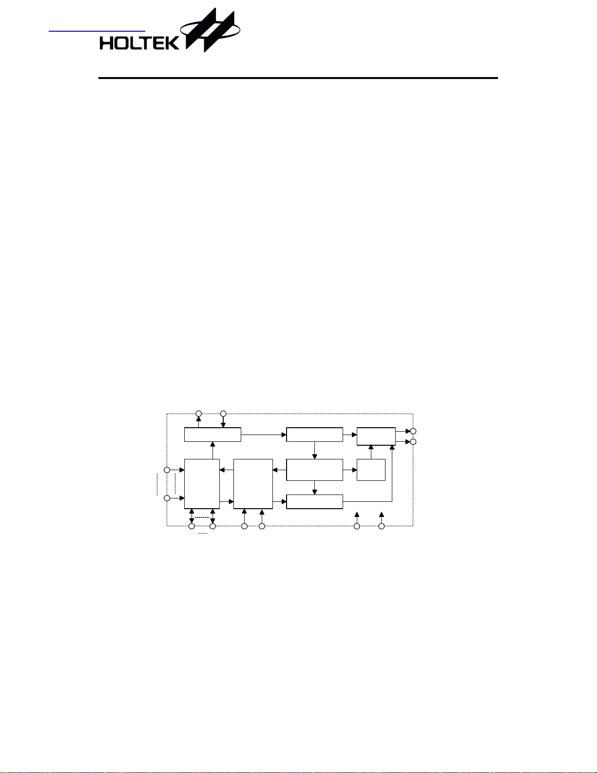
Block Diagram
R1
R8
X2 X1
O scillator D ivider
24 C ounter &
Keyboard
Matrix &
Gate
Circuit
C1 C8 AIN D7
Data ROM
& R egisters
¸
1 of 24 D ecoder
Binary D etector
1 March 2, 2000
D ata S elect
& Buffer
Sync.
Circuit
VDD VSS
DOUT
LED

Pin Assignment
Pad Assignment
R1
R2
R3
R4
DOUT
VDD
D7
X2
X1
VSS
20
1
19
2
18
3
17
4
16
5
15
6
14
7
13
8
12
9
11
10
H T6221
20 D IP/SOP
KI2
KI3
AIN
C1
C2
C3
C4
C5
C6
C7
C8
LED
KI1
HT6221/HT6222
1
R3
2
R4
3
R5
4
R6
5
R7
6
R8
VDD
D7
X2
X1
VSS
7
8
9
10
11
12
DOUT
24 D IP /S O P
KI0
H T6222
CCS
24
R2
23
R1
22
AIN
21
C1
20
C2
19
C3
18
C4
17
C5
16
C6
15
C7
14
C8
13
LED
KIO 0
19
KIO 1
18
KIO 2
17
16
KIO 3
15
KIO 4
14
KIO 5
KI4
KI5
KI6
KI7
REM
VDD
SEL
OSCO
23
24
1
2
3
4
5
6
7
8
21
22
9
10
OSCI
VSS
Chip size: 94 ´ 104 (mil)
20
(0 ,0 )
11
LM B
13
12
KIO 6
KIO 7
2
* The IC substrate should be connected to VDD in the PCB layout artwork.
2 March 2, 2000
HT6221/HT6222
Pad Coordinates Unit: mil
Pad No. X Y Pad No. X Y
1
2
3
4
5
6
7
8
9
10
11
12 24.31
-41.99
-41.99
-41.99
-41.99
-41.99 -5.61
-41.99 -28.31
-41.99 -37.83
-41.99 -46.88
-20.95 -46.88
-14.32 -46.88
-4.25 -46.88
Pin Description
HT6222
Pin No. Pin Name I/O
1~6 R3~R8 I
7 DOUT O CMOS OUT Serial data output pin, with a 38kHz carrier
8 VDD
9 D7 I CMOS IN Most significant data bit (D7) code setting
10 X2 O OSCILLATOR 455kHz resonator oscillator output
11 X1 I OSCILLATOR 455kHz resonator oscillator input
12 VSS
13 LED O CMOS OUT Transmission enable indicator output
14~21 C8~C1 I/O
22 AIN I
23~24 R1~R2 I
34.43 13 34.17
22.02 14 41.95
15.39 15 41.95
2.98 16 41.95
17 41.95 12.16
18 41.95 22.02
19 39.99 46.84
20 28.26 46.84
21
22
23
-46.88
Connection
¾¾
¾¾
CMOS IN/OUT
24
Internal
CMOS IN
Pull-low
Pull-low
CMOS IN
Pull-high
Pull-low
CMOS IN
Pull-low
-11.18
-23.16
-29.79
-39.27
Row control for keyboard matrix, active high
Positive power supply, 1.8V~3.5V for normal
operation
Negative power supply
Column control for keyboard matrix
Low byte address codes (8 bits) scan input
Row control for keyboard matrix, active high
-46.88
-30.26
-13.98
-4.12
46.84
46.84
46.84
46.84
Description
3 March 2, 2000
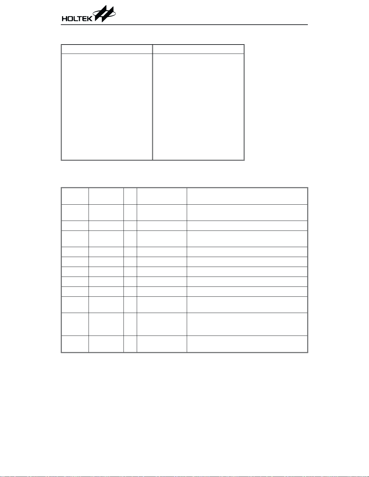
Approximate internal connection circuits
HT6221/HT6222
CMOS IN/O UT
V
DD
OSCILLATOR
X1
10M
W
CMOS IN/O UT
Pull-low
X2
EN
CMOS IN
Pull-low
CMOS IN
CMOS OUT
V
DD
Absolute Maximum Ratings
Supply Voltage.................................-0.3V to 6V
Input Voltage .................V
-0.3V to VDD+0.3V
SS
Note: These are stress ratings only. Stresses exceeding the range specified under "Absolute Maxi
mum Ratings" may cause substantial damage to the device. Functional operation of this device
at other conditions beyond those listed in the specification is not implied and prolonged exposure to extreme conditions may affect device reliability.
Storage Temperature.................-50°Cto125°C
Operating Temperature ..............-20°Cto75°C
-
Electrical Characteristic
Symbol Parameter
V
I
I
I
I
I
I
I
STB
DD
OH1
OL1
OH2
OL2
OH3
Operating Voltage
DD
Standby Current 3V Oscillator stops
Operating Current 3V
Output Source Current for DOUT 3V
Output Sink Current for DOUT 3V
Output Source Current for LED 3V
Output Sink Current for LED 3V
Output Source Current for C1~C8 3V
Ta=25°C
Test Conditions
Min. Typ. Max. Unit
V
4 March 2, 2000
Conditions
DD
¾¾
=455kHz
f
OSC
No load
V
=2.7V
O
V
=0.3V
O
V
=2.7V
O
V
=0.3V
O
V
=2.7V
O
1.8 3 3.5 V
0.1 1.0
¾
200 400
¾
-2.0 -4.0 ¾
50 100
mA
mA
mA
¾mA
-10 -60 ¾mA
1.2 2.0
-0.6 -2.0 ¾
¾
mA
mA

HT6221/HT6222
Symbol Parameter
I
V
V
V
V
V
V
R
R
R
R
f
OSC
OL3
Output Sink Current for C1~C8 3V
Input High Voltage for R1~R8 3V
IH1
Input Low Voltage for R1~R8 3V
IL1
Input High Voltage for C1~C8 3V
IH2
Input Low Voltage for C1~C8 3V
IL2
Input High Voltage for AIN 3V
IH3
Input Low Voltage for AIN 3V
IL3
Input Pull-high Resistance for AIN 3V
PH1
Input Pull-low Resistance for AIN 3V
PL1
Input Pull-low Resistance for R1~R8 3V
PL2
Input Pull-low Resistance for C1~C8 3V
PL3
System Frequency
Functional Description
Keyboard scan
The HT6221/HT6222 remain in the halt mode
during the standby state (at this time, the oscillator stops, and the standby current<1mA). The
HT6221 consists of 32 active keys, and the
HT6222 has 64 active keys. The keyboard
forms of the HT6221/ HT6222 are shown below.
·
The HT6221 keyboard form
C1 C2 C3 C4
K1
R1
R2
K2
R3
K3
R4
K4
K5
K6
K7
K8
K9
K10
K11
K12
C5 C6 C7 C8
K13
K17
K14
K18
K15
K19
K16
K20
K21
K22
K23
K24
K25
K26
K27
K28
K29
K30
K31
K32
Test Conditions
DD
Conditions
V
=0.3V
O
V
¾
¾
¾
¾
¾
¾
V
=0V
IN
V
=3V
IN
V
=3V
IN
V
=3V
IN
455kHz ceramic
¾
resonator
·
The HT6222 keyboard form
C1
C2 C3 C4 C5 C6 C7 C8
K9
K5
K1
R1
R2
R3
R4
R5
R6
R7
R8
K2
K3
K4
K33
K34
K35
K36
K6
K7
K8
K37
K38
K39
K40
K10
K11
K12
K41
K42
K43
K44
Min. Typ. Max. Unit
10 30
1.9
0
1.1
0
1.25
0
100 200 400
70 150 250
120 200 320
300 500 1500
455
¾
K17
K13
K18
K14
K19
K15
K20
K16
K49
K45
K50
K46
K51
K47
K52
K48
¾
¾
¾
¾
¾
¾
K21
K22
K23
K24
K53
K54
K55
K56
¾mA
3.0 V
0.8 V
3.0 V
0.6 V
3.0 V
0.6 V
kW
kW
kW
kW
kHz
¾
K25
K29
K26
K30
K27
K31
K28
K32
K57
K61
K58
K62
K59
K63
K60
K64
5 March 2, 2000

HT6221/HT6222
When one of the keys (32 or 64 keys) is triggered
for over 36ms, the oscillator is enabled and the
chip is activated. If the key is pressed and held
for 108ms or less, the 108ms transmission codes
are enabled and comprised of a header code
(9ms), an off code (4.5ms), low byte address
codes (9ms~18ms), high byte address codes
(9ms~18ms), 8-bit data codes (9ms~18ms), and
the inverse codes of the 8-bit data codes
(18ms~9ms). After the pressed key is held for
108ms, if the key is still held down, the trans
To avoid mistakes made by keyboard scanning
or simultaneous two-key inputs (except for the
three double-key active functions (K21+K22,
K21+K23, and K21+K24), the HT6221/HT6222
are facilitated with 36ms starting time.
The HT6221/HT6222 also provide three dou
ble-key active functions (K21+K22, K21+K23,
and K21+K24) for tape deck recording opera
tions. The double-key operation rules are
shown in timing 4 and timing 6.
-
mission codes turn out to be a composition of
header (9ms) and off codes (2.5ms) only.
Transmission codes
The transmission codes of the HT6221/6222 consist of a 9ms header code, a 4.5ms off code, 16-bit ad
dress codes (18ms~36ms), 9ms~18ms 8-bit data codes, and the inverse code of the 8-bit data codes. The
following is an illustration of the transmission codes:
Key-in
(K 1~K 64)
X2
DOUT
36m s m in.
Fosc=4 55kH z
4.5m s
9m s
45m s~63m s
(A 0~A15+D 0~D 7+D 0~D 7 )
108m s
Key Enables
9m s
38kH z,
33% duty carrier
2.5m s
108m s
0.56m s0.56m s
9m s
2.5m s
Output format for the DOUT
-
-
-
The output code carrier of the DOUT pin is shown in Timing 2:
38kHz
Carrier
8.77m s
26.3m s
38kHz carrier
The transmission codes employ the PPM (Pulse Position Modulation) method to represent their two
logic states by "0" (1.12ms) and "1" (2.24ms) as shown in Timing 3:
"Zero"
0.56m s
data period (1.12m s)
"O n e"
data period (2.24m s)
38kHz carrier
38kHz carrier
Logic states
6 March 2, 2000

HT6221/HT6222
·
Setting the address codes (A0~A15)
The algorithm rule of the address codes
(A0~A15) can be selected by mask option.
In this case, the 16-bit on-chip MASK ROM
(ROM1 and ROM2) are available, and the
value of ROM1 (8 bits) and ROM2 (8 bits) are
decided by one MASK LAYER. The current
value of ROM1 and ROM2 are both "00H".
The A0~A7 are set by logical OR between the
AIN
C1 C2 C3 C4 C5 C6 C7 C8
S8
(S w itc h O p e n : 0 , S w itc h C lo s e : 1 )
External S w itch S 0~S 15:
S9 S10 S11 S12 S13 S14 S15
1 0 0 0 1 1 0 0 1 0 1 0 0 1 0 0
H T6221/H T6222
external switch S0~S7 and the ROM1. The
A8~A15 equal some bits inverted to A0~A7,
the inversion are decided by Logical OR be
tween the external switch S8~S15 and the
ROM2.
For example:
The following is an illustration of these rules in
selecting the address codes (A0~A15).
200kW´8
1N 4148
S7S6S5S4S3S2S1S0
8
´
-
O n-chip R O M 1, R O M 2:
A0~A7:
A8'~A15':
A8~A15:
0 0 0 0 0 0 0 0 0 0 0 0 0 0 0 0
bit0 bit7 bit0 bit7
S0~S7 OR ROM1
1 0 0 0 1 1 0 0
S8~S15 O R RO M 2
1 0 1 0 0 1 0 0
A0 A1 A2 A3 A4 A5 A6 A7
1 1 0 1 0 1 1 1
Com plem ent
1 : n o n in v e rs io n
0: inversion
7 March 2, 2000

HT6221/HT6222
·
Values of the data codes (D0~D7)
The HT6221/HT6222 contain 32 and 64 ac
tive keys, respectively. Each key corresponds
to a data code. For tape deck recording, the
HT6221/HT6222 provide three double-key
functions. The double-key, single-key, and
double-key operation rules are shown in Ta
ble 3, Table 4, Timing 4, Timing 5 and Timing
6.
Table 4: K1~K64 single-key data code table
KEY
K1 0000 000 0/1 K33 0000 001 0/1
K2 1000 000 0/1 K34 1000 001 0/1
K3 0100 000 0/1 K35 0100 001 0/1
K4 1100 000 0/1 K36 1100 001 0/1
K5 0010 000 0/1 K37 0010 001 0/1
K6 1010 000 0/1 K38 1010 001 0/1
K7 0110 000 0/1 K39 0110 001 0/1
K8 1110 000 0/1 K40 1110 001 0/1
K9 0001 000 0/1 K41 0001 001 0/1
K10 1001 000 0/1 K42 1001 001 0/1
K11 0101 000 0/1 K43 0101 001 0/1
K12 1101 000 0/1 K44 1101 001 0/1
K13 0011 000 0/1 K45 0011 001 0/1
K14 1011 000 0/1 K46 1011 001 0/1
K15 0111 000 0/1 K47 0111 001 0/1
K16 1111 000 0/1 K48 1111 001 0/1
K17 0000 100 0/1 K49 0000 101 0/1
K18 1000 100 0/1 K50 1000 101 0/1
K19 0100 100 0/1 K51 0100 101 0/1
K20 1100 100 0/1 K52 1100 101 0/1
K21 0010 100 0/1 K53 0010 101 0/1
K22 1010 100 0/1 K54 1010 101 0/1
K23 0110 100 0/1 K55 0110 101 0/1
K24 1110 100 0/1 K56 1110 101 0/1
K25 0001 100 0/1 K57 0001 101 0/1
Data Codes
D0~D6
Data Code
D7
Table 3: Double-key data code table
-
-
KEY
K21+K22 1010110 0/1
K21+K23 0110110 0/1
K21+K24 1110110 0/1
Note: D7 is defined by an external switch
KEY
Data Codes
D0~D6
Data Codes
D0~D6
Data Code
D7
Data Code
D7
8 March 2, 2000

HT6221/HT6222
KEY
Data Codes
D0~D6
Data Code
D7
KEY
Data Codes
D0~D6
K26 1001 100 0/1 K58 1001 101 0/1
K27 0101 100 0/1 K59 0101 101 0/1
K28 1101 100 0/1 K60 1101 101 0/1
K29 0011 100 0/1 K61 0011 101 0/1
K30 1011 100 0/1 K62 1011 101 0/1
K31 0111 100 0/1 K63 0111 101 0/1
K32 1111 100 0/1 K64 1111 101 0/1
Note: D7 is defined by an external switch
D7=0 : connect to VDD
D7=1 : connect to VSS
K21 Input
Km Input
DOUT
K21 Input
36m s< t <126m s
36m s 108m s (m in.)
K21 code transm ission
K21
Km
36m s
(a )
K21
Data Code
D7
Km Input
DOUT
K21 Input
Km Input
DOUT
K21 Input
Km Input
DOUT
0< t <36m s
0< t <36m s
36m s< t <126m s
36m s
Km
N o transm ission
(b )
K21
Km
N o transm ission
(c )
K21
Km
36m s
108m s (m in.)
Km code transm ission
(d )
Invalid double-key input
9 March 2, 2000

HT6221/HT6222
(b)
Kn Input
DOUT
Kn Input
DOUT
K21 Input
K m In p u t
DOUT
36m s
36m s
36m s
Kn
t > 1 0 8 m s
Kn code transm ission
(a )
Kn
t <108m s
108m s
Kn code transm ission
Note: Kn can be one of K1~K64
Valid single-key input
K21
36m s
t > 1 2 6 m s
K21 code transm ission
Km
108m s (m in.)
K21+Km code
transm ission
Note: Km can be one of K22~K24
Valid double-key input
DOUT and LED
After the transmission codes are sent, the DOUT pin generates transmission codes with a carrier,
and the LED goes low to drive a transmission indicator.
10 March 2, 2000

Application Circuits
Application circuit 1
V
DD
HT6221/HT6222
1.8V~3.5V
51kW´8
330
W
100pF
X1 X2
7
D7
C1 C2 C3 C4 C5
1918171615141312123420
K1
K2
K3
K4
100pF
455kH z
ceram ic resonator
89
K5
K9
K6
K10
K7
K11
K8
K12
K13
K14
K15
K16
LED
11
LED
VDD
H T6221
C6 C7 C8 R1 R2 R3 R4
K29
K25
K21
K17
K30
K26
K22
K18
K31
K27
K23
K19
K32
K28
K24
K20
6
47mF/16V
1k
5
DOUT
VSS
AIN
In fra re d
47
W
W
8050
10
1N 4148´8
Note: Typical infrared diode: EL-1L2 (KODENSHI CORP.)
11 March 2, 2000

Application circuit 2
100pF
9
D7
11
X1 X2
100pF
455kH z
ceram ic resonator
10
V
DD
1.8V~3.5V
330
13
LED
H T6222
HT6221/HT6222
47mF/16V
W
1k
8
VDD
7
DOUT
In fra re d
47
W
W
8050
12
VSS
51kW´8
C1 C2 C3 C4 C5
2120191817161514232412345622
K9
K10
K11
K12
K41
K42
K43
K44
K13
K14
K15
K16
K45
K46
K47
K48
K1
K2
K3
K4
K33
K34
K35
K36
K5
K6
K7
K8
K37
K38
K39
K40
C6 C7 C8 R5 R6 R7 R8
K25
K21
K17
K26
K22
K18
K27
K23
K19
K28
K24
K20
K57
K53
K49
K58
K54
K50
K59
K55
K51
K60
K56
K52
R1 R2 R3 R4
K29
K30
K31
K32
K61
K62
K63
K64
1N 4148´8
AIN
Note: Typical infrared diode: EL-1L2 (KODENSHI CORP.)
12 March 2, 2000

HT6221/HT6222
Holtek Semiconductor Inc. (Headquarters)
No.3 Creation Rd. II, Science-based Industrial Park, Hsinchu, Taiwan, R.O.C.
Tel: 886-3-563-1999
Fax: 886-3-563-1189
Holtek Semiconductor Inc. (Taipei Office)
5F, No.576, Sec.7 Chung Hsiao E. Rd., Taipei, Taiwan, R.O.C.
Tel: 886-2-2782-9635
Fax: 886-2-2782-9636
Fax: 886-2-2782-7128 (International sales hotline)
Holtek Semiconductor (Hong Kong) Ltd.
RM.711, Tower 2, Cheung Sha Wan Plaza, 833 Cheung Sha Wan Rd., Kowloon, Hong Kong
Tel: 852-2-745-8288
Fax: 852-2-742-8657
Copyright Ó 2000 by HOLTEK SEMICONDUCTOR INC.
The information appearing in this Data Sheet is believed to be accurate at the time of publication. However, Holtek
assumes no responsibility arising from the use of the specifications described. Theapplications mentioned herein are
used solely for the purpose of illustration and Holtek makes no warranty or representation that such applications
will be suitable without further modification, nor recommends the use of its products for application that may pres
ent a risk to human life due to malfunction or otherwise. Holtek reserves the right to alter its products without prior
notification. For the most up-to-date information, please visit our web site at http://www.holtek.com.tw.
13 March 2, 2000
-
 Loading...