

Features
·
Operating voltage: 2.4V~12V
·
Low power and high noise immunity CMOS
technology
·
Low standby current
·
Minimum transmission word
-
Four words for TE trigger
-
One word for Data trigger
Applications
·
Burglar alarm system
·
Smoke and fire alarm system
·
Garage door controllers
·
Car door controllers
General Description
The 312encoders are a series of CMOS LSIs for remote
control system applications. They are capable of encod
ing 12 bits of information which consists of N address
bits and 12-N data bits. Each address/data input is externally trinary programmable if bonded out. They are
otherwise set floating internally. Various packages of
12
the 3
encoders offer flexible combinations of pro-
HT6010/HT6012/HT6014
312Series of Encoders
·
Built-in oscillator needs only 5% resistor
·
Easy interface with an RF or an infrared transmission
medium
·
Minimal external components
·
Pair with Holtek¢s312series of decoders
·
18-pin DIP, 20-pin SOP package
·
Car alarm system
·
Security system
·
Cordless telephones
·
Other remote control systems
grammable address/data which meet various appli
cations. The programmable address/data is transmitted
together with the header bits via an RF or an infrared
transmission medium upon receipt of a trigger signal. A TE
(HT6010) or a DATA (HT6012/HT6014) trigger can be
selected for application flexibility.
-
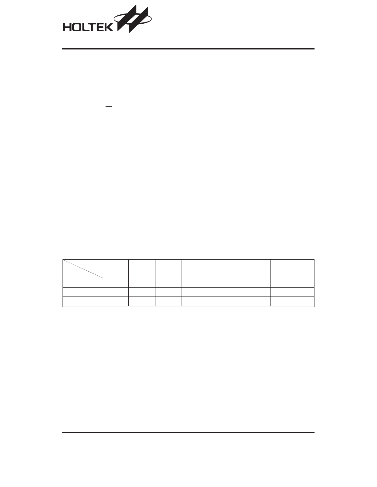
Selection Table
Function
Part No.
HT6010 8 4 0 RC oscillator TE
HT6012 10 0 2 RC oscillator D10~D11 Yes 18DIP, 20SOP
HT6014 8 0 4 RC oscillator D8~D11 Yes 18DIP, 20SOP
Note: Address/Data represents pins that can be either address or data according to the application requirement.
Address
No.
Address/
Data No.
Data
No.
Oscillator Trigger
LED
Indicator
No 18DIP, 20SOP
Package
Rev. 1.20 1 September 9, 2003
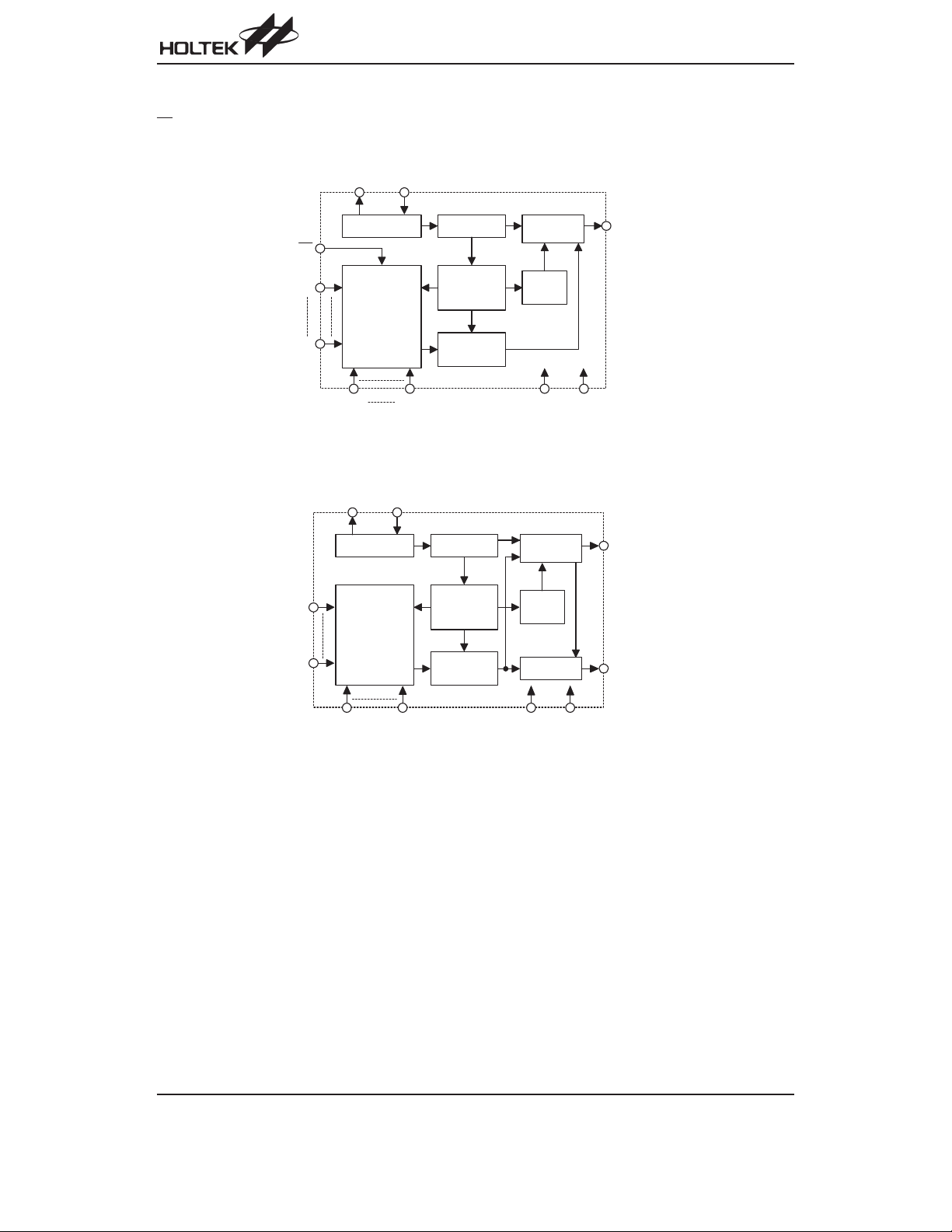
Block Diagram
TE Trigger
HT6010
O S C 2
HT6010/HT6012/HT6014
O S C 1
DATA Trigger
HT6012/HT6014
A d d r e s s
T E
A 0
A 7
O s c i l l a t o r
1 2
T r a n s m i s s i o n
G a t e C i r c u i t
A D 8 A D 1 1
O S C 2
O S C 1
O s c i l l a t o r
1 2
T r a n s m i s s i o n
G a t e C i r c u i t
3 D i v i d e r
¸
1 2 C o u n t e r
¸
a n d 1 o f 1 2
D e c o d e r s
T r i n a r y
D e t e c t o r
3 D i v i d e r
¸
1 2 C o u n t e r
¸
a n d 1 o f 1 2
D e c o d e r s
T r i n a r y
D e t e c t o r
D a t a S e l e c t
a n d B u f f e r
S y n c .
C i r c u i t
V D D V S S
D a t a S e l e c t
a n d B u f f e r
S y n c .
C i r c u i t
L E D C i r c u i t
D O U T
D O U T
L E D
D a t a
V D D V S S
Note: The address/data pins are available in various combinations (refer to the address/data table).
Rev. 1.20 2 September 9, 2003
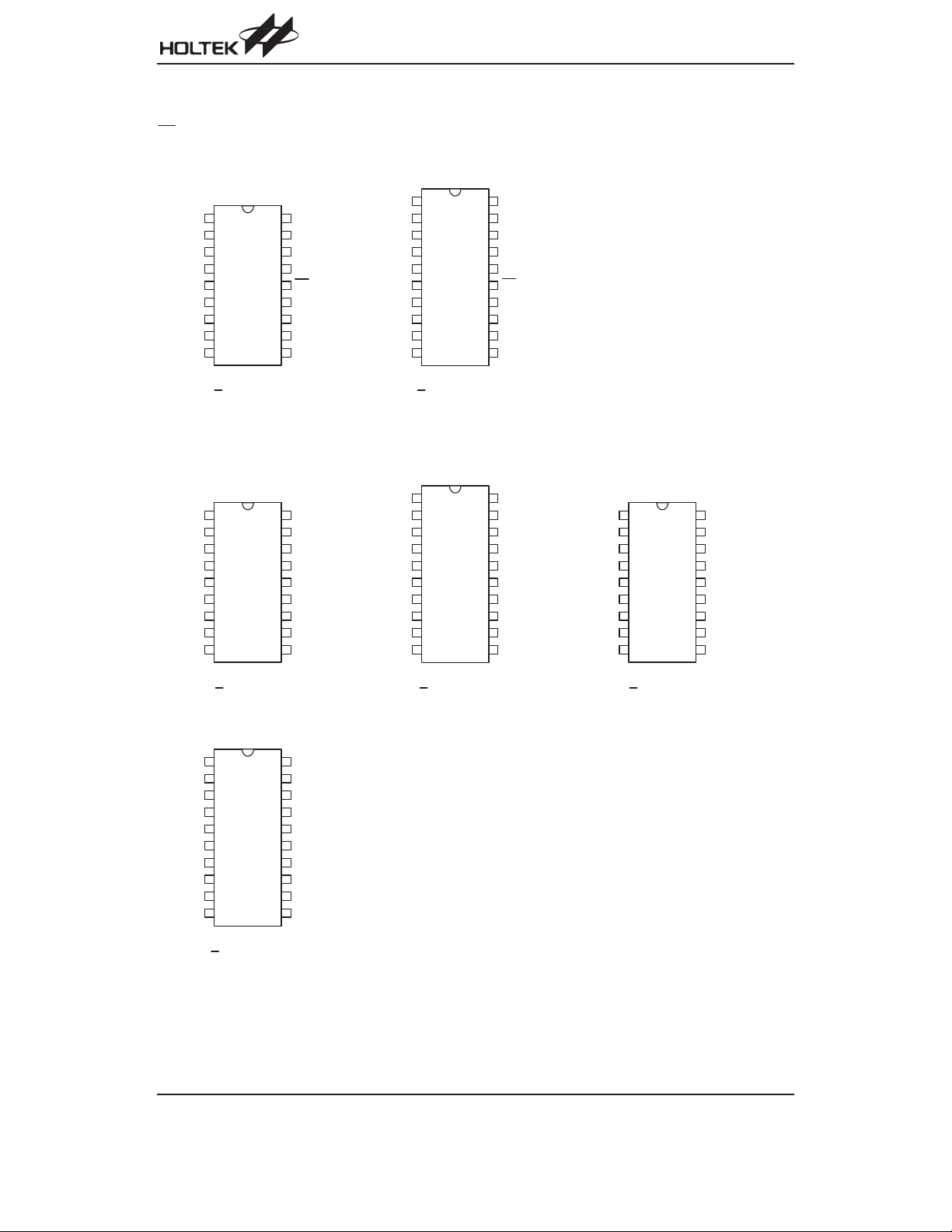
Pin Assignment
T E T r i g g e r T y p e
HT6010/HT6012/HT6014
8 - A d d r e s s
4 - A d d r e s s / D a t a
A 0
A 1
A 2
A 3
A 4
A 5
A 6
A 7
V S S
1 8
1
1 7
2
1 6
3
1 5
4
1 4
5
1 3
6
1 2
7
1 1
8
1 0
9
H T 6 0 1 0
1 8 D I P - A
D A T A T r i g g e r T y p e
1 0 - A d d r e s s
2 - D a t a
1
A 0
2
A 1
3
A 2
4
A 3
5
A 4
6
A 5
7
A 6
8
A 7
9
V S S
H T 6 0 1 2
1 8 D I P - A
8 - A d d r e s s
4 - A d d r e s s / D a t a
N C
2 0
V D D
1 9
D O U T
1 8
O S C 2
1 7
O S C 1
1 6
T E
1 5
A D 1 1
1 4
A D 1 0
1 3
A D 9
1 2
A D 8
1 1
V D D
D O U T
O S C 2
O S C 1
T E
A D 1 1
A D 1 0
A D 9
A D 8
V S S
N C
1
A 0
2
A 1
3
A 2
4
A 3
5
A 4
6
A 5
7
A 6
8
A 7
9
1 0
H T 6 0 1 0
2 0 S O P - A
1 0 - A d d r e s s
2 - D a t a
N C
1 8
V D D
1 7
D O U T
1 6
O S C 2
1 5
O S C 1
1 4
L E D
1 3
D 1 1
1 2
D 1 0
1 1
A 9
1 0
A 8
A 0
A 1
A 2
A 3
A 4
A 5
A 6
A 7
V S S
2 0
1
2
3
4
5
6
7
8
9
1 0
N C
1 9
V D D
1 8
D O U T
1 7
O S C 2
1 6
O S C 1
1 5
L E D
1 4
D 1 1
1 3
D 1 0
1 2
A 9
1 1
A 8
H T 6 0 1 2
2 0 S O P - A
8 - A d d r e s s
4 - D a t a
A 0
A 1
A 2
A 3
A 4
A 5
A 6
A 7
V S S
1 8 D I P - A
1
2
3
4
5
6
7
8
9
H T 6 0 1 4
1 8
V D D
1 7
D O U T
1 6
O S C 2
1 5
O S C 1
1 4
L E D
1 3
D 1 1
1 2
D 1 0
1 1
D 9
1 0
D 8
8 - A d d r e s s
4 - D a t a
V S S
N C
1
A 0
2
A 1
3
A 2
4
A 3
5
A 4
6
A 5
7
A 6
8
A 7
9
1 0
N C
2 0
V D D
1 9
D O U T
1 8
O S C 2
1 7
O S C 1
1 6
L E D
1 5
D 1 1
1 4
D 1 0
1 3
D 9
1 2
D 8
1 1
H T 6 0 1 4
2 0 S O P - A
Rev. 1.20 3 September 9, 2003
HT6010/HT6012/HT6014
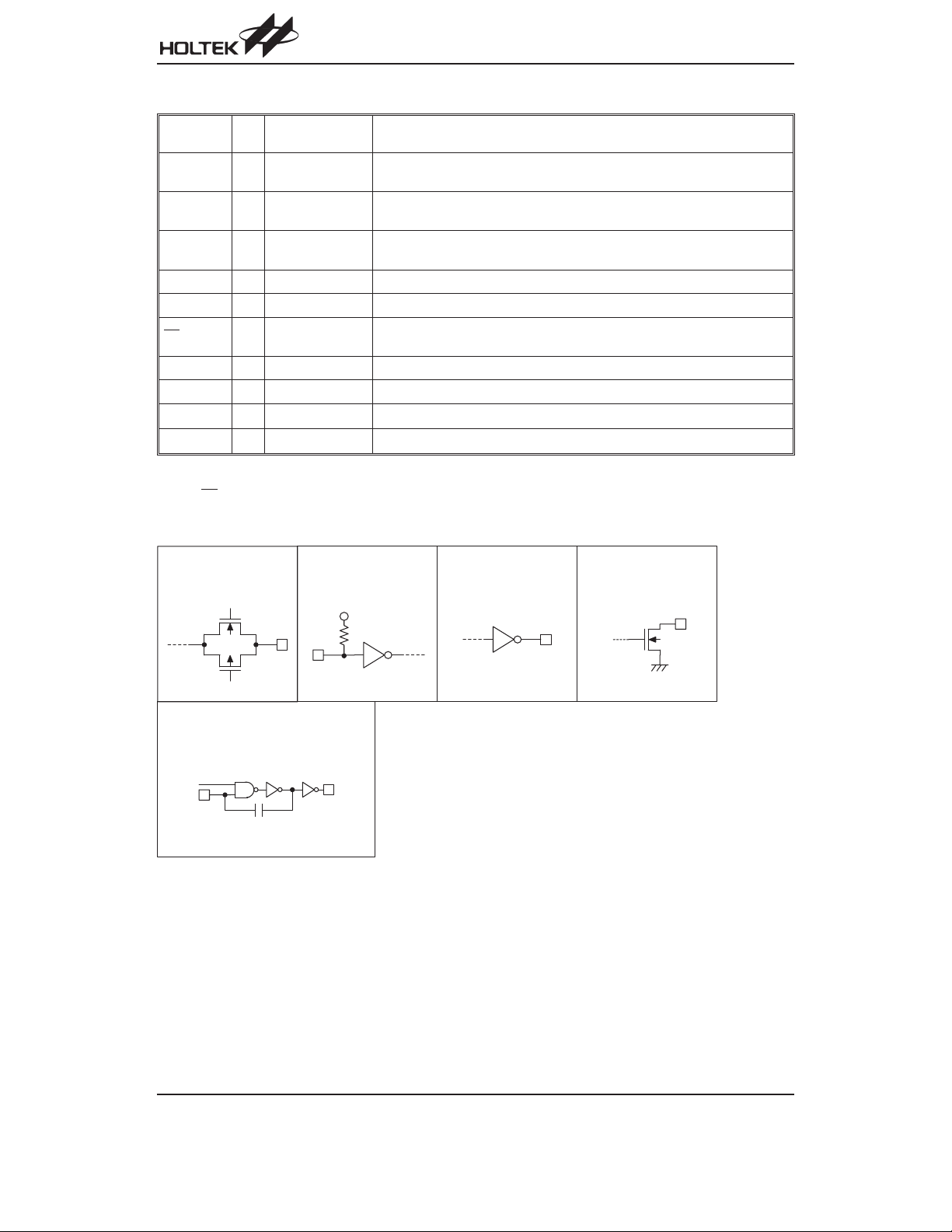
Pin Description
Pin Name I/O
A0~A9 I
AD8~AD11 I
D8~D11 I
DOUT O CMOS OUT Encoder data serial transmission output
LED O NMOS OUT Transmission enable indicator, active low
TE
OSC1 I OSCILLATOR Oscillator input pin
OSC2 O OSCILLATOR Oscillator output pin
VSS
VDD
Note: D8~D11 are data input and transmission enable pins of the HT6012/HT6014.
I
¾¾
¾¾
is the transmission enable pin of the HT6010.
TE
Internal
Connection
TRANSMISSION
GATE
TRANSMISSION
GATE
CMOS IN
Pull-high
CMOS IN
Pull-high
Description
Input pins for address A0~A9 setting
They can be externally set to VDD or VSS or left open.
Input pins for address/data (AD8~AD11) setting
They can be externally set to VDD or VSS or left open.
Input pins for data (D8~D11) setting and transmission enable (active low)
They can be externally set to VSS or left open (see Note).
Transmission enable, active low (see Note)
Negative power supply, ground
Positive power supply
Approximate Internal Connections
T R A N S M I S S I O N
G A T E
C M O S I N
P u l l - h i g h
O S C I L L A T O R
O S C 1
E N
O S C 2
Absolute Maximum Ratings
Supply Voltage............................VSS-0.3V to VSS+13V
Input Voltage ................................V
-0.3 to VDD+0.3V
SS
C M O S O U T N M O S O U T
Storage Temperature ............................-50°Cto125°C
Operating Temperature...........................-20°Cto75°C
Note: These are stress ratings only. Stresses exceeding the range specified under ²Absolute Maximum Ratings² may
cause substantial damage to the device. Functional operation of this device at other conditions beyond those
listed in the specification is not implied and prolonged exposure to extreme conditions may affect device reliabil
ity.
Rev. 1.20 4 September 9, 2003
-

HT6010/HT6012/HT6014
Electrical Characteristics
Symbol Parameter
V
DD
I
STB
I
DD
I
LED
I
DOUT
V
IH
V
IL
f
OSC
R
TE
R
DATA
Operating Voltage
Standby Current
Operating Current
LED Sink Current 5V
Output Drive Current
²H² Input Voltage ¾¾
²L² Input Voltage ¾¾
Oscillator Frequency 5V
TE Pull-high Resistance 5V
D8~D11 Pull-high Resistance 5V
Test Conditions
V
DD
Conditions
¾¾
3V
Oscillator stops
12V
3V
12V
5V
5V
No load, f
=0.5V
V
LED
=0.9VDD(Source)
V
OH
V
=0.1VDD(Sink)
OL
R
OSC
=0V
V
TE
V
DATA
=3kHz
OSC
=1MW¾3¾
=0V
Min. Typ. Max. Unit
2.4 5 12 V
¾
¾
¾
¾
0.1 1
24
250 500
600 1200
1.5 3
-0.6 -1.2 ¾
0.6 1.2
0.8V
0
¾
¾
DD
¾
¾
1.5 3
1.5 3
Functional Description
Operation
12
The 3
series of encoders begin with a four (HT6010) or a one (HT6012/HT6014) word transmission cycle upon receipt
of a transmission enable (TE
as long as the transmission enable (TE
output completes its final cycle and then stops as shown below.
for the HT6010 or D8~D11 for the HT6012/HT6014, active low). This cycle will repeat itself
or D8~D11) is held low. Once the transmission enable returns high the encoder
¾
¾
V
0.2V
DD
DD
Ta=25°C
mA
mA
mA
mA
mA
mA
mA
V
V
kHz
MW
MW
T E o r
D 8 ~ D 1 1
< 1 w o r d
E n c o d e r
D a t a O u t
1 o r 4 w o r d s
T r a n s m i t t e d
C o n t i n u o u s l y
1 o r 4
w o r d s
Transmission Timing
Information Word
An information word is composed of four periods as shown:
1 / 6 b i t s y n c . p e r i o d
p i l o t p e r i o d ( 6 b i t s )
a d d r e s s c o d e p e r i o d
d a t a c o d e
p e r i o d
Composition of Information
Rev. 1.20 5 September 9, 2003

HT6010/HT6012/HT6014
Address/Data Waveform
Each programmable address/data pin can be externally set to one of the following three logic states:
f
O S C
" O n e "
" Z e r o "
" O p e n "
A d d r e s s / D a t a B i t
Address/Data Bit Waveform
The ²Open² state data input is interpreted as logic high by the decoder since its output has only two states.
Address/Data Programming (Preset)
The status of each address/data pin can be individually preset to a logic ²high², ²low²,or²floating². If a transmission en
able signal is applied, the encoder scans and transmits the status of the 12 bits of address/data serially in the order A0
to AD11 for the HT6010 and A0 to D11 for the HT6012/HT6014.
If the trigger signal is not applied, the chip only consumes a standby current which is less than 1mA (for V
The address pins are usually preset so as to transmitdata codes with their own particular security codes by the DIP switches
or PCB wiring, while data is selected using push button or electronic switches.
DD
=5V).
-
Address/Data Sequence
The following table provides the position of the address/data sequence for various modelsof the 3
Part No.
01234567891011
Address/Data Bits
12
series encoders.
HT6010 A0 A1 A2 A3 A4 A5 A6 A7 AD8 AD9 AD10 AD11
HT6012 A0 A1 A2 A3 A4 A5 A6 A7 A8 A9 D10 D11
HT6014 A0 A1 A2 A3 A4 A5 A6 A7 D8 D9 D10 D11
Transmission Enable
For the TE
trigger type of encoders, transmission is enabled by applying a low signal to the TE pin. But for the Data trig
ger type, it is enabled by applying a low signal to one of the data pins D8~D11.
-
Rev. 1.20 6 September 9, 2003

Flowchart
HT6010/HT6012/HT6014
P o w e r o n
S t a n d b y m o d e
N o
T r a n s m i s s i o n
e n a b l e d ?
Y e s
C o d e w o r d
t r a n s m i t t e d
c o n t i n u o u s l y
N o
T r a n s m i s s i o n
s t i l l e n a b l e d ?
Y e s
C o d e w o r d
t r a n s m i t t e d
c o n t i n u o u s l y
Note: D8~D11 are transmission enable of the HT6012/HT6014.
is the transmission enable of the HT6010.
TE
Oscillator Frequency vs. Supply Voltage
O S C
f
( S c a l e )
7 . 0 0
6 . 0 0
R
4 7 0 k
5 1 0 k
5 6 0 k
O S C
(W)
5 . 0 0
4 . 0 0
( 3 k H z ) 3 . 0 0
2 . 0 0
1 . 0 0
2 3 4
5 6 7 8 9 1 0 1 1 1 2 1 3
The recommended oscillator frequency is f
(decoder) @ 33 f
OSCD
OSCE
6 2 0 k
6 8 0 k
7 5 0 k
8 2 0 k
9 1 0 k
1 . 0 M
1 . 2 M
1 . 5 M
2 . 0 M
D D
V
(encoder)
( V D C )
Rev. 1.20 7 September 9, 2003

Application Circuits
HT6010/HT6012/HT6014
T r a n s m i t t e r C i r c u i t
1
A 0
2
A 1
3
A 2
4
A 3
5
A 4
6
A 5
7
A 6
8
A 7
9
V S S
V D D
D O U T
O S C 2
O S C 1
A D 1 1
A D 1 0
A D 9
A D 8
H T 6 0 1 0
T r a n s m i t t e r C i r c u i t
1
A 0
2
A 1
3
A 2
4
A 3
5
A 4
6
A 5
7
A 6
8
A 7
9
V S S
V D D
D O U T
O S C 2
O S C 1
L E D
D 1 1
D 1 0
V
D D
1 8
1 7
1 6
R
O S C
1 5
1 4
T E
1 3
1 2
1 1
1 0
T r a n s m i t t e r C i r c u i t
1
A 0
2
A 1
3
A 2
4
A 3
5
A 4
6
A 5
7
A 6
8
A 7
9
V S S
V D D
D O U T
O S C 2
O S C 1
L E D
D 1 1
D 1 0
V
D D
1 8
1 7
1 6
R
O S C
1 5
1 4
1 3
1 2
1 1
A 9
1 0
A 8
R
H T 6 0 1 2
V
D D
1 8
1 7
1 6
R
O S C
1 5
1 4
1 3
1 2
1 1
D 9
1 0
D 8
R
H T 6 0 1 4
Rev. 1.20 8 September 9, 2003
Package Information
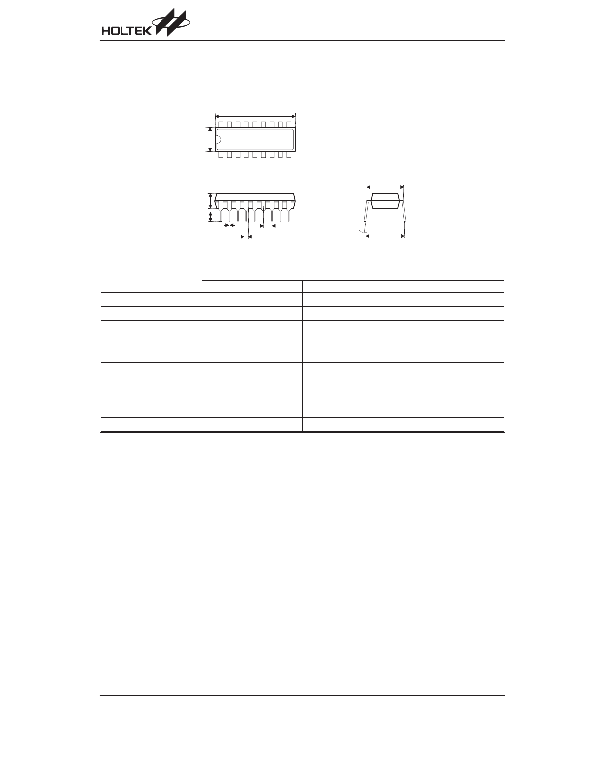
18-pin DIP (300mil) Outline Dimensions
HT6010/HT6012/HT6014
A
1 8
B
1
C
D
E
F
Symbol
Min. Nom. Max.
A 895
B 240
C 125
D 125
E16
F50
G
¾
H 295
I 335
1 0
9
H
a
G
I
Dimensions in mil
¾
¾
¾
¾
¾
¾
100
¾
¾
a 0°¾15°
915
260
135
145
20
70
¾
315
375
Rev. 1.20 9 September 9, 2003

20-pin SOP (300mil) Outline Dimensions
HT6010/HT6012/HT6014
2 0
A
1
C
C '
D
E F
Symbol
A 394
B 290
C14
C¢
D92
E
F4
G32
H4
1 1
B
1 0
G
H
a
Dimensions in mil
Min. Nom. Max.
¾
¾
¾
490
¾
¾
¾
50
¾¾
¾
¾
a 0°¾10°
419
300
20
510
104
¾
38
12
Rev. 1.20 10 September 9, 2003

Product Tape and Reel Specifications
Reel Dimensions
HT6010/HT6012/HT6014
T 2
A
B
T 1
D
SOP 20W
Symbol Description Dimensions in mm
A Reel Outer Diameter
B Reel Inner Diameter
C Spindle Hole Diameter
D Key Slit Width
T1 Space Between Flange
T2 Reel Thickness
330±1.0
62±1.5
13.0+0.5
2.0±0.5
24.8+0.3
30.2±0.2
C
-0.2
-0.2
Rev. 1.20 11 September 9, 2003

Carrier Tape Dimensions
HT6010/HT6012/HT6014
D
E
F
PD 1
P 1P 0
W
A 0
B 0
C
SOP 20W
Symbol Description Dimensions in mm
W Carrier Tape Width
P Cavity Pitch
E Perforation Position
F Cavity to Perforation (Width Direction)
24.0+0.3
12.0±0.1
1.75±0.1
11.5±0.1
D Perforation Diameter 1.5+0.1
D1 Cavity Hole Diameter 1.5+0.25
P0 Perforation Pitch
P1 Cavity to Perforation (Length Direction)
A0 Cavity Length
B0 Cavity Width
K0 Cavity Depth
t Carrier Tape Thickness
4.0±0.1
2.0±0.1
10.8±0.1
13.3±0.1
3.2±0.1
0.3±0.05
C Cover Tape Width 21.3
t
K 0
-0.1
Rev. 1.20 12 September 9, 2003

Holtek Semiconductor Inc. (Headquarters)
No.3, Creation Rd. II, Science Park, Hsinchu, Taiwan
Tel: 886-3-563-1999
Fax: 886-3-563-1189
http://www.holtek.com.tw
Holtek Semiconductor Inc. (Taipei Sales Office)
4F-2, No. 3-2, YuanQu St., Nankang Software Park, Taipei 115, Taiwan
Tel: 886-2-2655-7070
Fax: 886-2-2655-7373
Fax: 886-2-2655-7383 (International sales hotline)
HT6010/HT6012/HT6014
Holtek Semiconductor Inc. (Shanghai Sales Office)
7th Floor, Building 2, No.889, Yi Shan Rd., Shanghai, China 200233
Tel: 021-6485-5560
Fax: 021-6485-0313
http://www.holtek.com.cn
Holtek Semiconductor Inc. (Shenzhen Sales Office)
5/F, Unit A, Productivity Building, Cross of Science M 3rd Road and Gaoxin M 2nd Road, Science Park, Nanshan District,
Shenzhen, China 518057
Tel: 0755-8616-9908, 8616-9308
Fax: 0755-8616-9533
Holtek Semiconductor Inc. (Beijing Sales Office)
Suite 1721, Jinyu Tower, A129 West Xuan Wu Men Street, Xicheng District, Beijing, China 100031
Tel: 010-6641-0030, 6641-7751, 6641-7752
Fax: 010-6641-0125
Holtek Semiconductor Inc. (Chengdu Sales Office)
709, Building 3, Champagne Plaza, No.97 Dongda Street, Chengdu, Sichuan, China 610016
Tel: 028-6653-6590
Fax: 028-6653-6591
Holmate Semiconductor, Inc. (North America Sales Office)
46729 Fremont Blvd., Fremont, CA 94538
Tel: 510-252-9880
Fax: 510-252-9885
http://www.holmate.com
Copyright Ó 2003 by HOLTEK SEMICONDUCTOR INC.
The information appearing in this Data Sheet is believed to be accurate at the time of publication. However, Holtek as
sumes no responsibility arising from the use of the specifications described. The applications mentioned herein are used
solely for the purpose of illustration and Holtek makes no warranty or representation that such applications will be suitable
without further modification, nor recommends the use of its products for application that may present a risk to human life
due to malfunction or otherwise. Holtek¢s products are not authorized for use as critical components in life support devices
or systems. Holtek reserves the right to alter its products without prior notification. For the most up-to-date information,
please visit our web site at http://www.holtek.com.tw.
-
Rev. 1.20 13 September 9, 2003
 Loading...