


查询HT48R06A-1供应商
HT48R06A-1
Preliminary
8-Bit OTP Microcontroller
Features
Operating voltage:
·
f
=4MHz: 3.3V~5.5V
SYS
f
=8MHz: 4.5V~5.5V
SYS
13 bidirectional I/O lines
·
An interrupt input shared with an I/O line
·
8-bit programmable timer/event counter with
·
overflow interrupt and 8-stage prescaler
On-chip crystal and RC oscillator
·
Watchdog timer
·
1024´14 program memory PROM
·
64´8 data memory RAM
·
Buzzer driving pair and PFD supported
·
General Description
The device is an 8-bit high performance
RISC-like microcontroller designed for multi
ple I/O product applications. The device is par
ticularly suitable for use in products such as
remote controllers, fan/light controllers, wash
ing machine controllers, scales, toys and vari-
Halt function and wake-up feature reduce
·
power consumption
Up to 0.5ms instruction cycle with 8MHz
·
system clock at V
Allinstructionsinoneortwomachinecycles
·
14-bit table read instruction
·
Two-level subroutine nesting
·
Bit manipulation instruction
·
63 powerful instructions
·
Low voltage reset function
·
18-pin DIP/SOP package
·
ous subsystem controllers. A halt feature is
included to reduce power consumption.
-
The program and option memories can be elec
trically programmed, making the microcontrol
ler suitable for use in product development.
DD
=5V
-
-
1 February 25, 2000
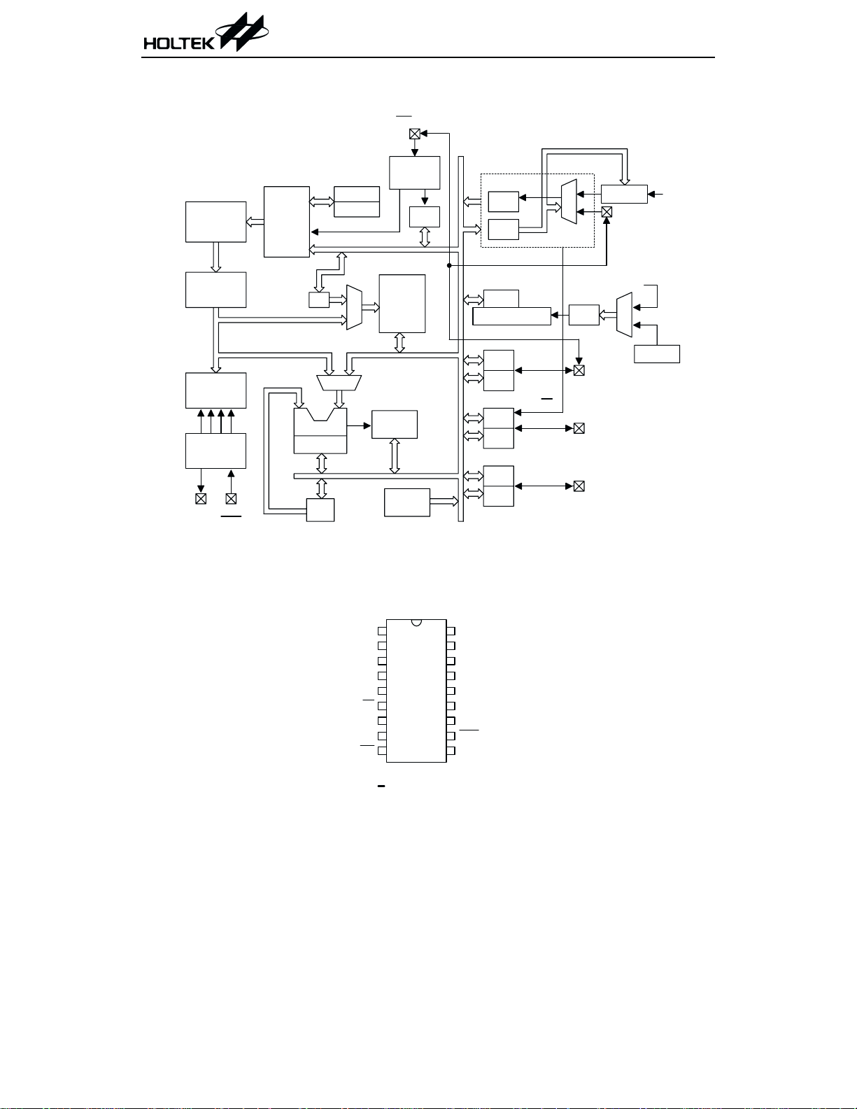
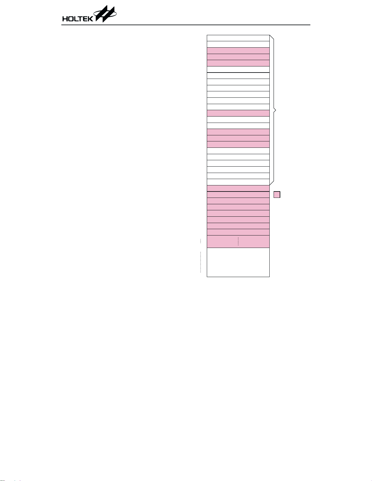
Block Diagram
Program
ROM
Program
C ounter
Preliminary
IN T /P C 0
Interrupt
Circuit
STACK0
STACK1
IN T C
TM R
TM RC
HT48R06A-1
M
P resca ler
U
X
TM R/PC1
f
SYS
Instruction
R egister
Instruction
D ecoder
Tim ing
G enerator
OSC2 OSC1
RES
VDD
VSS
Pin Assignment
MP
MUX
ALU
Shifter
ACC
M
U
X
PA3
PA2
PA1
PA0
PB2
PB1/BZ
PB0/BZ
VSS
PC0/INT
PC0
DATA
Memory
STATUS
Option
PRO M
18
1
17
2
16
3
15
4
14
5
13
6
12
7
11
8
10
9
H T 48R 06A -1
1 8 D IP /S O P
WDTS
W D T P rescaler
PCC
PC
PBC
PB
PAC
PA
PA4
PA5
PA6
PA7
OSC2
OSC1
VDD
RES
PC1/TMR
PORT C
BZ/BZ
PORT B
PORT A
SYS CLK/4
WDT
PC0~PC 1
PB0~PB2
PA0~PA7
PC1
M
U
X
RC OSC
2 February 25, 2000
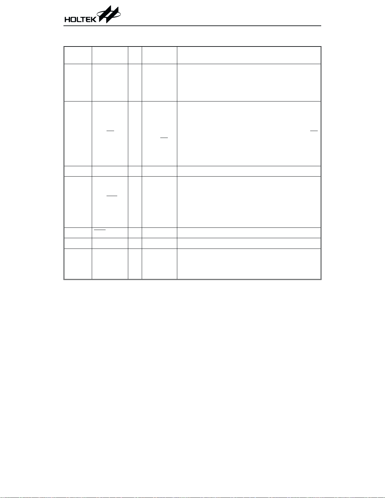
Pin Description
Preliminary
HT48R06A-1
Pin No. Pin Name I/O
4~1
18~15
7
6
5
8 VSS
9
10
11 RES
12 VDD
13
14
PA0~PA7 I/O
PB0/BZ
PB1/BZ
PB2
PC0/INT
PC1/TMR
OSC1
OSC2
I/O
¾¾
I/O Pull-high*
¾¾
ROM Code
Pull-high*
Wake-up
Pull-high*
I
I
O
Option
I/O or
BZ/BZ
¾
Crystal
or RC
Description
Bidirectional 8-bit input/output port. Each bit can be
configured as wake-up input by ROM code option.
Software instructions determine the CMOS output or
schmitt trigger input with a pull-high resistor (deter
mined by pull-high options).
Bidirectional 3-bit input/output port. Software in
structions determine the CMOS output or schmitt
trigger input with a pull-high resistor (determined by
pull-high options).
The PB0 and PB1 are pin-shared with the BZ and BZ
respectively. Once the PB0 and PB1 are selected as
buzzer driving outputs, the output signals come from
an internal PFD generator (shared with timer/event
counter).
Negative power supply, ground
Bidirectional I/O lines. Software instructions deter
mine the CMOS output or SCHMITT trigger input
with a pull-high resistor (determined by pull-high op
tions). The external interrupt and timer input are
pin-shared with the PC0 and PC1, respectively. The
external interrupt input is activated on a high to low
transition.
Schmitt trigger reset input. Active low
Positive power supply
OSC1, OSC2 are connected to an RC network or Crystal (determined by ROM code option) for the internal
system clock. In the case of RC operation, OSC2 is the
output terminal for 1/4 system clock.
-
-
,
-
-
* All pull-high resistors are controlled by an option bit.
Absolute Maximum Ratings
Supply Voltage ...............VSS-0.3V to VSS+5.5V
Input Voltage.................V
Note: These are stress ratings only. Stresses exceeding the range specified under "Absolute Maxi
mum Ratings" may cause substantial damage to the device. Functional operation of this device
at other conditions beyond those listed in the specification is not implied and prolonged expo
sure to extreme conditions may affect device reliability.
-0.3V to VDD+0.3V
SS
Storage Temperature.................-50°Cto125°C
Operating Temperature ..............-40°Cto85°C
3 February 25, 2000
-
-
Preliminary
HT48R06A-1
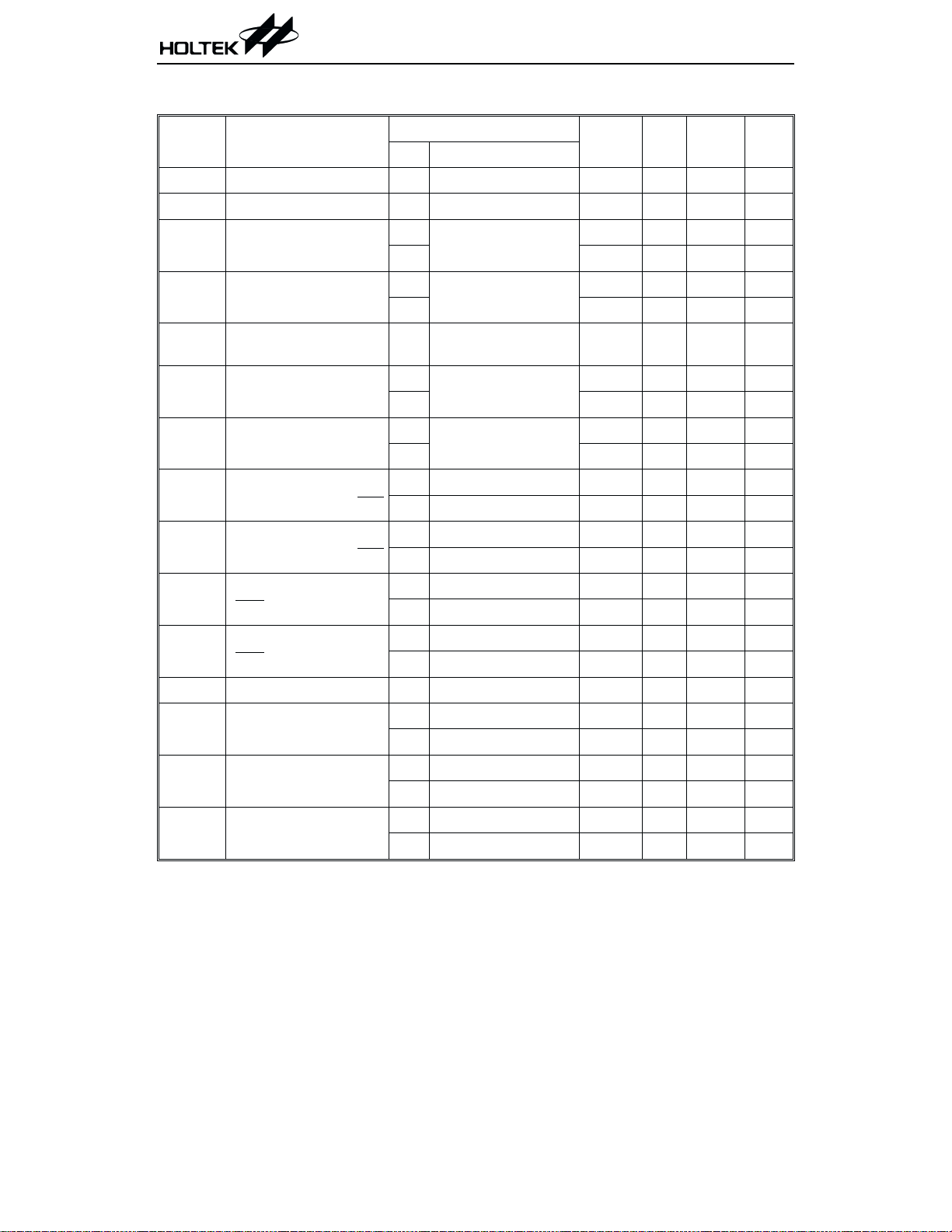
D.C. Characteristics
Symbol Parameter
V
V
I
DD1
I
DD2
I
DD3
I
STB1
I
STB2
V
V
V
V
V
I
OL
I
OH
R
DD1
DD2
IL1
IH1
IL3
IH3
LVR
PH
Operating Voltage
Operating Voltage
Operating Current
(Crystal OSC)
Operating Current
(RC OSC)
Operating Current
(Crystal OSC)
Standby Current
(WDT Enabled)
Standby Current
(WDT Disabled)
Input Low Voltage for
I/O Ports, TMR and INT
Input High Voltage for
I/O Ports, TMR and INT
Input Low Voltage
(RES
)
Input High Voltage
(RES
)
Low Voltage Reset
I/O Port Sink Current
I/O Port Source
Current
Pull-high Resistance
Test Conditions
V
DD
¾
¾
3.3V
5V
3.3V
5V
Conditions
=4MHz
f
SYS
=8MHz
f
SYS
No load, f
No load, f
SYS
SYS
=4MHz
=4MHz
5V No load, fsys=8MHz
3.3V
No load, system Halt
5V
3.3V
No load, system Halt
5V
3.3V
5V
3.3V
5V
3.3V
5V
3.3V
5V
¾
¾
¾
¾
¾
¾
¾
¾
¾¾
V
3.3V
5V
3.3V
5V
3.3V
5V
=0.1V
OL
V
OL
V
OH
V
OH
=0.1V
=0.9V
=0.9V
DD
DD
DD
DD
¾
¾
Ta=25°C
Min. Typ. Max. Unit
3.3
4.5
¾
¾
¾
¾
¾
¾
¾
¾¾
¾¾
¾¾
¾¾
0
0
0.8V
0.8V
0
0
0.9V
0.9V
DD
DD
DD
DD
¾
¾
¾
¾
¾
¾
¾
¾
5.5 V
5.5 V
12mA
24mA
12mA
24mA
510mA
5
10
1
2
0.2V
DD
0.2V
DD
V
DD
V
DD
0.4V
DD
0.4V
DD
V
DD
V
DD
3.1 3.2 3.3 V
48
10 20
¾
¾
-2 -4 ¾
-5 -10 ¾
mA
mA
mA
mA
40 60 80
10 30 50
mA
mA
mA
mA
V
V
V
V
V
V
V
V
kW
kW
4 February 25, 2000

Preliminary
HT48R06A-1
A.C. Characteristics
Symbol Parameter
f
SYS1
f
SYS2
f
TIMER
t
WDTOSC
t
WDT1
t
WDT2
t
RES
t
SST
t
INT
System Clock
(Crystal OSC)
System Clock (RC OSC)
Timer I/P Frequency (TMR)
Watchdog Oscillator
Watchdog Time-out Period
(RC)
Watchdog Time-out Period
(System Clock)
External Reset Low Pulse
Width
System Start-up Timer
Period
Interrupt Pulse Width
Ta=25°C
Test Conditions
Min. Typ. Max. Unit
V
DD
3.3V
5V
3.3V
5V
3.3V
5V
3.3V
5V
3.3V
5V 9 17 35 ms
¾
¾¾
¾
¾¾
Conditions
¾
¾
¾
¾
¾
¾
¾
¾
Without WDT
prescaler
Without WDT
prescaler
Power-up, reset or
wake-up from Halt
400
400
400
400
0
0
¾
¾
¾
¾
¾
¾
4000 kHz
8000 kHz
4000 kHz
4000 kHz
4000 kHz
4000 kHz
43 86 168
35 65 130
11 22 43 ms
1024
¾
¾
1
¾¾ms
1024
1
¾¾ms
¾
¾
t
t
ms
ms
SYS
SYS
5 February 25, 2000
Preliminary
Functional Description
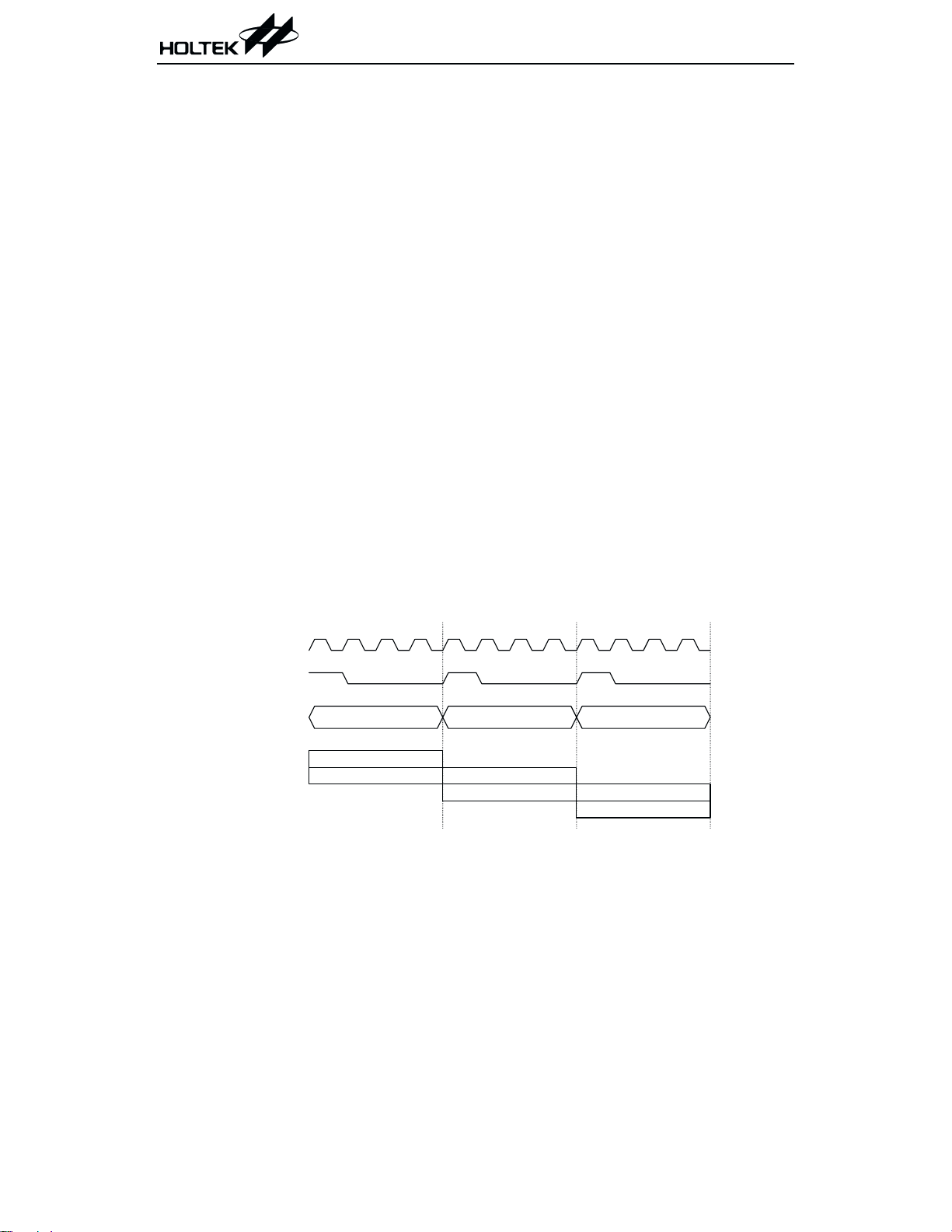
Execution flow
The system clock for the microcontroller is de
rived from either a crystal or an RC oscillator.
The system clock is internally divided into four
non-overlapping clocks. One instruction cycle
consists of four system clock cycles.
Instruction fetching and execution are
pipelined in such a way that a fetch takes an in
struction cycle while decoding and execution
takes the next instruction cycle. However, the
pipelining scheme causes each instruction to ef
fectively execute in a cycle. If an instruction
changes the program counter, two cycles are re
quired to complete the instruction.
Program counter - PC
The program counter (PC) controls the se
quence in which the instructions stored in pro
gram PROM are executed and its contents
specify full range of program memory.
After accessing a program memory word to fetch
an instruction code, the contents of the program
counter are incremented by one. The program
counter then points to the memory word containing the next instruction code.
HT48R06A-1
When executing a jump instruction, conditional
skip execution, loading PCL register, subrou
-
tine call, initial reset, internal interrupt, exter
nal interrupt or return from subroutine, the PC
manipulates the program transfer by loading
the address corresponding to each instruction.
The conditional skip is activated by instruc
tions. Once the condition is met, the next in
-
struction, fetched during the current
instruction execution, is discarded and a
dummy cycle replaces it to get the proper in
-
struction. Otherwise proceed with the next in
struction.
The lower byte of the program counter (PCL) is
a readable and writable register (06H). Moving
data into the PCL performs a short jump. The
destination will be within 256 locations.
When a control transfer takes place, an addi
tional dummy cycle is required.
Program memory - PROM
The program memory is used to store the pro
gram instructions which are to be executed. It
also contains data, table, and interrupt entries,
and is organized into 1024´14 bits, addressed
by the program counter and table pointer.
-
-
-
-
-
-
-
-
S yste m C lock
OSC2 (RC only)
PC
T1 T2 T3 T4 T1 T2 T3 T4 T1 T2 T3 T4
PC PC+1 PC+2
F e tc h IN S T (P C )
Execute IN S T (P C -1)
F e tc h IN S T (P C + 1 )
Execute IN S T (P C )
F e tc h IN S T (P C + 2 )
Execute IN S T (P C +1)
Execution flow
6 February 25, 2000
Preliminary
HT48R06A-1
Certain locations in the program memory are
reserved for special usage:
·
Location 000H
This area is reserved for program initializa
tion. After chip reset, the program always be
gins execution at location 000H.
·
Location 004H
This area is reserved for the external inter
rupt service program. If the INT
input pin is
activated, the interrupt is enabled and the
stack is not full, the program begins execution
at location 004H.
·
Location 008H
This area is reserved for the timer/event coun
ter interrupt service program. If a timer inter
rupt results from a timer/event counter
overflow, and if the interrupt is enabled and the
stack is not full, the program begins execution
at location 008H.
·
Table location
Any location in the PROM space can be used
as look-up tables. The instructions "TABRDC
[m]" (the current page, 1 page=256 words)
and "TABRDL [m]" (the last page) transfer
the contents of the lower-order byte to the
specified data memory, and the higher-order
byte to TBLH (08H). Only the destination of
000H
004H
-
008H
-
n00H
-
nFFH
3FFH
-
-
D evice Initialization P rogram
External Interrupt Subroutine
Tim er/Event C ounter Interrupt S ubroutine
Look-up Table (256 w ords)
Look-up Table (256 w ords)
14 bits
N ote: n ranges from 0 to 3
Program
Memory
Program memory
the lower-order byte in the table is
well-defined, the other bits of the table word
are transferred to the lower portion of TBLH,
and the remaining 2 bits are read as "0". The
Table Higher-order byte register (TBLH) is
read only. The table pointer (TBLP) is a
read/write register (07H), which indicates the
table location. Before accessing the table, the
location must be placed in TBLP. The TBLH
is read only and cannot be restored. If the
main routine and the ISR (Interrupt Service
Mode
*9 *8 *7 *6 *5 *4 *3 *2 *1 *0
Program Counter
Initial Reset 0000000000
External Interrupt 0000000100
Timer/Event Counter Overflow 0000001000
Skip PC+2
Loading PCL *9 *8 @7 @6 @5 @4 @3 @2 @1 @0
Jump, Call Branch #9 #8 #7 #6 #5 #4 #3 #2 #1 #0
Return from Subroutine S9 S8 S7 S6 S5 S4 S3 S2 S1 S0
Program counter
Note: *9~*0: Program counter bits S9~S0: Stack register bits
#9~#0: Instruction code bits @7~@0: PCL bits
7 February 25, 2000

Preliminary
HT48R06A-1
Routine) both employ the table read instruc
tion, the contents of the TBLH in the main
routine are likely to be changed by the table
read instruction used in the ISR. Errors can
occur. In other words, using the table read in
struction in the main routine and the ISR si
multaneously should be avoided. However, if
the table read instruction has to be applied in
both the main routine and the ISR, the inter
rupt is supposed to be disabled prior to the ta
ble read instruction. It will not be enabled
until the TBLH has been backed up. All table
related instructions require two cycles to com
plete the operation. These areas may function
as normal program memory depending upon
the requirements.
Stack register - STACK
This is a special part of the memory which is
used to save the contents of the program coun
ter (PC) only. The stack is organized into 2 lev
els and is neither part of the data nor part of the
program space, and is neither readable nor
writable. The activated level is indexed by the
stack pointer (SP) and is neither readable nor
writeable. At a subroutine call or interrupt acknowledgment, the contents of the program
counter are pushed onto the stack. At the end of
a subroutine or an interrupt routine, signaled
by a return instruction (RET or RETI), the program counter is restored to its previous value
from the stack. After a chip reset, the SP will
point to the top of the stack.
If the stack is full and a non-masked interrupt
takes place, the interrupt request flag will be
recorded but the acknowledgment will be inhib
ited. When the stack pointer is decremented (by
RET or RETI), the interrupt will be serviced.
This feature prevents stack overflow allowing
the programmer to use the structure more eas
ily. In a similar case, if the stack is full and a
"CALL" is subsequently executed, stack over
flow occurs and the first entry will be lost (only
the most recent 2 return addresses are stored).
-
-
Data memory - RAM
The data memory is designed with 81´8 bits.
The data memory is divided into two func
tional groups: special function registers and
general purpose data memory (64´8). Most are
read/write, but some are read only.
The special function registers include the indi
rect addressing register (00H), timer/event
counter (TMR;0DH), timer/event counter con
trol register (TMRC;0EH), program counter
lower-order byte register (PCL;06H), memory
pointer register (MP;01H), accumulator
(ACC;05H), table pointer (TBLP;07H), table
higher-order byte register (TBLH;08H), status
register (STATUS;0AH), interrupt control reg
ister (INTC;0BH), watchdog timer option set
ting register (WDTS;09H), I/O registers
(PA;12H, PB;14H, PC;16H) and I/O control
registers (PAC;13H, PBC;15H, PCC;17H). The
remaining space before the 40H is reserved for
future expanded usage and reading these locations will get "00H". The general purpose data
memory, addressed from 40H to 7FH, is used
for data and control information under instruction commands.
-
-
-
-
-
-
-
-
Instruction
*9 *8 *7 *6 *5 *4 *3 *2 *1 *0
TABRDC [m] P9 P8 @7 @6 @5 @4 @3 @2 @1 @0
TABRDL [m] 1 1 @7 @6 @5 @4 @3 @2 @1 @0
Table location
Note: *9~*0: Table location bits P9, P8: Current program counter bits
@7~@0: Table pointer bits
Table Location
8 February 25, 2000
Preliminary
HT48R06A-1
All of the data memory areas can handle arith
metic, logic, increment, decrement and rotate
operations directly. Except for some dedicated
bits, each bit in the data memory can be set and
reset by "SET [m].i" and "CLR [m].i". They are
also indirectly accessible through memory
pointer register (MP;01H).
Indirect addressing register
Location 00H is an indirect addressing register
that is not physically implemented. Any
read/write operation of [00H] accesses data mem
ory pointed to by MP (01H). Reading location 00H
itself indirectly will return the result 00H. Writ
ing indirectly results in no operation.
The memory pointer register MP (01H) is a 7-bit
register. The bit 7 of MP is undefined and reading
will return the result 1 . Any writing operation
to MP will only transfer the lower 7-bit data to
MP.
Accumulator
The accumulator is closely related to ALU oper
ations. It is also mapped to location 05H of the
data memory and can carry out immediate data
operations. The data movement between two
data memory locations must pass through the
accumulator.
Arithmetic and logic unit - ALU
This circuit performs 8-bit arithmetic and logic
operations. The ALU provides the following functions:
Arithmetic operations (ADD, ADC, SUB, SBC,
DAA)
·
Logic operations (AND, OR, XOR, CPL) Rota
tion (RL, RR, RLC, RRC)
·
Increment and Decrement (INC, DEC)
·
Branch decision (SZ, SNZ, SIZ, SDZ ....)
The ALU not only saves the results of a data op
eration but also changes the status register.
Status register - STATUS
This 8-bit register (0AH) contains the zero flag
(Z), carry flag (C), auxiliary carry flag (AC),
overflow flag (OV), power down flag (PD), and
-
-
-
-
Indirect A ddressing R egister
00H
01H
02H
03H
04H
05H
06H
07H
08H
09H
0AH
0BH
0C H
0D H
0EH
0FH
10H
11H
12H
13H
14H
15H
16H
17H
18H
19H
1AH
1BH
1C H
1D H
1EH
1FH
20H
3FH
40H
7FH
G eneral Purpose
DATA M EMO RY
MP
ACC
PCL
TBLP
TBLH
WDTS
STATUS
IN T C
TM R
TM RC
PA
PAC
PB
PBC
PC
PCC
R ead as "00"
(64 B ytes)
-
RAM mapping
watchdog time-out flag (TO). It also records the
status information and controls the operation
sequence.
With the exception of the TO and PD flags,
bits in the status register can be altered by
instructions like most other registers. Any
data written into the status register will not
change the TO or PD flag. In addition opera
Special P urpose
DATA M EMO RY
: U n u s e d
-
9 February 25, 2000

Preliminary
HT48R06A-1
tions related to the status register may give
different results from those intended. The
TO flag can be affected only by system
power-up, a WDT time-out or executing the
"CLR WDT" or "HALT" instruction. The PD
flag can be affected only by executing the
"HALT" or "CLR WDT" instruction or a sys
tem power-up.
The Z, OV, AC and C flags generally reflect the
status of the latest operations.
In addition, on entering the interrupt sequence
or executing the subroutine call, the status reg
ister will not be pushed onto the stack automat
ically. If the contents of the status are
important and if the subroutine can corrupt the
status register, precautions must be taken to
save it properly.
Interrupt
The device provides an external interrupt and
internal timer/event counter interrupts. The
Interrupt Control Register (INTC;0BH) con
tains the interrupt control bits to set the en
able/disable and the interrupt request flags.
Once an interrupt subroutine is serviced, all
the other interrupts will be blocked (by clearing
the EMI bit). This scheme may prevent any fur
ther interrupt nesting. Other interrupt re
quests may happen during this interval but
only the interrupt request flag is recorded. If a
certain interrupt requires servicing within the
service routine, the EMI bit and the correspond
ing bit of INTC may be set to allow interrupt
nesting. If the stack is full, the interrupt request
will not be acknowledged, even if the related in
terrupt is enabled, until the SP is decremented.
If immediate service is desired, the stack must
be prevented from becoming full.
All these kinds of interrupts have a wake-up ca
pability. As an interrupt is serviced, a control
transfer occurs by pushing the program counter
onto the stack, followed by a branch to a sub
routine at specified location in the program
memory. Only the program counter is pushed
onto the stack. If the contents of the register or
status register (STATUS) are altered by the in
terrupt service program which corrupts the de
sired control sequence, the contents should be
saved in advance.
External interrupts are triggered by a high to
low transition of INT
and the related interrupt
-
-
-
-
-
-
-
-
Labels Bits Function
C is set if the operation results in a carry during an addition operation or if a bor-
0
C
AC
Z
OV
PD
TO
¾
¾
row does not take place during a subtraction operation; otherwise C is cleared. C
is also affected by a rotate through carry instruction.
AC is set if the operation results in a carry out of the low nibbles in addition or no
1
borrow from the high nibble into the low nibble in subtraction; otherwise AC is
cleared.
Z is set if the result of an arithmetic or logic operation is zero; otherwise Z is
2
cleared.
OV is set if the operation results in a carry into the highest-order bit but not a
3
carry out of the highest-order bit, or vice versa; otherwise OV is cleared.
PD is cleared by system power-up or executing the "CLR WDT" instruction. PD
4
is set by executing the "HALT" instruction.
TO is cleared by system power-up or executing the "CLR WDT" or "HALT" in
5
struction. TO is set by a WDT time-out.
6 Undefined, read as "0"
7 Undefined, read as "0"
Status register
10 February 25, 2000
-

Preliminary
HT48R06A-1
request flag (EIF; bit 4 of INTC) will be set.
When the interrupt is enabled, the stack is not
full and the external interrupt is active, a sub
routine call to location 04H will occur. The in
terrupt request flag (EIF) and EMI bits will be
cleared to disable other interrupts.
The internal timer/event counter interrupt is
initialized by setting the timer/event counter
interrupt request flag (TF; bit 5 of INTC),
caused by a timer overflow. When the interrupt
is enabled, the stack is not full and the TF bit is
set, a subroutine call to location 08H will occur.
The related interrupt request flag (TF) will be
reset and the EMI bit cleared to disable further
interrupts.
During the execution of an interrupt subroutine,
other interrupt acknowledgments are held until
the "RETI" instruction is executed or the EMI
bit and the related interrupt control bit are set to
1 (of course, if the stack is not full). To return
from the interrupt subroutine, "RET" or "RETI"
may be invoked. RETI will set the EMI bit to en
able an interrupt service, but RET will not.
Interrupts, occurring in the interval between
the rising edges of two consecutive T2 pulses,
will be serviced on the latter of the two T2
pulses, if the corresponding interrupts are enabled. In the case of simultaneous requests the
Register Bit No. Label Function
Controls the master (global) interrupt
(1= enabled; 0= disabled)
Controls the external interrupt
(1= enabled; 0= disabled)
Controls the timer/event counter interrupt
(1= enabled; 0= disabled)
Unused bit, read as "0"
External interrupt request flag
(1= active; 0= inactive)
Internal timer/event counter request flag
(1= active; 0= inactive)
Unused bit, read as "0"
Unused bit, read as "0"
INTC
(0BH)
0 EMI
1 EEI
2 ETI
3
4 EIF
5TF
6
7
¾
¾
¾
following table shows the priority that is ap
plied. These can be masked by resetting the
EMI bit.
-
-
No. Interrupt Source Priority Vector
a External Interrupt 1 04H
Timer/event
b
Counter Overflow
The timer/event counter interrupt request flag
(TF), external interrupt request flag (EIF), en
able timer/event counter bit (ETI), enable ex
ternal interrupt bit (EEI) and enable master
interrupt bit (EMI) constitute an interrupt con
trol register (INTC) which is located at 0BH in
the data memory. EMI, EEI, ETI are used to
control the enabling/disabling of interrupts.
These bits prevent the requested interrupt
from being serviced. Once the interrupt request
flags (TF, EIF) are set, they will remain in the
INTC register until the interrupts are serviced
or cleared by a software instruction.
It is recommended that a program does not
use the "CALL subroutine" within the inter
rupt subroutine. Interrupts often occur in an
unpredictable manner or need to be serviced
immediately in some applications. If only one
stack is left and enabling the interrupt is not
well controlled, the original control sequence will
-
2 08H
-
-
-
-
INTC register
11 February 25, 2000
Preliminary
HT48R06A-1
be damaged once the "CALL" operates in the in
terrupt subroutine.
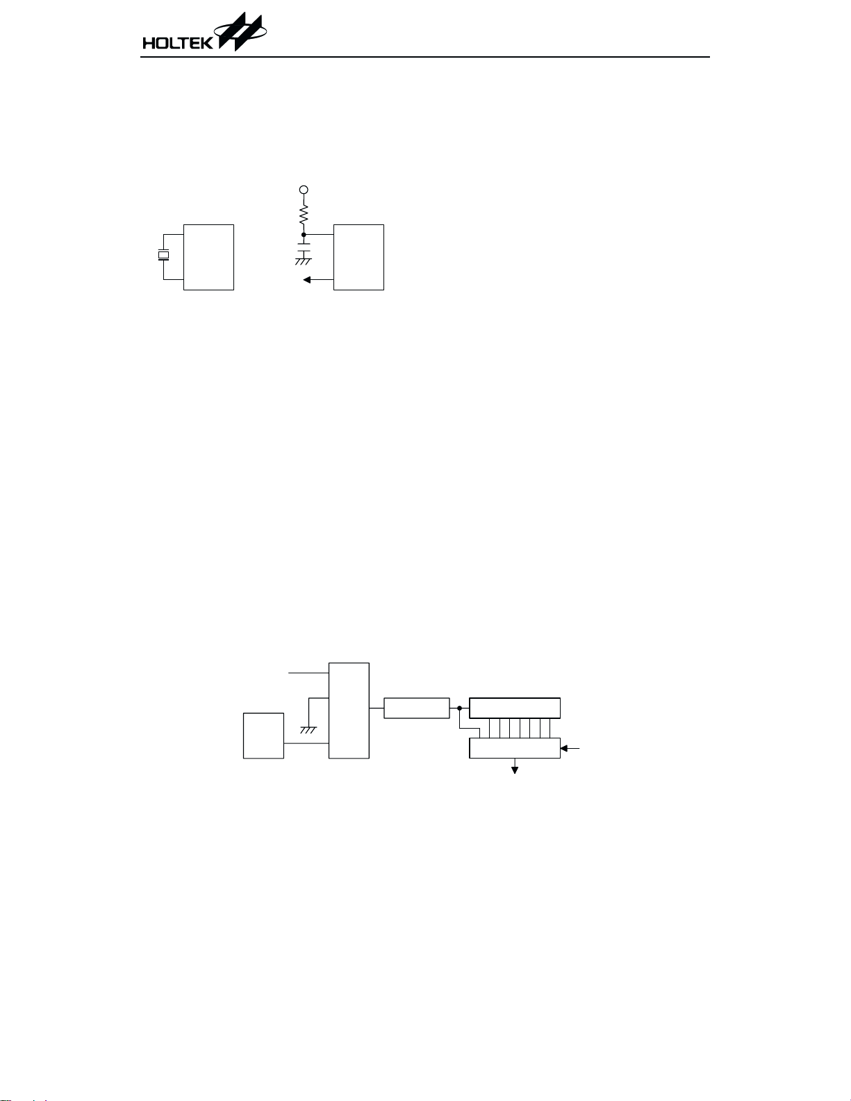
Oscillator configuration
There are two oscillator circuits in the
microcontroller.
V
DD
OSC1
OSC2
C rystal O scillator R C O scillator
470pF
f
/4
SYS
N M O S O pen D rain
OSC1
OSC2
System oscillator
Both are designed for system clocks, namely
the RC oscillator and the Crystal oscillator,
which are determined by the ROM code option.
No matter what oscillator type is selected, the
signal provides the system clock. The HALT
mode stops the system oscillator and ignores an
external signal to conserve power.
If an RC oscillator is used, an external resistor
between OSC1 and VDD is required and the
resistance must range from 51kW to 1MW. The
system clock, divided by 4, is available on
OSC2, which can be used to synchronize external logic. The RC oscillator provides the most
cost effective solution. However, the frequency
of oscillation may vary with VDD, temperatures and the chip itself due to process variations. It is, therefore, not suitable for timing
sensitive operations where an accurate oscillator frequency is desired.
If the Crystal oscillator is used, a crystal across
OSC1 and OSC2 is needed to provide the feed
back and phase shift required for the oscillator,
and no other external components are required.
Instead of a crystal, a resonator can also be con
nected between OSC1 and OSC2 to get a fre
quency reference, but two external capacitors
in OSC1 and OSC2 are required (If the oscillat
ing frequency is less than 1MHz).
The WDT oscillator is a free running on-chip RC
oscillator, and no external components are re
quired. Even if the system enters the power down
mode, the system clock is stopped, but the WDT
oscillator still works with a period of approxi
mately 65ms/5V. The WDT oscillator can be dis
abled by ROM code option to conserve power.
Watchdog timer - WDT
The clock source of WDT is implemented by a
dedicated RC oscillator (WDT oscillator) or in
struction clock (system clock divided by 4), de
cided by ROM code option. This timer is
designed to prevent a software malfunction or
sequence from jumping to an unknown location
with unpredictable results. The watchdog
timer can be disabled by a ROM code option. If
the watchdog timer is disabled, all the executions related to the WDT result in no operation.
Once the internal WDT oscillator (RC oscillator
with a period of 65ms/5V normally) is selected, it
is first divided by 256 (8-stage) to get the nominal time-out period of approximately
16.6ms/5V. This time-out period may vary with
temperatures, VDD and process variations. By
invoking the WDT prescaler, longer time-out
periods can be realized. Writing data to WS2,
WS1, WS0 (bit 2,1,0 of the WDTS) can give different time-out periods. If WS2, WS1, and WS0 are
all equal to 1, the division ratio is up to 1:128, and
-
-
-
-
-
-
-
-
-
S yste m C lock/4
WDT
OSC
ROM
C ode
Option
Select
W D T P re scaler
8-bit C ounter
7-bit C ounter
8-to-1 M U X
W D T Tim e-out
WS0~WS2
Watchdog timer
12 February 25, 2000

Preliminary
HT48R06A-1
the maximum time-out period is 2.2s/5V seconds.
If the WDT oscillator is disabled, the WDT clock
may still come from the instruction clock and op
erate in the same manner except that in the
HALT state the WDT may stop counting and lose
its protecting purpose. In this situation the logic
can only be restarted by external logic. The high
nibble and bit 3 of the WDTS are reserved for
user's defined flags, which can be used to indicate
some specified status.
If the device operates in a noisy environment, us
ing the on-chip RC oscillator (WDT OSC) is
strongly recommended, since the HALT will stop
the system clock.
WS2 WS1 WS0 Division Ratio
000 1:1
001 1:2
010 1:4
011 1:8
1 0 0 1:16
1 0 1 1:32
1 1 0 1:64
1 1 1 1:128
WDTS register
The WDT overflow under normal operation will
initialize "chip reset" and set the status bit
"TO". But in the HALT mode, the overflow will
initialize a ²warm reset², and only the PC and
SP are reset to zero. To clear the contents of
WDT (including the WDT prescaler), three
methods are adopted; external reset (a low level
), software instruction and a "HALT" in-
to RES
struction. The software instruction include
"CLR WDT" and the other set - "CLR WDT1"
and "CLR WDT2". Of these two types of instruc
tion, only one can be active depending on the
ROM code option - "CLR WDT times selection
option". If the "CLR WDT" is selected (i.e.
CLRWDT times equal one), any execution of
the "CLR WDT" instruction will clear the WDT.
In the case that "CLR WDT1" and "CLR WDT2"
are chosen (i.e. CLRWDT times equal two),
these two instructions must be executed to
clear the WDT; otherwise, the WDT may reset
the chip as a result of time-out.
Power down operation - HALT
The HALT mode is initialized by the "HALT" in
struction and results in the following...
·
The system oscillator will be turned off but
the WDT oscillator keeps running (if the
WDT oscillator is selected).
·
The contents of the on chip RAM and regis
ters remain unchanged.
·
WDT and WDT prescaler will be cleared and
-
-
recounted again (if the WDT clock is from the
WDT oscillator).
·
AlloftheI/Oportsmaintaintheiroriginalstatus.
·
The PD flag is set and the TO flag is cleared.
The system can leave the HALT mode by means
of an external reset, an interrupt, an external
falling edge signal on port Aor a WDT overflow.
An external reset causes a device initialization
and the WDT overflow performs a "warm re
set". After the TO and PD flags are examined,
the reason for chip reset can be determined.
The PD flag is cleared by system power-up or
executing the "CLR WDT" instruction and is set
when executing the "HALT" instruction. The
TO flag is set if the WDT time-out occurs, and
causes a wake-up that only resets the PC and
SP; the others keep their original status.
The port A wake-up and interrupt methods can
be considered as a continuation of normal execution. Each bit in port A can be independently
selected to wake up the device by the ROM code
option. Awakening from an I/O port stimulus,
the program will resume execution of the next
instruction. If it is awakening from an interrupt, two sequences may happen. If the related
interrupt is disabled or the interrupt is enabled
but the stack is full, the program will resume
execution at the next instruction. If the inter
rupt is enabled and the stack is not full, the reg
ular interrupt response takes place. If an
interrupt request flag is set to "1" before enter
ing the HALT mode, the wake-up function of
the related interrupt will be disabled. Once a
wake-up event occurs, it takes 1024 t
tem clock period) to resume normal operation.
In other words, a dummy period will be inserted
after wake-up. If the wake-up results from an
interrupt acknowledgment, the actual inter
rupt subroutine execution will be delayed by
one or more cycles. If the wake-up results in the
SYS
(sys
-
-
-
-
-
-
-
-
13 February 25, 2000
Preliminary
HT48R06A-1
next instruction execution, this will be executed
immediately after the dummy period is fin
ished.
To minimize power consumption, all the I/O
pins should be carefully managed before enter
ing the HALT status.
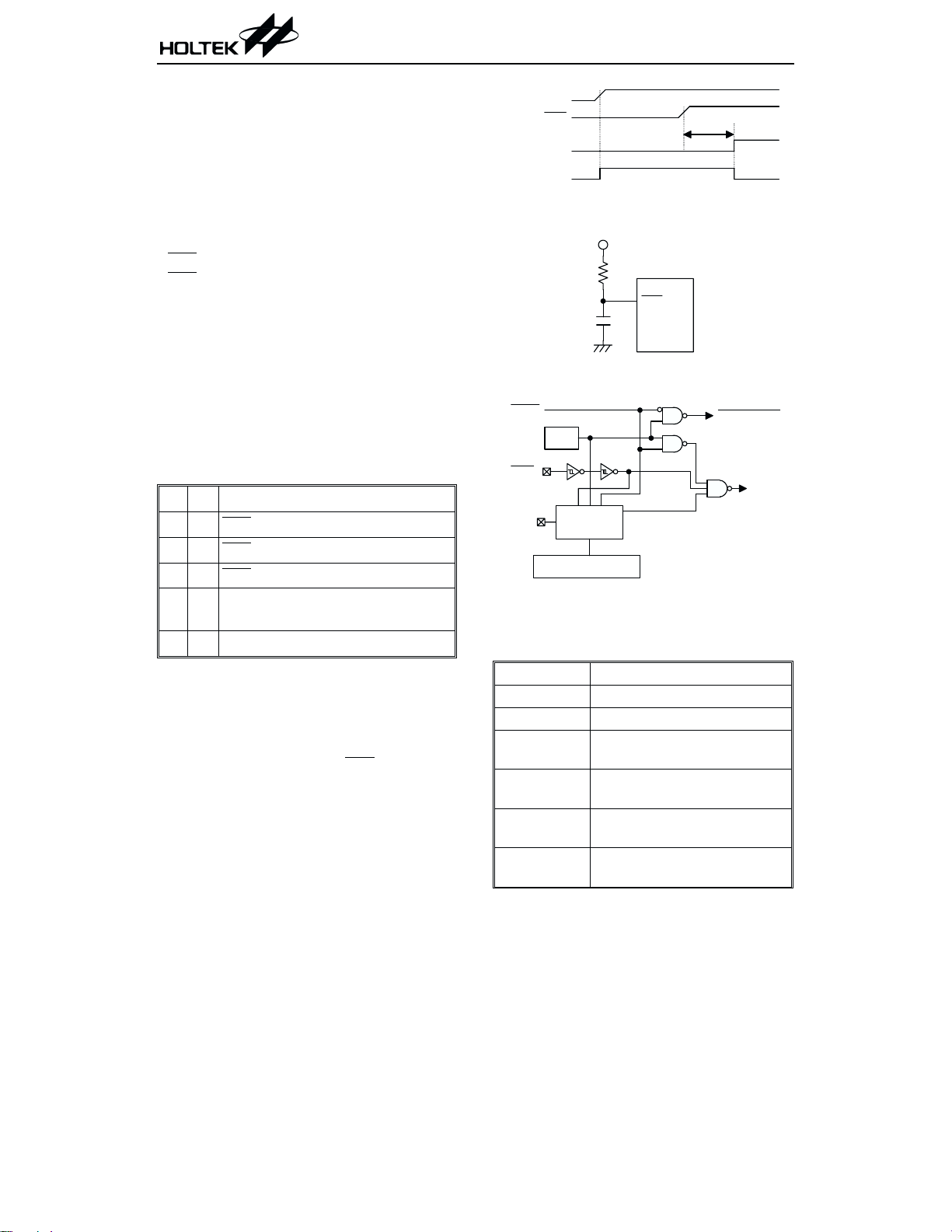
Reset
There are three ways in which a reset can occur:
·
RES reset during normal operation
·
RES reset during HALT
·
WDT time-out reset during normal operation
The WDT time-out during HALT is different
from other chip reset conditions, since it can
perform a "warm reset" that resets only the PC
and SP, leaving the other circuits in their origi
nal state. Some registers remain unchanged
during other reset conditions. Most registers
are reset to the ²initial condition² when the re
set conditions are met. By examining the PD
and TO flags, the program can distinguish be
tween different "chip resets".
TO PD RESET Conditions
0 0 RES
u u RES
0 1 RES
1u
reset during power-up
reset during normal operation
wake-up HALT
WDT time-out during normal operation
1 1 WDT wake-up HALT
Note: "u" means "unchanged"
To guarantee that the system oscillator is
started and stabilized, the SST (System
Start-up Timer) provides an extra-delay of 1024
system clock pulses when the system reset
(power-up, WDT time-out or RES
reset) or the
system awakes from the HALT state.
When a system reset occurs, the SST delay is
added during the reset period. Any wake-up
from HALT will enable the SST delay.
VDD
-
-
RES
SST Tim e-out
Chip Reset
t
SST
Reset timing chart
V
DD
RES
-
HALT
Reset circuit
-
WDT
-
RES
SST
OSC1
10-bit R ipple
C ounter
System R eset
Reset configuration
The functional unit chip reset status are shown
below.
PC 000H
Interrupt Disable
Prescaler Clear
WDT
Timer/event
Counter
Input/output
Ports
SP
Clear. After master reset,
WDT begins counting
Off
Input mode
Points to the top of
the stack
W arm R eset
Cold
Reset
14 February 25, 2000

Preliminary
The states of the registers is summarized in the table.
Register
TMR xxxx xxxx uuuu uuuu uuuu uuuu uuuu uuuu uuuu uuuu
TMRC 00-0 1000 00-0 1000 00-0 1000 00-0 1000 uu-u uuuu
Program
Counter
MP -xxx xxxx -uuu uuuu -uuu uuuu -uuu uuuu -uuu uuuu
ACC xxxx xxxx uuuu uuuu uuuu uuuu uuuu uuuu uuuu uuuu
TBLP xxxx xxxx uuuu uuuu uuuu uuuu uuuu uuuu uuuu uuuu
TBLH --xx xxxx --uu uuuu --uu uuuu --uu uuuu --uu uuuu
STATUS --00 xxxx --1u uuuu --uu uuuu --01 uuuu --11 uuuu
INTC --00 -000 --00 -000 --00 -000 --00 -000 --uu -uuu
WDTS 0000 0111 0000 0111 0000 0111 0000 0111 uuuu uuuu
PA 1111 1111 1111 1111 1111 1111 1111 1111 uuuu uuuu
PAC 1111 1111 1111 1111 1111 1111 1111 1111 uuuu uuuu
PB ---- -111 ---- -111 ---- -111 ---- -111 ---- -uuu
PBC ---- -111 ---- -111 ---- -111 ---- -111 ---- -uuu
PC ------11 ------11 ------11 ------11 ------uu
PCC ------11 ------11 ------11 ------11 ------uu
Reset
(Power On)
000H 000H 000H 000H 000H
WDT time-out
(Normal
Operation)
Reset
RES
(Normal
Operation)
RES
(HALT)
Reset
HT48R06A-1
WDT
Time-out
(HALT)*
Note: "*" means "warm reset"
"u" means "unchanged"
"x" means "unknown"
15 February 25, 2000

Preliminary
HT48R06A-1
Timer/event counter
A timer/event counter (TMR) is implemented in
the microcontroller. The timer/event counter
contains an 8-bit programmable count-up coun
ter and the clock may come from an external
source or the system clock.
Using the internal system clock, there is only
one reference time-base. The internal clock
source comes from f
. The external clock in
SYS
put allows the user to count external events,
measure time intervals or pulse widths, or to
generate an accurate time base.
There are 2 registers related to the timer/event
-
counter; TMR ([0DH]), TMRC ([0EH]). Two phys
ical registers are mapped to TMR location; writ
ing TMR makes the starting value be placed in
the timer/event counter preload register and
reading TMR gets the contents of the timer/event
counter. The TMRC is a timer/event counter con
trol register, which defines some options.
Label (TMRC) Bits Function
To define the prescaler stages, PSC2, PSC1, PSC0=
PSC0~PSC2 0~2
TE 3
TON 4
¾
5 Unused bits, read as"0"
000: f
INT=fSYS
001: f
INT=fSYS
010: f
INT=fSYS
011: f
INT=fSYS
100: f
INT=fSYS
101: f
INT=fSYS
110: f
INT=fSYS
111: f
INT=fSYS
To define the TMR active edge of timer/event counter
(0=active on low to high; 1=active on high to low)
To enable/disable timer counting
(0=disabled; 1=enabled)
/2
/4
/8
/16
/32
/64
/128
/256
To define the operating mode
TM0
TM1
01=Event count mode (external clock)
6
10=Timer mode (internal clock)
7
11=Pulse width measurement mode
00=Unused
-
-
-
f
SYS
8-stage prescaler
8-1 M U X
PSC2~PSC0
TM R
f
IN T
TM 1
TM 0
TO N
TMRC register
TM 1
TM 0
TE
Pulse W idth
M easurem ent
M ode C ontrol
Timer/event counter
16 February 25, 2000
Tim er/E vent C ounter
Preload R egister
Tim er/event
C ounter
Data Bus
R eload
1/2
O verflow
to Interrupt
BZ
BZ

Preliminary
HT48R06A-1
The TM0, TM1 bits define the operating mode.
The event count mode is used to count external
events, which means the clock source comes from
an external (TMR) pin. The timer mode functions
as a normal timer with the clock source coming
from the f
mode can be used to count the high or low level du
ration of the external signal (TMR). The counting
is based on the f
In the event count or timer mode, once the
timer/event counter starts counting, it will count
from the current contents in the timer/event
counter to FFH. Once overflow occurs, the coun
ter is reloaded from the timer/event counter
preload register and generates the interrupt re
quest flag (TF; bit 5 of INTC) at the same time.
In the pulse width measurement mode with
the TON and TE bits equal to one, once the
TMR has received a transient from low to high
(or high to low if the TE bits is "0") it will start
counting until the TMR returns to the original
level and resets the TON. The measured result
will remain in the timer/event counter even if
the activated transient occurs again. In other
words, only one cycle measurement can be
done. Until setting the TON, the cycle measurement will function again as long as it receives
further transient pulse. Note that, in this operating mode, the timer/event counter starts
counting not according to the logic level but according to the transient edges. In the case of
counter overflows, the counter is reloaded from
the timer/event counter preload register and issues the interrupt request just like the other
two modes. To enable the counting operation,
the timer ON bit (TON; bit 4 of TMRC) should
be set to 1. In the pulse width measurement
mode, the TON will be cleared automatically af
ter the measurement cycle is completed. But in
the other two modes the TON can only be reset
by instructions. The overflow of the timer/event
counter is one of the wake-up sources. No mat
ter what the operation mode is, writing a 0 to
ETI can disable the interrupt service.
In the case of timer/event counter OFF condi
tion, writing data to the timer/event counter
preload register will also reload that data to
the timer/event counter. But if the timer/event
clock. The pulse width measurement
INT
clock.
INT
counter is turned on, data written to it will only
be kept in the timer/event counter preload reg
ister. The timer/event counter will still operate
until overflow occurs. When the timer/event
counter (reading TMR) is read, the clock will be
blocked to avoid errors. As clock blocking may re
sults in a counting error, this must be taken into
consideration by the programmer.
The bit0~bit2 of the TMRC can be used to de
fine the pre-scaling stages of the internal clock
sources of timer/event counter. The definitions
are as shown. The overflow signal of
timer/event counter can be used to generate
PFD signals for buzzer driving.
-
Input/output ports
There are 13 bidirectional input/output lines in
the microcontroller, labeled from PA to PC, which
are mapped to the data memory of [12H], [14H]
and [16H] respectively. All of these I/O ports can
be used for input and output operations. For in
put operation, these ports are non-latching, that
is, the inputs must be ready at the T2 rising edge
of instruction "MOV A,[m]" (m=12H, 14H or
16H). For output operation, all the data is latched
and remains unchanged until the output latch is
rewritten.
Each I/O line has its own control register (PAC,
PBC, PCC) to control the input/output configuration. With this control register, CMOS output
or schmitt trigger input with or without
pull-high resistor structures can be reconfigured dynamically (i.e. on-the-fly) under software control. To function as an input, the
corresponding latch of the control register must
write "1". The input source also depends on the
control register. If the control register bit is "1",
the input will read the pad state. If the control
register bit is "0", the contents of the latches
will move to the internal bus. The latter is pos
sible in the "read-modify-write" instruction.
For output function, CMOS is the only configu
ration. These control registers are mapped to
locations 13H, 15H and 17H.
After a chip reset, these input/output lines re
main at high levels or floating state (dependent
on pull-high options). Each bit of these in
-
-
-
-
-
-
-
-
17 February 25, 2000

Preliminary
HT48R06A-1
put/output latches can be set or cleared by "SET
[m].i" and "CLR [m].i" (m=12H, 14H or 16H) in
structions.
Some instructions first input data and then fol
low the output operations. For example, "SET
[m].i", "CLR [m].i", "CPL [m]", "CPLA [m]" read
the entire port states into the CPU, execute the
defined operations (bit-operation), and then
write the results back to the latches or the accu
mulator.
Each line of port A has the capability of wak
ing-up the device. The highest 6-bit of port C and
5 bits of port B are not physically implemented;
on reading them a "0" is returned whereas writ
ing then results in a no-operation. See Applica
tion note.
There is a pull-high option available for all I/O
lines. Once the pull-high option is selected, all
I/O lines have pull-high resistors. Otherwise,
the pull-high resistors are absent. It should be
noted that a non-pull-high I/O line operating in
input mode will cause a floating state.
PB0
EXT
C ontrol B it
Q
D
QB
CK
S
Data Bit
Q
D
QB
CK
S
M
U
X
Data Bus
W rite C ontrol R egister
C hip R eset
R ead C ontrol R egister
W rite D ata R egister
(P B 0 , P B 1 O n ly )
R ead D ata R egister
System W ake-up
(P A only)
IN T fo r P C 0 O n ly
TM R for P C 1 O nly
E X T = B Z fo r P B 0 o n ly , E X T = B Z fo r P B 1 o n ly , c o n tro l= P B 0 d a ta re g is te r
Input/output ports
The PB0 and PB1 are pin-shared with BZ and
BZ
-
signal, respectively. If the BZ/BZ option is
selected, the output signal in output mode of
PB0/PB1 will be the PFD signal generated by
timer/event counter overflow signal. The input
mode always remaining its original functions.
Once the BZ/BZ
option is selected, the buzzer
output signals are controlled by PB0 data regis
ter only. The I/O functions of PB0/PB1 are
shown below.
PB0I/O IIIIOOOOOO
-
PB1 I/O I O O O I I I O O O
PB0/PB1 Mode x CBBCBBCBB
-
PB0 Data x x 0 1 D 0 1 D
-
PB1 Data x D xxxxxD
PB0 Pad Status IIIID0BD
PB1 Pad Status I D 0 B I I I D
Note: I: input; O: output; D, D0,D1: data;
B: buzzer option, BZ or BZ
C: CMOS output
V
DD
PU
PA0~PA7
PB0~PB2
PC0~PC1
M
U
X
EXTEN
(P B 0 , P B 1 O n ly )
OP0~OP7
01
0
xx
1
0B
0
0B
1
; x: don't care
-
18 February 25, 2000

Preliminary
HT48R06A-1
The PC0 and PC1 are pin-shared with INT,
TMR and pins respectively.
It is recommended that unused or not bonded
out I/O lines should be set as output pins by
software instruction to avoid consuming power
under input floating state.
ROM code option
The following table shows all kinds of ROM
code option in the microcontroller. All of the
ROM code options must be defined to ensure
proper system functioning.
Items Option
1 WDT clock source: WDTOSC/f
2 WDT enable/disable: enable/disable
3 LVD enable/disable: enable/disable
CLRWDT instruction(s)
4
: one/two clear WDT
instruction(s)
5 System oscillator: RC/Crystal
Pull-high resistors (PA~PC):
6
none/pull-high
7 BZ option: disable/enable
8 PA0~PA7 wake-up: disable/enable
9 Lock: unlock/lock
PROM programming and verification
The program memory used in the
microcontroller is arranged into a 1024´14 bits
program memory and a 3´8 bits option memory.
The program code and option code are stored in
the program and option memories. The pro
gramming of memories can be summarized in
nine steps as described below:
·
Power on (VDD=6.25V)
·
Set VPP (RES) to 12.5V
·
Set CS (PA5) to low
Let PA3~PA0 (AD3~AD0) be the address and
data bus and the PA4 (CLK) be the clock input.
The data on the AD3~AD0 pins will be clocked
into or out of the microcontroller on the falling
TID
edge of PA4 (CLK) for OTP programming and
verification.
The address data contains the code address (11
bits) and two option bits. A complete write cycle
will contain four CLK cycles. The first cycle,
bits 0~3 of the address are latched into the
device. The second and third cycles, bits 4~7
and bits 8~9 are latched respectively. The
fourth cycle, bit 2 is the TSEL option bit and bit
3 is the OSEL option bit. Bits 2~3 in the third
cycle and bits 0~1 in the fourth cycle are unde
fined. If the TSEL is "1" and the OSEL is "0",
the TEST memory will be read. If the TSEL is
"0" and the OSEL is "1", the option memory will
be accessed. If both the TSEL and OSEL are
"0", the program memory will be managed.
The code data is 14 bits wide. A complete
read/write cycle contains four CLK cycles. In
the first cycle, bits 0~3 of the code data are ac
cessed. In the second and third, bits 4~7 and
bits 8~11 are accessed respectively. In the
fourth cycle, bits 12~13 are accessed. Bits
14~15 are undefined. During code verification,
reading will return the result "00".
Select the TSEL and OSEL to program and
verify the program memory and option
memory. Use the R/W
programming or verification.
The address is incremented by one automatically after a code verification cycle. If the discontinued address programming or
verification is accomplished, the automatic addressing increment is disabled. For the discontinued address programming and verification,
the CS
gramming or verification cycle, that is, if a dis
continued address is managed, the
programming or verification cycle must be in
terrupted and restarted as well.
pin must return to high level for a pro-
(PA6) to select between
-
-
-
-
19 February 25, 2000

Preliminary
HT48R06A-1
The related pins of OTP programming and veri
fication are listed in the following table.
Pin
Name
Function Description
PA0 AD0 Bit 0 of address/data bus
PA1 AD1 Bit 1 of address/data bus
PA2 AD2 Bit 2 of address/data bus
PA3 AD3 Bit 3 of address/data bus
PA4 CLK
PA5 CS
PA6 R/W
RES
VPP
VPP
CS
R/W
Serial clock input for ad
dress and data
Chip select, active low
Read/write control input
Programming the power
supply
The timing charts of programming and verifica
tion are as shown. There is a LOCK signal for
code protection. If the LOCK is "1", reading the
code will return the result "1". However, if the
LOCK is "0", the code protection is disabled and
the code can be read always until the LOCK is
programmed as "1".
-
-
CLK
AD0
AD1
AD2
AD3
PC0 PC4 PC8
PC5
PC6
PC9
0OSEL
PC1
PC2
PC3 PC7
V e rific a tio n V e rific a tio n
0
D0
D4 D8
0
D1
D5
D9
TSEL0
D2
D6
D10
D3 D7
D11 0
Successive verification
20 February 25, 2000
D12 D0 D4 D8 D12
D13
D1 D5 D9 D13
0
D2 D6 D10 0
D3 D7 D11 0
PC incresing autom atically
D0
D1
D2
D3

VPP
CS
Preliminary
HT48R06A-1
R/W
V e rific a tio n V e rific a tio n V e rific a tio n
CLK
AD0
AD1
AD2
AD3
PC0~PC9 D0~D13 PC0~PC9 D0~D13 PC0~PC9 D0~D13
Non-successive verification
VPP
CS
R/W
CLK
AD0
AD1
AD2
AD3
t
CVS
t
CW S
t
CCS
PC0 PC4 PC8
PC1
PC2
PC3 PC7
PC5
PC6
t
CHP
0
0
PC9
TSEL0
0OSEL
t
CLP
D0
D4 D8
D1
D5
D2
D6
D3 D7
t
WP
D12 D0 D4 D8 D12
D9
D13
D10
0
D 11 0 or Lock
t
RCS
V e rific a tio nProgram m ing
t
t
CRS
t
DCS
WCS
D1 D5 D9 D13
D2 D6 D10 0
D3 D7 D11 0
Code programming and verification
21 February 25, 2000

VPP
CS
Preliminary
HT48R06A-1
R/W
CLK
AD0
AD1
AD2
AD3
Progrm m ing Progrm m ing
PC0~PC9 D0~D13 D0~D13 PC0~PC9 D0~D13 D0~D13
V e rific a tio n V e rific a tio n
Non-successive programming and verification
VPP
CS
R/W
CLK
AD0
AD 1, A D 2, A D 3 : don't care
ID0ID1ID2ID3ID4ID5ID6ID7
ID code verification
22 February 25, 2000

VPP
CS
Preliminary
HT48R06A-1
R/W
CLK
AD0
AD1
AD2
AD3
Progrm m ing Progrm m ing
PC0~PC9 D 0~D 13 D0~D13 D0~D13D0~D13
V e rific a tio n V e rific a tio n
Successive programming and verification
Application Circuits
R C o s c illa to r fo r m u ltip le I/O a p p lic a tio n s
V
DD
0.1mF
51kW~
1M
W
470pF
f
SYS
100k
0.1mF
OSC1
/4
OSC2
V
DD
W
HT48R06A-1
RES
PA0~PA7
PB0/BZ
PB1/BZ
PB2
PC0/IN T
PC1/TM R
V e rific a tio nProgrm m ing
PC + 1 autom atically P C + 1 autom atically
D0~D13D0~D13
C ry s ta l o s c illa to r fo r m u lt ip le I/O a p p lic a tio n s
C1
C2
OSC1
OSC2
V
DD
HT48R06A-1
0.1mF
100k
W
RES
0.1mF
PA0~PA7
PB0/BZ
PB1/BZ
PB2
P C 0 /IN T
PC1/TM R
N ote: The resistance and capacitance
for reset circuit should be designed
to ensure that the V D D is stable and
rem ains in a valid range of the operating
voltage before bringing R E S to high.
Note:C1=C2=300pF if f
O therw ise, C
SYS
1 =C 2 =0.
<1M H z
23 February 25, 2000

Instruction Set Summary
Preliminary
HT48R06A-1
Mnemonic Description
Arithmetic
ADD A,[m]
ADDM A,[m]
ADD A,x
ADC A,[m]
ADCM A,[m]
SUB A,x
SUB A,[m]
SUBM A,[m]
Add data memory to ACC
Add ACC to data memory
Add immediate data to ACC
Add data memory to ACC with carry
Add ACC to register with carry
Subtract immediate data from ACC
Subtract data memory from ACC
Subtract data memory from ACC with result in data
memory
SBC A,[m]
SBCM A,[m]
Subtract data memory from ACC with carry
Subtract data memory from ACC with carry and result
in data memory
DAA [m]
Decimal adjust ACC for addition with result in data
memory
Logic Operation
AND A,[m]
OR A,[m]
XOR A,[m]
ANDM A,[m]
ORM A,[m]
XORM A,[m]
AND A,x
OR A,x
XOR A,x
CPL [m]
CPLA [m]
AND data memory to ACC
OR data memory to ACC
Exclusive-OR data memory to ACC
AND ACC to data memory
OR ACC to data memory
Exclusive-OR ACC to data memory
AND immediate data to ACC
OR immediate data to ACC
Exclusive-OR immediate data to ACC
Complement data memory
Complement data memory with result in ACC
Increment & Decrement
INCA [m]
INC [m]
DECA [m]
DEC [m]
Increment data memory with result in ACC
Increment data memory
Decrement data memory with result in ACC
Decrement data memory
Instruction
Cycle
1
(1)
1
1
1
(1)
1
1
1
(1)
1
1
1(1)
(1)
1
1
1
1
(1)
1
(1)
1
(1)
1
1
1
1
(1)
1
1
1
(1)
1
1
(1)
1
Flag
Affected
Z,C,AC,OV
Z,C,AC,OV
Z,C,AC,OV
Z,C,AC,OV
Z,C,AC,OV
Z,C,AC,OV
Z,C,AC,OV
Z,C,AC,OV
Z,C,AC,OV
Z,C,AC,OV
C
Z
Z
Z
Z
Z
Z
Z
Z
Z
Z
Z
Z
Z
Z
Z
24 February 25, 2000

Preliminary
HT48R06A-1
Mnemonic Description
Rotate
RRA [m]
RR [m]
RRCA [m]
Rotate data memory right with result in ACC
Rotate data memory right
Rotate data memory right through carry with result in
ACC
RRC [m]
RLA [m]
RL [m]
RLCA [m]
Rotate data memory right through carry
Rotate data memory left with result in ACC
Rotate data memory left
Rotate data memory left through carry with result in
ACC
RLC [m]
Rotate data memory left through carry
Data Move
MOV A,[m]
MOV [m],A
MOV A,x
Move data memory to ACC
Move ACC to data memory
Move immediate data to ACC
Bit Operation
CLR [m].i
SET [m].i
Clear bit of data memory
Set bit of data memory
Branch
JMP addr
SZ [m]
SZA [m]
Jump unconditionally
Skip if data memory is zero
Skip if data memory is zero with data movement to
ACC
SZ [m].i
SNZ [m].i
SIZ [m]
SDZ [m]
SIZA [m]
Skip if bit i of data memory is zero
Skip if bit i of data memory is not zero
Skip if increment data memory is zero
Skip if decrement data memory is zero
Skip if increment data memory is zero with result in
ACC
SDZA [m]
Skip if decrement data memory is zero with result in
ACC
CALL addr
RET
RET A,x
Subroutine call
Return from subroutine
Return from subroutine and load immediate data to
ACC
RETI
Return from interrupt
Instruction
Cycle
1
(1)
1
1
(1)
1
1
(1)
1
1
(1)
1
1
(1)
1
1
(1)
1
(1)
1
2
(2)
1
(2)
1
(2)
1
(2)
1
(3)
1
(3)
1
(2)
1
(2)
1
2
2
2
2
Flag
Affected
None
None
C
C
None
None
C
C
None
None
None
None
None
None
None
None
None
None
None
None
None
None
None
None
None
None
25 February 25, 2000

Preliminary
HT48R06A-1
Mnemonic Description
Table Read
TABRDC [m]
Read ROM code (current page) to data memory and
TBLH
TABRDL [m]
Read ROM code (last page) to data memory and TBLH
Miscellaneous
NOP
CLR [m]
SET [m]
CLR WDT
CLR WDT1
CLR WDT2
SWAP [m]
SWAPA [m]
HALT
No operation
Clear data memory
Set data memory
Clear watchdog timer
Pre-clear watchdog timer
Pre-clear watchdog timer
Swap nibbles of data memory
Swap nibbles of data memory with result in ACC
Enter power down mode
Note: x: 8 bits immediate data
m: Data memory address
A: Accumulator
i: 0~7 number of bits
addr: Program memory address
Ö: Flag is affected
-: Flag is not affected
(1)
: If a loading to the PCL register occurs, the execution cycle of instructions will be delayed
one more cycle (four system clocks).
(2)
: If a skipping to next instruction occurs, the execution cycle of instructions will be delayed
one more cycle (four system clocks). Otherwise the original instruction cycle is unchanged.
(3):(1)
(4)
: The flags may be affected by the execution status. If the watchdog timer is cleared by
and
(2)
executing the CLR WDT1 or CLR WDT2 instruction, the TO is set and the PD is cleared.
Otherwise the TO and PD flags remain unchanged.
Instruction
Cycle
(1)
2
(1)
2
1
(1)
1
(1)
1
1
1
1
(1)
1
1
1
Flag
Affected
None
None
None
None
None
TO,PD
(4)
TO
,PD
(4)
TO
,PD
None
None
TO,PD
(4)
(4)
26 February 25, 2000

Preliminary
HT48R06A-1
Instruction Definition
ADC A,[m] Add data memory and carry to the accumulator
Description The contents of the specified data memory, accumulator and the carry flag
are added simultaneously, leaving the result in the accumulator.
Operation
Affected flag(s)
ADCM A,[m] Add the accumulator and carry to data memory
Description The contents of the specified data memory, accumulator and the carry flag
Operation
Affected flag(s)
ADD A,[m] Add data memory to the accumulator
Description The contents of the specified data memory and the accumulator are added.
Operation
Affected flag(s)
ACC ¬ ACC+[m]+C
TC2 TC1 TO PD OV Z AC C
¾¾¾¾ÖÖÖÖ
are added simultaneously, leaving the result in the specified data memory.
[m] ¬ ACC+[m]+C
TC2 TC1 TO PD OV Z AC C
¾¾¾¾ÖÖÖÖ
The result is stored in the accumulator.
ACC ¬ ACC+[m]
TC2 TC1 TO PD OV Z AC C
¾¾¾¾ÖÖÖÖ
ADD A,x Add immediate data to the accumulator
Description The contents of the accumulator and the specified data are added, leaving
the result in the accumulator.
Operation
Affected flag(s)
ACC ¬ ACC+x
TC2 TC1 TO PD OV Z AC C
¾¾¾¾ÖÖÖÖ
27 February 25, 2000

Preliminary
ADDM A,[m] Add the accumulator to the data memory
Description The contents of the specified data memory and the accumulator are added.
The result is stored in the data memory.
Operation
Affected flag(s)
AND A,[m] Logical AND accumulator with data memory
Description Data in the accumulator and the specified data memory perform a bitwise
Operation
Affected flag(s)
AND A,x Logical AND immediate data to the accumulator
Description Data in the accumulator and the specified data perform a bitwise logi
Operation
Affected flag(s)
[m] ¬ ACC+[m]
TC2 TC1 TO PD OV Z AC C
¾¾¾¾ÖÖÖÖ
logical_AND operation. The result is stored in the accumulator.
ACC ¬ ACC "AND" [m]
TC2 TC1 TO PD OV Z AC C
¾¾¾¾¾Ö¾¾
cal_AND operation. The result is stored in the accumulator.
ACC ¬ ACC "AND" x
TC2 TC1 TO PD OV Z AC C
¾¾¾¾¾Ö¾¾
HT48R06A-1
-
ANDM A,[m] Logical AND data memory with the accumulator
Description Data in the specified data memory and the accumulator perform a bitwise
logical_AND operation. The result is stored in the data memory.
Operation
Affected flag(s)
[m] ¬ ACC "AND" [m]
TC2 TC1 TO PD OV Z AC C
¾¾¾¾¾Ö¾¾
28 February 25, 2000

Preliminary
CALL addr Subroutine call
Description The instruction unconditionally calls a subroutine located at the indicated
address. The program counter increments once to obtain the address of the
next instruction, and pushes this onto the stack. The indicated address is
then loaded. Program execution continues with the instruction at this ad
dress.
Operation
Affected flag(s)
CLR [m] Clear data memory
Description The contents of the specified data memory are cleared to zero.
Operation
Affected flag(s)
CLR [m].i Clear bit of data memory
Description The bit i of the specified data memory is cleared to zero.
Operation
Affected flag(s)
Stack ¬ PC+1
PC ¬ addr
TC2 TC1 TO PD OV Z AC C
¾¾¾¾¾¾¾¾
[m] ¬ 00H
TC2 TC1 TO PD OV Z AC C
¾¾¾¾¾¾¾¾
[m].i ¬ 0
TC2 TC1 TO PD OV Z AC C
¾¾¾¾¾¾¾¾
HT48R06A-1
-
CLR WDT Clear watchdog timer
Description The WDT and the WDT Prescaler are cleared (re-counting from zero). The
power down bit (PD) and time-out bit (TO) are cleared.
Operation
Affected flag(s)
WDT and WDT Prescaler ¬ 00H
PD and TO ¬ 0
TC2 TC1 TO PD OV Z AC C
¾¾
00
29 February 25, 2000
¾¾¾¾

Preliminary
CLR WDT1 Preclear watchdog timer
Description The TD, PD flags, WDT and the WDT Prescaler has cleared (re-counting
from zero), if the other preclear WDT instruction has been executed. Only ex
ecution of this instruction without the other preclear instruction just sets the
indicated flag which implies this instruction has been executed and the TO
and PD flags remain unchanged.
Operation
Affected flag(s)
CLR WDT2 Preclear watchdog timer
Description The TO, PD flags, WDT and the WDT Prescaler are cleared (re-counting
Operation
Affected flag(s)
WDT and WDT Prescaler ¬ 00H*
PD and TO ¬ 0*
TC2 TC1 TO PD OV Z AC C
¾¾
from zero), if the other preclear WDT instruction has been executed. Only ex
ecution of this instruction without the other preclear instruction, sets the in
dicated flag which implies this instruction has been executed and the TO and
PD flags remain unchanged.
WDT and WDT Prescaler ¬ 00H*
PD and TO ¬ 0*
TC2 TC1 TO PD OV Z AC C
¾¾
0* 0*
0* 0*
¾¾¾¾
¾¾¾¾
HT48R06A-1
-
-
-
CPL [m] Complement data memory
Description Each bit of the specified data memory is logically complemented (1's comple-
ment). Bits which previously contained a one are changed to zero and
vice-versa.
Operation
Affected flag(s)
[m] ¬ [m
TC2 TC1 TO PD OV Z AC C
]
¾¾¾¾¾Ö¾¾
30 February 25, 2000

Preliminary
CPLA [m] Complement data memory and place result in the accumulator
Description Each bit of the specified data memory is logically complemented (1's comple
ment). Bits which previously contained a one are changed to zero and
vice-versa. The complemented result is stored in the accumulator and the
contents of the data memory remain unchanged.
Operation
Affected flag(s)
DAA [m] Decimal-Adjust accumulator for addition
Description The accumulator value is adjusted to the BCD (Binary Code Decimal) code.
Operation If ACC.3~ACC.0 >9 or AC=1
Affected flag(s)
ACC ¬ [m
TC2 TC1 TO PD OV Z AC C
¾¾¾¾¾Ö¾¾
The accumulator is divided into two nibbles. Each nibble is adjusted to the
BCD code and an internal carry (AC1) will be done if the low nibble of the ac
cumulator is greater than 9. The BCD adjustment is done by adding 6 to the
original value if the original value is greater than 9 or a carry (AC or C) is set;
otherwise the original value remains unchanged. The result is stored in the
data memory and only the carry flag (C) may be affected.
then [m].3~[m].0 ¬ (ACC.3~ACC.0)+6, AC1=AC
else [m].3~[m].0) ¬ (ACC.3~ACC.0), AC1=0
and
If ACC.7~ACC.4+AC1 >9 or C=1
then [m].7~[m].4 ¬ ACC.7~ACC.4+6+AC1,C=1
else [m].7~[m].4 ¬ ACC.7~ACC.4+AC1,C=C
TC2 TC1 TO PD OV Z AC C
¾¾¾¾¾¾¾ Ö
]
HT48R06A-1
-
-
DEC [m] Decrement data memory
Description Data in the specified data memory is decremented by one
Operation
Affected flag(s)
[m] ¬ [m]-1
TC2 TC1 TO PD OV Z AC C
¾¾¾¾¾Ö¾¾
31 February 25, 2000

Preliminary
DECA [m] Decrement data memory and place result in the accumulator
Description Data in the specified data memory is decremented by one, leaving the result
in the accumulator. The contents of the data memory remain unchanged.
Operation
Affected flag(s)
HALT Enter power down mode
Description This instruction stops program execution and turns off the system clock. The
Operation
Affected flag(s)
ACC ¬ [m]-1
TC2 TC1 TO PD OV Z AC C
¾¾¾¾¾Ö¾¾
contents of the RAM and registers are retained. The WDT and prescaler are
cleared. The power down bit (PD) is set and the WDT time-out bit (TO) is
cleared.
PC ¬ PC+1
PD ¬ 1
TO ¬ 0
TC2 TC1 TO PD OV Z AC C
¾¾
01
¾¾¾¾
HT48R06A-1
INC [m] Increment data memory
Description Data in the specified data memory is incremented by one
Operation
Affected flag(s)
INCA [m] Increment data memory and place result in the accumulator
Description Data in the specified data memory is incremented by one, leaving the result
Operation
Affected flag(s)
[m] ¬ [m]+1
TC2 TC1 TO PD OV Z AC C
¾¾¾¾¾Ö¾¾
in the accumulator. The contents of the data memory remain unchanged.
ACC ¬ [m]+1
TC2 TC1 TO PD OV Z AC C
¾¾¾¾¾Ö¾¾
32 February 25, 2000

Preliminary
JMP addr Directly jump
Description Bits of the program counter are replaced with the directly-specified address
unconditionally, and control is passed to this destination.
Operation
Affected flag(s)
MOV A,[m] Move data memory to the accumulator
Description The contents of the specified data memory are copied to the accumulator.
Operation
Affected flag(s)
MOV A,x Move immediate data to the accumulator
Description The 8-bit data specified by the code is loaded into the accumulator.
Operation
Affected flag(s)
PC ¬ addr
TC2 TC1 TO PD OV Z AC C
¾¾¾¾¾¾¾¾
ACC ¬ [m]
TC2 TC1 TO PD OV Z AC C
¾¾¾¾¾¾¾¾
ACC ¬ x
TC2 TC1 TO PD OV Z AC C
¾¾¾¾¾¾¾¾
HT48R06A-1
MOV [m],A Move the accumulator to data memory
Description The contents of the accumulator are copied to the specified data memory (one
of the data memory).
Operation
Affected flag(s)
NOP No operation
Description No operation is performed. Execution continues with the next instruction.
Operation
Affected flag(s)
[m] ¬ ACC
TC2 TC1 TO PD OV Z AC C
¾¾¾¾¾¾¾¾
PC ¬ PC+1
TC2 TC1 TO PD OV Z AC C
¾¾¾¾¾¾¾¾
33 February 25, 2000

Preliminary
OR A,[m] Logical OR accumulator with data memory
Description Data in the accumulator and the specified data memory (one of the data
memory) perform a bitwise logical_OR operation. The result is stored in the
accumulator.
Operation
Affected flag(s)
OR A,x Logical OR immediate data to the accumulator
Description Data in the accumulator and the specified data perform a bitwise logical_OR
Operation
Affected flag(s)
ORM A,[m] Logical OR data memory with the accumulator
Description Data in the data memory (one of the data memory) and the accumulator per
Operation
Affected flag(s)
ACC ¬ ACC "OR" [m]
TC2 TC1 TO PD OV Z AC C
¾¾¾¾¾Ö¾¾
operation. The result is stored in the accumulator.
ACC ¬ ACC "OR" x
TC2 TC1 TO PD OV Z AC C
¾¾¾¾¾Ö¾¾
form a bitwise logical_OR operation. The result is stored in the data memory.
[m] ¬ ACC "OR" [m]
TC2 TC1 TO PD OV Z AC C
¾¾¾¾¾Ö¾¾
HT48R06A-1
-
RET Return from subroutine
Description The program counter is restored from the stack. This is a two cycle instruc-
tion.
Operation
Affected flag(s)
PC ¬ Stack
TC2 TC1 TO PD OV Z AC C
¾¾¾¾¾¾¾¾
34 February 25, 2000

Preliminary
RET A,x Return and place immediate data in the accumulator
Description The program counter is restored from the stack and the accumulator loaded
with the specified 8-bit immediate data.
Operation
Affected flag(s)
RETI Return from interrupt
Description The program counter is restored from the stack, and interrupts are enabled
Operation
Affected flag(s)
RL [m] Rotate data memory left
Description The contents of the specified data memory are rotated one bit left with bit 7
Operation
Affected flag(s)
PC ¬ Stack
ACC ¬ x
TC2 TC1 TO PD OV Z AC C
¾¾¾¾¾¾¾¾
by setting the EMI bit. EMI is the enable master (global) interrupt bit (bit 0;
register INTC).
PC ¬ Stack
EMI ¬ 1
TC2 TC1 TO PD OV Z AC C
¾¾¾¾¾¾¾¾
rotated into bit 0.
[m].(i+1) ¬ [m].i; [m].i:bit i of the data memory (i=0~6)
[m].0 ¬ [m].7
TC2 TC1 TO PD OV Z AC C
¾¾¾¾¾¾¾¾
HT48R06A-1
RLA [m] Rotate data memory left and place result in the accumulator
Description Data in the specified data memory is rotated one bit left with bit 7 rotated
into bit 0, leaving the rotated result in the accumulator. The contents of the
data memory remain unchanged.
Operation
Affected flag(s)
ACC.(i+1) ¬ [m].i; [m].i:bit i of the data memory (i=0~6)
ACC.0 ¬ [m].7
TC2 TC1 TO PD OV Z AC C
¾¾¾¾¾¾¾¾
35 February 25, 2000

Preliminary
RLC [m] Rotate data memory left through carry
Description The contents of the specified data memory and the carry flag are rotated one
bit left. Bit 7 replaces the carry bit; the original carry flag is rotated into the
bit 0 position.
Operation
Affected flag(s)
RLCA [m] Rotate left through carry and place result in the accumulator
Description Data in the specified data memory and the carry flag are rotated one bit left.
Operation
Affected flag(s)
[m].(i+1) ¬ [m].i; [m].i:bit i of the data memory (i=0~6)
[m].0 ¬ C
C ¬ [m].7
TC2 TC1 TO PD OV Z AC C
¾¾¾¾¾¾¾ Ö
Bit 7 replaces the carry bit and the original carry flag is rotated into bit 0 po
sition. The rotated result is stored in the accumulator but the contents of the
data memory remain unchanged.
ACC.(i+1) ¬ [m].i; [m].i:bit i of the data memory (i=0~6)
ACC.0 ¬ C
C ¬ [m].7
TC2 TC1 TO PD OV Z AC C
¾¾¾¾¾¾¾ Ö
HT48R06A-1
-
RR [m] Rotate data memory right
Description The contents of the specified data memory are rotated one bit right with bit 0
rotated to bit 7.
Operation
Affected flag(s)
[m].i ¬ [m].(i+1); [m].i:bit i of the data memory (i=0~6)
[m].7 ¬ [m].0
TC2 TC1 TO PD OV Z AC C
¾¾¾¾¾¾¾¾
36 February 25, 2000

Preliminary
RRA [m] Rotate right and place result in the accumulator
Description Data in the specified data memory is rotated one bit right with bit 0 rotated
into bit 7, leaving the rotated result in the accumulator. The contents of the
data memory remain unchanged.
Operation
Affected flag(s)
RRC [m] Rotate data memory right through carry
Description The contents of the specified data memory and the carry flag are together ro
Operation
Affected flag(s)
ACC.(i) ¬ [m].(i+1); [m].i:bit i of the data memory (i=0~6)
ACC.7 ¬ [m].0
TC2 TC1 TO PD OV Z AC C
¾¾¾¾¾¾¾¾
tated one bit right. Bit 0 replaces the carry bit; the original carry flag is ro
tated into the bit 7 position.
[m].i ¬ [m].(i+1); [m].i:bit i of the data memory (i=0~6)
[m].7 ¬ C
C ¬ [m].0
TC2 TC1 TO PD OV Z AC C
¾¾¾¾¾¾¾ Ö
HT48R06A-1
-
-
RRCA [m] Rotate right through carry and place result in the accumulator
Description Data of the specified data memory and the carry flag are rotated one bit
right. Bit 0 replaces the carry bit and the original carry flag is rotated into
the bit 7 position. The rotated result is stored in the accumulator. The contents of the data memory remain unchanged.
Operation
Affected flag(s)
ACC.i ¬ [m].(i+1); [m].i:bit i of the data memory (i=0~6)
ACC.7 ¬ C
C ¬ [m].0
TC2 TC1 TO PD OV Z AC C
¾¾¾¾¾¾¾ Ö
37 February 25, 2000

Preliminary
SBC A,[m] Subtract data memory and carry from the accumulator
Description The contents of the specified data memory and the complement of the carry
flag are subtracted from the accumulator, leaving the result in the accumula
tor.
Operation
Affected flag(s)
SBCM A,[m] Subtract data memory and carry from the accumulator
Description The contents of the specified data memory and the complement of the carry
Operation
Affected flag(s)
SDZ [m] Skip if decrement data memory is zero
Description The contents of the specified data memory are decremented by one. If the re
Operation
Affected flag(s)
ACC ¬ ACC+[m
TC2 TC1 TO PD OV Z AC C
¾¾¾¾ÖÖÖÖ
flag are subtracted from the accumulator, leaving the result in the data
memory.
[m] ¬ ACC+[m
TC2 TC1 TO PD OV Z AC C
¾¾¾¾ÖÖÖÖ
sult is zero, the next instruction is skipped. If the result is zero, the following
instruction, fetched during the current instruction execution, is discarded
and a dummy cycle is replaced to get the proper instruction (two cycles). Otherwise proceed with the next instruction (one cycle).
Skip if ([m]-1)=0, [m] ¬ ([m]-1)
TC2 TC1 TO PD OV Z AC C
¾¾¾¾¾¾¾¾
]+C
]+C
HT48R06A-1
-
-
SDZA [m] Decrement data memory and place result in ACC, skip if zero
Description The contents of the specified data memory are decremented by one. If the re
sult is zero, the next instruction is skipped. The result is stored in the accu
mulator but the data memory remains unchanged. If the result is zero, the
following instruction, fetched during the current instruction execution, is
discarded and a dummy cycle is replaced to get the proper instruction (two
cycles). Otherwise proceed with the next instruction (one cycle).
Operation
Affected flag(s)
Skip if ([m]-1)=0, ACC ¬ ([m]-1)
TC2 TC1 TO PD OV Z AC C
¾¾¾¾¾¾¾¾
38 February 25, 2000
-
-

Preliminary
SET [m] Set data memory
Description Each bit of the specified data memory is set to one.
Operation
Affected flag(s)
SET [m].i Set bit of data memory
Description Bit "i" of the specified data memory is set to one.
Operation
Affected flag(s)
SIZ [m] Skip if increment data memory is zero
Description The contents of the specified data memory are incremented by one. If the re
Operation
Affected flag(s)
[m] ¬ FFH
TC2 TC1 TO PD OV Z AC C
¾¾¾¾¾¾¾¾
[m].i ¬ 1
TC2 TC1 TO PD OV Z AC C
¾¾¾¾¾¾¾¾
sult is zero, the following instruction, fetched during the current instruction
execution, is discarded and a dummy cycle is replaced to get the proper in
struction (two cycles). Otherwise proceed with the next instruction (one cy
cle).
Skip if ([m]+1)=0, [m] ¬ ([m]+1)
TC2 TC1 TO PD OV Z AC C
¾¾¾¾¾¾¾¾
HT48R06A-1
-
-
-
SIZA [m] Increment data memory and place result in ACC, skip if zero
Description The contents of the specified data memory are incremented by one. If the re-
sult is zero, the next instruction is skipped and the result is stored in the accumulator. The data memory remains unchanged. If the result is zero, the
following instruction, fetched during the current instruction execution, is
discarded and a dummy cycle is replaced to get the proper instruction (two
cycles). Otherwise proceed with the next instruction (one cycle).
Operation
Affected flag(s)
Skip if ([m]+1)=0, ACC ¬ ([m]+1)
TC2 TC1 TO PD OV Z AC C
¾¾¾¾¾¾¾¾
39 February 25, 2000

Preliminary
SNZ [m].i Skip if bit "i" of the data memory is not zero
Description If bit "i" of the specified data memory is not zero, the next instruction is
skipped. If bit "i" of the data memory is not zero, the following instruction,
fetched during the current instruction execution, is discarded and a dummy
cycle is replaced to get the proper instruction (two cycles). Otherwise proceed
with the next instruction (one cycle).
Operation
Affected flag(s)
SUB A,[m] Subtract data memory from the accumulator
Description The specified data memory is subtracted from the contents of the accumula
Operation
Affected flag(s)
SUBM A,[m] Subtract data memory from the accumulator
Description The specified data memory is subtracted from the contents of the accumula
Operation
Affected flag(s)
Skip if [m].i¹0
TC2 TC1 TO PD OV Z AC C
¾¾¾¾¾¾¾¾
tor, leaving the result in the accumulator.
ACC ¬ ACC+[m
TC2 TC1 TO PD OV Z AC C
¾¾¾¾ÖÖÖÖ
tor, leaving the result in the data memory.
[m] ¬ ACC+[m
TC2 TC1 TO PD OV Z AC C
¾¾¾¾ÖÖÖÖ
]+1
]+1
HT48R06A-1
-
-
SUB A,x Subtract immediate data from the accumulator
Description The immediate data specified by the code is subtracted from the contents of
the accumulator, leaving the result in the accumulator.
Operation
Affected flag(s)
ACC ¬ ACC+x
TC2 TC1 TO PD OV Z AC C
¾¾¾¾ÖÖÖÖ
+1
40 February 25, 2000

Preliminary
SWAP [m] Swap nibbles within the data memory
Description The low-order and high-order nibbles of the specified data memory (one of
the data memories) are interchanged.
Operation
Affected flag(s)
SWAPA [m] Swap data memory and place result in the accumulator
Description The low-order and high-order nibbles of the specified data memory are inter
Operation
Affected flag(s)
SZ [m] Skip if data memory is zero
Description If the contents of the specified data memory are zero, the following instruc
Operation Skip if [m]=0
Affected flag(s)
[m].3~[m].0 « [m].7~[m].4
TC2 TC1 TO PD OV Z AC C
¾¾¾¾¾¾¾¾
changed, writing the result to the accumulator. The contents of the data
memory remain unchanged.
ACC.3~ACC.0 ¬ [m].7~[m].4
ACC.7~ACC.4 ¬ [m].3~[m].0
TC2 TC1 TO PD OV Z AC C
¾¾¾¾¾¾¾¾
tion, fetched during the current instruction execution, is discarded and a
dummy cycle is replaced to get the proper instruction (two cycles). Otherwise
proceed with the next instruction (one cycle).
TC2 TC1 TO PD OV Z AC C
¾¾¾¾¾¾¾¾
HT48R06A-1
-
-
SZA [m] Move data memory to ACC, skip if zero
Description The contents of the specified data memory are copied to the accumulator. If
the contents is zero, the following instruction, fetched during the current in
struction execution, is discarded and a dummy cycle is replaced to get the
proper instruction (two cycles). Otherwise proceed with the next instruction
(one cycle).
Operation Skip if [m]=0
Affected flag(s)
TC2 TC1 TO PD OV Z AC C
¾¾¾¾¾¾¾¾
41 February 25, 2000
-

Preliminary
SZ [m].i Skip if bit "i" of the data memory is zero
Description If bit "i" of the specified data memory is zero, the following instruction,
fetched during the current instruction execution, is discarded and a dummy
cycle is replaced to get the proper instruction (two cycles). Otherwise proceed
with the next instruction (one cycle).
Operation Skip if [m].i=0
Affected flag(s)
TC2 TC1 TO PD OV Z AC C
¾¾¾¾¾¾¾¾
TABRDC [m] Move the ROM code (current page) to TBLH and data memory
Description The low byte of ROM code (current page) addressed by the table pointer
(TBLP) is moved to the specified data memory and the high byte transferred
to TBLH directly.
Operation
Affected flag(s)
[m] ¬ ROM code (low byte)
TBLH ¬ ROM code (high byte)
TC2 TC1 TO PD OV Z AC C
¾¾¾¾¾¾¾¾
HT48R06A-1
TABRDL [m] Move the ROM code (last page) to TBLH and data memory
Description The low byte of ROM code (last page) addressed by the table pointer (TBLP)
is moved to the data memory and the high byte transferred to TBLH directly.
Operation
Affected flag(s)
XOR A,[m] Logical XOR accumulator with data memory
Description Data in the accumulator and the indicated data memory perform a bitwise
Operation
Affected flag(s)
[m] ¬ ROM code (low byte)
TBLH ¬ ROM code (high byte)
TC2 TC1 TO PD OV Z AC C
¾¾¾¾¾¾¾¾
logical Exclusive_OR operation and the result is stored in the accumulator.
ACC ¬ ACC "XOR" [m]
TC2 TC1 TO PD OV Z AC C
¾¾¾¾¾Ö¾¾
42 February 25, 2000

Preliminary
XORM A,[m] Logical XOR data memory with the accumulator
Description Data in the indicated data memory and the accumulator perform a bitwise
logical Exclusive_OR operation. The result is stored in the data memory. The
zero flag is affected.
Operation
Affected flag(s)
XOR A,x Logical XOR immediate data to the accumulator
Description Data in the the accumulator and the specified data perform a bitwise logical
Operation
Affected flag(s)
[m] ¬ ACC "XOR" [m]
TC2 TC1 TO PD OV Z AC C
¾¾¾¾¾Ö¾¾
Exclusive_OR operation. The result is stored in the accumulator. The zero
flag is affected.
ACC ¬ ACC "XOR" x
TC2 TC1 TO PD OV Z AC C
¾¾¾¾¾Ö¾¾
HT48R06A-1
43 February 25, 2000

Preliminary
HT48R06A-1
Holtek Semiconductor Inc. (Headquarters)
No.3 Creation Rd. II, Science-based Industrial Park, Hsinchu, Taiwan, R.O.C.
Tel: 886-3-563-1999
Fax: 886-3-563-1189
Holtek Semiconductor Inc. (Taipei Office)
5F, No.576, Sec.7 Chung Hsiao E. Rd., Taipei, Taiwan, R.O.C.
Tel: 886-2-2782-9635
Fax: 886-2-2782-9636
Fax: 886-2-2782-7128 (International sales hotline)
Holtek Semiconductor (Hong Kong) Ltd.
RM.711, Tower 2, Cheung Sha Wan Plaza, 833 Cheung Sha Wan Rd., Kowloon, Hong Kong
Tel: 852-2-745-8288
Fax: 852-2-742-8657
Copyright Ó 2000 by HOLTEK SEMICONDUCTOR INC.
The information appearing in this Data Sheet is believed to be accurate at the time of publication. However, Holtek
assumes no responsibility arising from the use of the specifications described. The applications mentioned herein are
used solely for the purpose of illustration and Holtek makes no warranty or representation that such applications
will be suitable without further modification, nor recommends the use of its products for application that may pres
ent a risk to human life due to malfunction or otherwise. Holtek reserves the right to alter its products without prior
notification. For the most up-to-date information, please visit our web site at http://www.holtek.com.tw.
44 February 25, 2000
-
 Loading...