

Page 1

HT46R62, HT46R63,
HT46R64, HT46R65
A/D with LCD Type MCU
Handbook
October 2004
Copyright Ó 2004 by HOLTEK SEMICONDUCTOR INC. All rights reserved. Printed in Taiwan. No part of this publication
may be reproduced, stored in a retrieval system, or transmitted in any form by any means, electronic, mechanical photo
copying, recording or otherwise without the prior written permission of HOLTEK SEMICONDUCTOR INC.
-
Page 2

Contents
Part I Microcontroller Profile ................................................................... 1
Contents
Chapter 1 Hardware Structure ......................................................................................... 3
Introduction ....................................................................................................................3
Features ......................................................................................................................... 4
Technology Features ............................................................................................... 4
Kernel Features ....................................................................................................... 4
Peripheral Features ................................................................................................. 5
Selection Table .............................................................................................................. 5
Block Diagram ............................................................................................................... 6
Pin Assignment .............................................................................................................. 7
Pin Description ............................................................................................................... 9
Absolute Maximum Ratings ......................................................................................... 17
D.C. Characteristics ..................................................................................................... 17
A.C. Characteristics ..................................................................................................... 21
System Architecture ..................................................................................................... 23
Clocking and Pipelining ......................................................................................... 23
Program Counter ................................................................................................... 24
Stack ..................................................................................................................... 25
Arithmetic and Logic Unit - ALU ............................................................................ 26
Program Memory ......................................................................................................... 27
Organization .......................................................................................................... 27
Special Vectors ..................................................................................................... 28
Look-up Table ........................................................................................................ 29
Table Program Example ........................................................................................ 29
Data Memory ............................................................................................................... 31
Organization .......................................................................................................... 31
General Purpose Data Memory ............................................................................ 32
Special Purpose Data Memory ............................................................................. 32
LCD Memory ......................................................................................................... 33
i
Page 3

A/D with LCD Type MCU
Special Function Registers .......................................................................................... 34
Indirect Addressing Registers - IAR0, IAR1 .......................................................... 34
Memory Pointers - MP0, MP1 ............................................................................... 34
Bank Pointer - BP .................................................................................................. 35
Accumulator - ACC................................................................................................ 35
Program Counter Low Register - PCL ......................................................................... 35
Look-up Table Registers - TBLP, TBLH ................................................................ 35
Real Time Clock - RTCC ....................................................................................... 36
Status Register - STATUS ..................................................................................... 37
Interrupt Control Registers - INTC0, INTC1 ......................................................... 37
Timer/Event Counter Registers ............................................................................ 38
Input/Output Ports and Control Registers ............................................................. 38
Pulse Width Modulator Registers - PWM0, PWM1, PWM2, PWM3 ..................... 39
A/D Converter Registers - ADR, ADRL, ADRH, ADCR, ADSR ............................ 39
Input/Output Ports ........................................................................................................ 39
Pull-high Resistors ................................................................................................ 39
Port A Wake-up ..................................................................................................... 39
I/O Port Control Registers .................................................................................... 40
Pin-shared Functions ............................................................................................ 40
Programming Considerations ................................................................................ 43
Comparator .................................................................................................................. 44
Liquid Crystal Display (LCD) Driver ............................................................................. 44
LCD Memory ......................................................................................................... 44
LCD Clock ............................................................................................................. 46
LCD Driver Output ................................................................................................. 46
LCD Voltage Source and Biasing .......................................................................... 53
Programming Considerations ................................................................................ 55
Timer/Event Counters .................................................................................................. 57
Configuring the Timer/Event Counter Input Clock Source .................................... 57
Timer Registers - TMR, TMRL/TMRH, TMR0L/TMR0H, TMR1L/TMR1H ............ 59
Timer Control Registers - TMRC, TMR0C, TMR1C ............................................. 60
Configuring the Timer Mode .................................................................................. 62
Configuring the Event Counter Mode .................................................................... 63
Configuring the Pulse Width Measurement Mode ................................................ 63
Programmable Frequency Divider - PFD ............................................................. 64
Prescaler ................................................................................................................ 65
I/O Interfacing ........................................................................................................ 65
Programming Considerations ................................................................................ 65
Pulse Width Modulator ................................................................................................. 66
6+2 PWM Mode .................................................................................................... 67
7+1 PWM Mode .................................................................................................... 68
PWM Output Control ............................................................................................. 69
ii
Page 4

Contents
Analog to Digital Converter .......................................................................................... 70
A/D Converter Data Registers - ADR, ADRL/ADRH ............................................ 70
A/D Converter Control Register - ADCR .............................................................. 71
A/D Converter Clock Source Register - ACSR ..................................................... 73
A/D Input Pins ....................................................................................................... 74
Summary of A/D Conversion Steps ...................................................................... 74
A/D Transfer Function ........................................................................................... 77
Interrupts ......................................................................................................................78
External Interrupt ................................................................................................... 83
Timer/Event Counter Interrupt ............................................................................... 84
Time Base Interrupt ............................................................................................... 84
Real Time Clock Interrupt - RTC .......................................................................... 85
A/D Interrupt .......................................................................................................... 85
Interrupt Priority ..................................................................................................... 86
Programming Considerations ................................................................................ 87
Reset and Initialization ................................................................................................. 87
Reset ..................................................................................................................... 88
Oscillator ......................................................................................................................95
System Clock Configurations ................................................................................ 95
System Crystal/Ceramic Oscillator ........................................................................ 95
System RC Oscillator ............................................................................................ 96
RTC Oscillator........................................................................................................ 97
Watchdog Timer Oscillator .................................................................................... 98
Internal Clock Source............................................................................................. 99
HALT and Wake-up in Power Down Mode ................................................................ 100
Low Voltage Detector - LVD ...................................................................................... 100
Watchdog Timer ......................................................................................................... 101
Buzzer ........................................................................................................................ 103
Configuration Options ................................................................................................ 105
Application Circuits .....................................................................................................107
Part II Programming Language ........................................................... 111
Chapter 2 Instruction Set Introduction ........................................................................ 113
Instruction Set ............................................................................................................ 113
Instruction Timing ................................................................................................ 113
Moving and Transferring Data ............................................................................. 114
Arithmetic Operations .......................................................................................... 114
Logical and Rotate Operations ............................................................................ 114
Branches and Control Transfer ........................................................................... 114
Bit Operations ...................................................................................................... 114
Table Read Operations ........................................................................................ 115
Other Operations ................................................................................................. 115
iii
Page 5

A/D with LCD Type MCU
Instruction Set Summary ............................................................................................ 115
Convention .......................................................................................................... 115
Chapter 3 Instruction Definition ................................................................................... 119
Chapter 4 Assembly Language and Cross Assembler .............................................. 131
Notational Conventions .............................................................................................. 131
Statement Syntax ...................................................................................................... 132
Name ................................................................................................................... 132
Operation ............................................................................................................ 132
Operand .............................................................................................................. 132
Comment ............................................................................................................. 133
Assembly Directives .................................................................................................. 133
Conditional Assembly Directives ......................................................................... 133
File Control Directives ......................................................................................... 134
Program Directives .............................................................................................. 135
Data Definition Directives .................................................................................... 138
Macro Directives ................................................................................................. 140
Assembly Instructions ................................................................................................ 142
Name ................................................................................................................... 142
Mnemonic ............................................................................................................ 142
Operand, Operator and Expression .................................................................... 142
Miscellaneous ........................................................................................................... 144
Forward References ............................................................................................ 144
Local Labels ........................................................................................................ 144
Reserved Assembly Language Words ................................................................ 145
Cross Assembler Options .......................................................................................... 146
Assembly Listing File Format ..................................................................................... 146
Source Program Listing ....................................................................................... 146
Summary of Assembly ........................................................................................ 147
Miscellaneous ..................................................................................................... 147
Part III Development Tools .................................................................. 149
Chapter 5 MCU Programming Tools ............................................................................ 151
HT-IDE Development Environment ............................................................................ 151
Holtek In-Circuit Emulator - HT-ICE .......................................................................... 152
HT-ICE Interface Card ......................................................................................... 152
OTP Programmer ................................................................................................ 153
OTP Adapter Card .............................................................................................. 153
System Configuration ................................................................................................ 153
HT-ICE Interface Card Settings ........................................................................... 154
iv
Page 6

Contents
Installation .................................................................................................................. 155
System Requirement ........................................................................................... 155
Hardware Installation .......................................................................................... 155
Software Installation ............................................................................................ 155
Chapter 6 Quick Start ................................................................................................... 159
Step 1 - Create a New Project ........................................................................... 159
Step 2 - Add Source Program Files to the Project ............................................ 159
Step 3 - Build the Project ................................................................................... 159
Step 4 - Programming the OTP Device ............................................................. 159
Step 5 - Transmit Code to Holtek ...................................................................... 160
Chapter 7 LCD Simulator................................................................................................161
Introduction .................................................................................................................161
LCD Panel Configuration File .....................................................................................161
Relationship Between the Panel File and the Current Project .............................162
Selecting the HT-LCDS ........................................................................................162
LCD Panel Picture File ...............................................................................................163
Setup the LCD Panel Configuration File .....................................................................163
Setup the Panel Configurations ...........................................................................163
Select the Patterns and their Positions ................................................................164
Add a New Pattern ...............................................................................................164
Delete a Pattern ...................................................................................................165
Change the Pattern ..............................................................................................165
Change the Pattern Position ................................................................................165
How to Add a User-defined Matrix .......................................................................166
Define the Pattern Using the Panel Editor ...........................................................166
Add New Pattern Items Using a Batch File ..........................................................167
Selecting Color for an LCD Panel ........................................................................167
Simulating the LCD .....................................................................................................167
Stop the Simulation ..............................................................................................167
Appendix ................................................................................................. 169
Appendix A Device Characteristic Graphics .............................................................. 171
Appendix B Package Information ................................................................................ 181
v
Page 7

A/D with LCD Type MCU
vi
Page 8

Preface
Preface
Since the founding of the company, Holtek Semiconductor has concentrated much of its design ef
forts in the area of microcontroller development. Although supplying a wide range of semiconduc
tor devices,the microcontroller category has always been a key product category within the Holtek
range, and one which will continue to expand as their devices increase in functionality and matu
rity. By capitalizing on the substantial accumulated skills within its dedicated microcontroller devel
opment department, Holtek has been able to release a comprehensive range of high quality
low-cost microcontroller devices for a wide range of application areas. Many important application
areas have the need to digitize analog input signals, such as those which interface to external sen
sors, and to display the result on a Liquid Crystal Display. Applications that fall into this category
will all require an A/D converter to digitize the signals and an LCD driver function to display the re
sults. To address these needs, Holtek has developed its range of A/D with LCD microcontrollers,
which in addition to having all the features and functions of the A/D range of devices, also include
an LCD driver function that can directly interface to a custom Liquid Crystal Display, providing related users with a fully integrated solution with which to measure and display analog signals. This
high level of device integration and consequent reduction in need for external components therefore provide a high function low cost solution for any users with applications that require both analog signal processing and Liquid Crystal Display functions.
This handbook is divided into three parts for user convenience. Most details regarding general
datasheet information and device specification is located within Part I. Information related to
microcontroller programming such as device instruction set, instruction definition, and assembly
language directivesis found within Part II. Part III relates to the Holtek range ofDevelopment Tools
where information can be found on their installation and use.
By compiling all relevant data together in one handbook, we hope users of the Holtek range of A/D
with LCD Type microcontroller devices will have at their fingertips a useful, complete and simple
means to efficiently implement their microcontroller applications. Holtek's efforts to combine infor
mation on device specifications, programming and development tools into one publication have
produced a handbook which with careful use by the user should result in trouble free designs and
the maximum benefit being gained from the many features of Holtek microcontroller devices.
Holtek welcomes feedback and comments from our customers regarding further improvements.
-
-
-
-
-
-
-
vii
Page 9

A/D with LCD Type MCU
viii
Page 10

Part I
Part I Microcontroller Profile
Microcontroller Profile
1
Page 11

A/D with LCD Type MCU
2
Page 12

Chapter 1
Hardware Structure
This sectionis the main datasheet section of the A/D withLCD Type microcontrollerhandbook and
contains all the parameters and information related to the hardware. The information contained
provides designers with details on all the main hardware features of the A/D with LCD Type
microcontroller range which together with the programming section contains the information to en
able swift and successful implementation of user microcontroller applications. By proper consulta
tion of the relevant parts of this section, users can ensure that they make the most efficient use of
the flexible and multi-function features within the A/D with LCD Type microcontroller series.
Introduction
The HT46R62/HT46C62, HT46R63/HT46C63, HT46R64/HT46C64 and HT46R65/HT46C65
form the series of 8-bit high performance RISC architecture microcontrollers, designed especially
for product applications that interface directly to analog signals and which require to display the
measured dataon aLiquid Crystal Display. Device flexibility is enhanced with the usual features of
the other microcontroller range such as HALT and wake-up functions, integrated timer functions,
oscillator options, programmable frequency divider in addition to Pulse Width Modulator outputs
etc. These features combine to ensure applications require a minimum of external components
and therefore reduce overall product costs. Having the benefits of integrated analog to digital conversion functions which together with integrated LCD driver circuits and, in addition to the usual
Holtek advantages of low power consumption, high performance, I/O flexibility, as well as low cost,
these devices have the versatility to suit a wide range of application possibilities in areas such as
sensor signal processing and displaying, electronic metering, motor driving etc., for both industrial
and homeappliance application areas. Many features are common to all devices however, they dif
fer in areas such as I/O pin count, RAM and ROM capacity, timer number and size, A/D channels,
PWM outputs, LCD outputs etc.
Chapter 1 Hardware Structure
1
-
-
-
The HT46R62, HT46R63, HT46R64 and HT46R65 are OTP devices offering the advantages of
easy and effective program updates, using the Holtek range of development and programming
tools. These devices provide the designer with the means for fast and low cost product develop
ment cycles. However, for applications that are at a mature state in their design process, the
HT46C62, HT46C63, HT46C64 and HT46C65 mask version devices offer a complementary de
vice for products with high volume and low cost demands. Fully pin and functionally compatible
with their OTP sister devices, such mask version devices provide the ideal substitute for products
which have gone beyond their development cycle and are facing cost down demands.
-
-
3
Page 13

Features
A/D with LCD Type MCU
Technology Features
High-performance RISC Architecture
·
Low-power Fully Static CMOS Design
·
Operating Voltage:
·
f
=4MHz: 2.2V~5.5V
SYS
=8MHz: 3.3V~5.5V
f
SYS
Power Consumption:
·
3mA Typical at 5V 8MHz (for Crystal Oscillator with ADC Disabled)
Maximum of 1mA Standby Current at 3V with WDT Disabled
Cycle Time:
·
Up to 0.5ms Instruction Cycle with 8MHz System Clock
Temperature Range:
·
Operating Temperature -40°Cto85°C (Industrial Grade)
Storage Temperature -50°Cto125°C
Kernel Features
Program Memory:
·
2K´14 OTP/Mask ROM (HT46R62/HT46C62)
4K´15 OTP/Mask ROM (HT46R63/HT46C63, HT46R64/HT46C64)
8K´16 OTP/Mask ROM (HT46R65/HT46C65)
· Data Memory:
88´8 RAM (HT46R62/HT46C62)
192´8 RAM (HT46R64/HT46C64)
208´8 RAM (HT46R63/HT46C63)
384´8 RAM (HT46R65/HT46C65)
· LCD Driver:
20´2, 20´3or19´4 Segments (HT46R62/HT46C62)
20´3or19´4 Segments (HT46R63/HT46C63)
33´2, 33´3or32´4 Segments (HT46R64/HT46C64)
41´2, 41´3or40´4 Segments (HT46R65/HT46C65)
·
Table Read Function
·
Multi-level Hardware Stack:
6-level (HT46R62/HT46C62)
8-level (HT46R63/HT46C63, HT46R64/HT46C64)
16-level (HT46R65/HT46C65)
·
Direct and Indirect Data Addressing Mode
·
Bit Manipulation Instructions
·
63 Powerful Instructions
·
Most Instructions Implemented in 1 Machine Cycle
4
Page 14

Chapter 1 Hardware Structure
Peripheral Features
From 20 to 32 Bidirectional I/O with Pull-high Options
·
Port A Wake-up Options
·
Multi-channel 8, 9 or 10-bit A/D Converter
·
Internal LCD Driver
·
Internal Dedicated LCD Memory
·
Pulse Width Modulator Outputs
·
Comparator (HT46R63/HT46C63 only)
·
Two External Interrupt Inputs
·
Event Counter Input
·
Full Timer Functions with Prescaler and Interrupt
·
Watchdog Timer (WDT)
·
HALT and Wake-up Feature for Power Saving Operation
·
PFD Output (except HT46R63/HT46C63)
·
Buzzer Drivers Outputs (except HT46R63/HT46C63)
·
On-chip Crystal and RC Oscillator
·
32768Hz Real Time Clock (RTC) Function
·
Low Voltage Reset (LVR) Feature for Brown-out Protection (except HT46R63/HT46C63)
·
Low Voltage Detector (except HT46R63/HT46C63)
·
Programming Interface with Code Protection
·
Mask Version Devices Available for High Volume Production
·
Full Suite of Supported Hardware and Software Tools Available
·
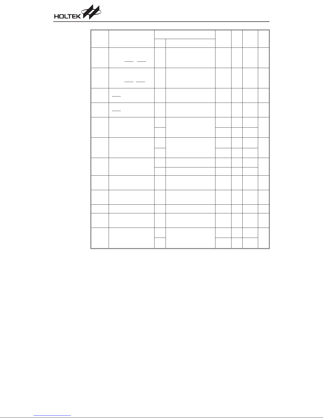
Selection Table
The series of A/D with LCD microcontrollers include a comprehensive range of features, some of
which are standard and some of which are device dependent. Most features are common to all devices, the main features distinguishing them are Program Memory, Data Memory capacity, I/O
count, timer functions, A/D channels, LCD outputs and PWM outputs. To assist users in their selection of the most appropriate device for their application, the following table, which summarizes the
main features of each device, is provided.
Part No.
HT46R62
HT46C62
HT46R63
HT46C63
HT46R64
HT46C64
HT46R65
HT46C65
Note
1. Part numbers including ²C² are mask version devices while ²R² are OTP devices.
2. For devices that exist in two package formats, the table reflects the situation for the larger
package.
Prog.
Data
Mem.
Mem.
2K´14 88´8
4K´15 208´8
4K´15 192´8
8K´16 384´8
I/O LCD Timer Interrupt A/D PWM PFD Buzzer Stack
20´2,
20
32
24
24
20´3or
19´4
20´3or
19´4
33´2,
33´3or
32´4
41´2,
41´3or
40´4
8-bit´1
16-bit´1
8-bit´1
16-bit´1
16-bit´2
6
9-bit´6 8-bit´3 ÖÖ
6
8-bit´8 8-bit´4
7
10-bit´8 8-bit´4 ÖÖ
7
10-bit´8 8-bit´4 ÖÖ
¾¾
6 56SSOP
8
8
16
5
Package
Types
56SSOP,
100QFP
56SSOP,
100QFP
56SSOP,
100QFP
Page 15
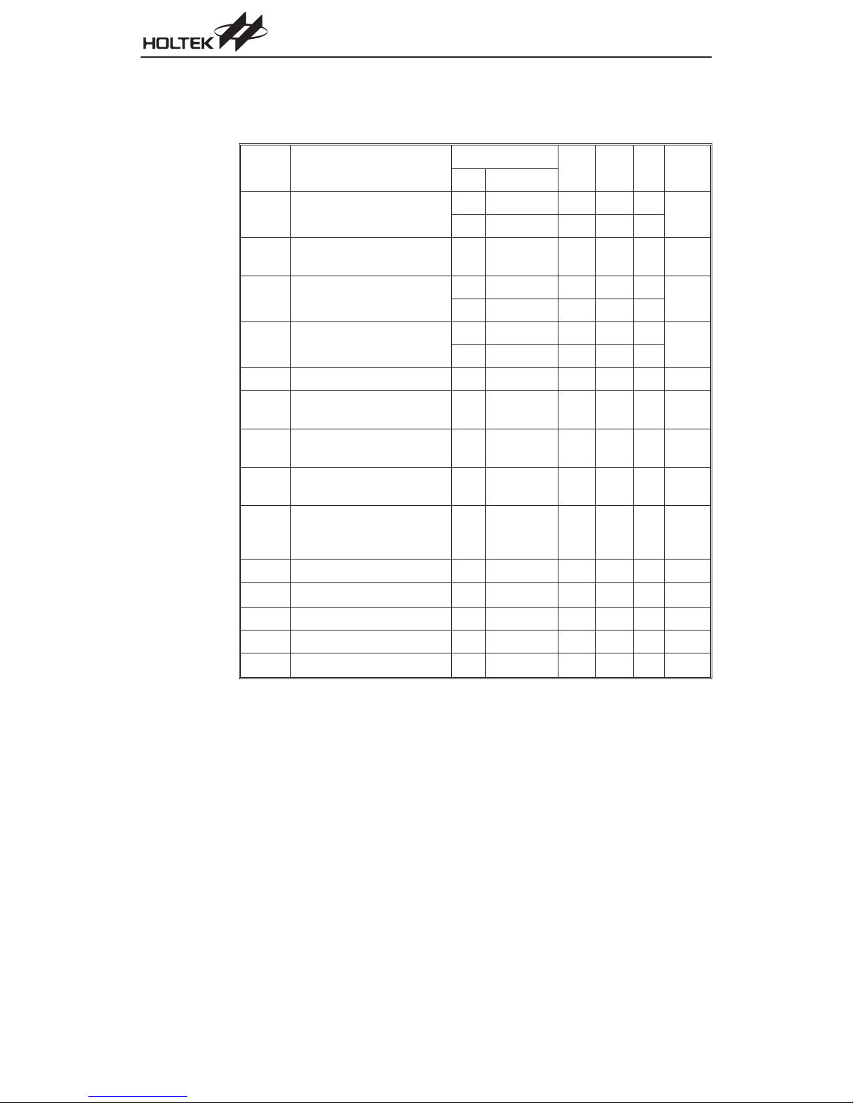
Block Diagram
The following block diagram illustrates the main functional blocks of the A/D with LCD Type
microcontroller series of devices.
A/D with LCD Type MCU
P W M
P r o g r a m
M e m o r y
L o o k - u p
T a b l e
R e g i s t e r
B u z z e r
D r i v e r
A d d r e s s D e c o d e r
L o o k - u p
T a b l e
P o i n t e r
C o n f i g .
R e g i s t e r
S t a c k P o i n t e r
I n t e r r u p t
C i r c u i t
S y s t e m R C /
X ' t a l O s c i l l a t o r
O s c i l l a t o r
L C D D r i v e r s
C O M
R e s e t &
L V R / L V D
1. This block diagram represents the OTP device, for the mask device there is no Device
Note
R T C
O S C
W D T
S E G
C o n v e r t e r
A / D
T i m i n g
G e n e r a t o r
L C D
M e m o r y
D a t a
M e m o r y
C o n f i g .
R e g i s t e r
A d d r e s s D e c o d e r
I n s t r u c t i o n
M
U
X
B a n k
P o i n t e r
W a t c h d o g
T i m e r
D e c o d e r
M e m o r y
P o i n t e r
C o n f i g .
R e g i s t e r
I n s t r u c t i o n
R e g i s t e r
M U X
T i m e r ( s ) /
C o u n t e r
A L U
S h i f t e r
A C C
C o n f i g .
P F D
R e g i s t e r
Programming Circuitry.
2. The Comparator function only exists in the HT46R63/HT46C63 devices.
3. The LVR/LVD, Buzzer driver and PFD do not exist in the HT46R63/HT46C63.
P r o g r a m
C o u n t e r
S t a c k
C o n f i g .
R e g i s t e r
P o r t s
I / O
T o P r o g r a m
M e m o r y
C o m p a r a t o r
C o n f i g u r a t i o n
O p t i o n
D e v ic e
P r o g r a m m i n g
C i r c u i t r y
6
Page 16
Pin Assignment
Chapter 1 Hardware Structure
P A 0 / B Z
1
P A 1 / B Z
2
P A 2
3
P A 3 / P F D
4
P A 4
5
P A 5
6
P A 6
7
P A 7
8
P B 0 / A N 0
9
P B 1 / A N 1
1 0
P B 2 / A N 2
1 1
P B 3 / A N 3
1 2
P B 4 / A N 4
1 3
P B 5 / A N 5
1 4
V S S
1 5
1 6
1 7
1 8
P D 4 / I N T 0
1 9
P D 5 / I N T 1
2 0
P D 6 / T M R
2 1
V L C D
2 2
V M A X
2 3
2 4
V 1
2 5
V 2
2 6
C 1
2 7
C 2
2 8
C O M 0
H T 4 6 R 6 2 / H T 4 6 C 6 2
5 6 S S O P - A
N C
N C
N C
N C
N C
N C
N C
1
2
3
4
5
6
7
8
9
1 0
1 1
1 2
1 3
1 4
1 5
H T 4 6 R 6 3 / H T 4 6 C 6 3
1 6
1 7
1 8
1 9
2 0
2 1
2 2
2 3
2 4
2 5
2 6
2 7
2 8
2 9
3 0
3 1
P C 0
1 0 0 Q F P - A
3 2 3 3 3 4 3 5 3 6 3 7 3 8 3 9 4 0 4 1 4 2 4 3 4 4 4 5 4 6 4 7 4 8 4 9 5 0
P C 6
P C 5
P C 4
P C 3
P C 2
P C 1
P B 0 / A N 0
P B 1 / A N 1
P B 2 / A N 2
P B 3 / A N 3
P B 4 / A N 4
P B 5 / A N 5
P B 6 / A N 6
P B 7 / A N 7
A V D D
N C
N C
N C
N C
P A 0
P A 1
P A 2
P A 3
P A 4
P A 5
P A 6
P A 7
V S S
N C
N C
N C
N C
N C
N C
N C
N C
P D 0 / P W M 0
P D 1 / P W M 1
P D 2 / P W M 2
5 6
5 5
5 4
5 3
5 2
5 1
5 0
4 9
4 8
4 7
4 6
4 5
4 4
4 3
4 2
4 1
4 0
3 9
3 8
3 7
3 6
3 5
3 4
3 3
3 2
3 1
3 0
2 9
R E S
O S C 1
O S C 2
V D D
O S C 3
O S C 4
S E G 0
S E G 1
S E G 2
S E G 3
S E G 4
S E G 5
S E G 6
S E G 7
S E G 8
S E G 9
S E G 1 0
S E G 1 1
S E G 1 2
S E G 1 3
S E G 1 4
S E G 1 5
S E G 1 6
S E G 1 7
S E G 1 8
C O M 3 / S E G 1 9
C O M 2
C O M 1
O S C 4
O S C 3
O S C 2
O S C 1
P B 0 / A N 0
P B 1 / A N 1
P B 2 / A N 2
P B 3 / A N 3
A V D D
P D 0 / P W M 0
P D 1 / P W M 1
P D 2 / P W M 2
P D 3 / P W M 3
V D D
R E S
P A 0
P A 1
P A 2
P A 3
P A 4
P A 5
P A 6
P A 7
V S S
P C 0
P C 1
P C 2
P C 3
H T 4 6 R 6 3 / H T 4 6 C 6 3
C M P O
C H G O
C M P N
C M P P
O S C 4
O S C 3
O S C 2
O S C 1
V D D
R E S
P D 3 / P W M 3
P D 2 / P W M 2
P D 2 / P W M 1
P D 0 / P W M 0
P C 7
V L C D
N C
N C
8 18 28 38 48 58 68 78 88 99 09 19 29 39 49 59 69 79 89 91 0 0
N C
8 0
N C
7 9
N C
7 8
N C
7 7
N C
7 6
N C
7 5
C O M 0
7 4
C O M 1
7 3
C O M 2
7 2
C O M 3 /S E G 1 9
7 1
S E G 1 8
7 0
S E G 1 7
6 9
S E G 1 6
6 8
S E G 1 5
6 7
S E G 1 4
6 6
S E G 1 3
6 5
S E G 1 2
6 4
S E G 1 1
6 3
S E G 1 0
6 2
S E G 9
6 1
S E G 8
6 0
S E G 7
5 9
S E G 6
5 8
S E G 5
5 7
S E G 4
5 6
S E G 3
5 5
S E G 2
5 4
S E G 1
5 3
S E G 0
5 2
N C
5 1
N C
N C
N C
N C
P D 7
P D 6 / T M R
P D 5 / I N T 1
P D 4 / I N T 0
1
2
3
4
5
6
7
8
9
1 0
1 1
1 2
1 3
1 4
1 5
1 6
1 7
1 8
1 9
2 0
2 1
2 2
2 3
2 4
2 5
2 6
2 7
2 8
5 6 S S O P - A
P D 0 / P W M 0
P D 1 / P W M 1
P D 2 / P W M 2
P D 3 / P W M 3
5 6
5 5
5 4
5 3
5 2
5 1
5 0
4 9
4 8
4 7
4 6
4 5
4 4
4 3
4 2
4 1
4 0
3 9
3 8
3 7
3 6
3 5
3 4
3 3
3 2
3 1
3 0
2 9
P B 0 / A N 0
P B 1 / A N 1
P B 2 / A N 2
P B 3 / A N 3
P B 4 / A N 4
P B 5 / A N 5
P B 6 / A N 6
P B 7 / A N 7
P D 4 / I N T 0
P D 5 / I N T 1
P D 6 / T M R 0
P D 7 / T M R 1
C H G O
C M P O
C M P P
C M P N
V L C D
C O M 0
C O M 1
C O M 2
C O M 3 / S E G 1 9
S E G 1 4
S E G 1 3
S E G 1 2
S E G 1 1
S E G 1 0
S E G 9
S E G 8
S E G 7
S E G 6
S E G 5
S E G 4
S E G 3
S E G 2
S E G 1
S E G 0
P D 7
P D 6 / T M R
P D 5 / I N T 1
P D 4 / I N T 0
P A 4
1
P A 5
2
N C
3
N C
4
N C
5
N C
6
N C
7
P A 6
8
P A 7
9
1 0
1 1
1 2
1 3
1 4
1 5
1 6
1 7
V S S
1 8
1 9
2 0
2 1
2 2
2 3
2 4
2 5
2 6
N C
2 7
N C
2 8
N C
2 9
N C
3 0
N C
3 2 3 3 3 4 3 5 3 6 3 7 3 8 3 9 4 0 4 1 4 2 4 3 4 4 4 5 4 6 4 7 4 8 4 9 5 0
3 1
V M A X
V L C D
P D 0 / P W M 0
P D 1 / P W M 1
P D 2 / P W M 2
P D 6 / T M R 0
P A 3 / P F D
P A 1 / B Z
P A 0 / B Z
R E S
P A 2
H T 4 6 R 6 4 / H T 4 6 C 6 4
C 2
C 1
V 2
V 1
P A 0 / B Z
P A 1 / B Z
P A 2
P A 3 / P F D
P A 4
P A 5
P A 6
P A 7
P B 0 / A N 0
P B 1 / A N 1
P B 2 / A N 2
P B 3 / A N 3
P B 4 / A N 4
P B 5 / A N 5
V S S
P D 4 / I N T 0
P D 5 / I N T 1
V L C D
V M A X
V 1
V 2
C 1
C 2
C O M 0
H T 4 6 R 6 4 / H T 4 6 C 6 4
5 6 S S O P - A
O S C 4
O S C 3
O S C 2
O S C 1
V D D
1 0 0 Q F P - A
C O M 2
C O M 1
C O M 0
C O M 3 /S E G 3 2
S E G 3 1
1
2
3
4
5
6
7
8
9
1 0
1 1
1 2
1 3
1 4
1 5
1 6
1 7
1 8
1 9
2 0
2 1
2 2
2 3
2 4
2 5
2 6
2 7
2 8
N C
S E G 3 0
R E S
5 6
O S C 1
5 5
O S C 2
5 4
V D D
5 3
O S C 3
5 2
O S C 4
5 1
S E G 8
5 0
S E G 9
4 9
S E G 1 0
4 8
S E G 1 1
4 7
S E G 1 2
4 6
S E G 1 3
4 5
S E G 1 4
4 4
S E G 1 5
4 3
S E G 1 6
4 2
S E G 1 7
4 1
S E G 1 8
4 0
S E G 1 9
3 9
S E G 2 0
3 8
S E G 2 1
3 7
S E G 2 2
3 6
S E G 2 3
3 5
S E G 2 4
3 4
S E G 2 5
3 3
S E G 2 6
3 2
C O M 3 / S E G 3 2
3 1
C O M 2
3 0
2 9
C O M 1
S E G 0
N C
N C
N C
N C
N C
N C
N C
8 18 28 38 48 58 68 78 88 99 09 19 29 39 49 59 69 79 89 91 0 0
S E G 1
8 0
S E G 2
7 9
S E G 3
7 8
N C
7 7
N C
7 6
N C
7 5
S E G 4
7 4
S E G 5
7 3
S E G 6
7 2
S E G 7
7 1
S E G 8
7 0
S E G 9
6 9
S E G 1 0
6 8
S E G 1 1
6 7
S E G 1 2
6 6
S E G 1 3
6 5
S E G 1 4
6 4
S E G 1 5
6 3
S E G 1 6
6 2
S E G 1 7
6 1
S E G 1 8
6 0
S E G 1 9
5 9
S E G 2 0
5 8
S E G 2 1
5 7
N C
5 6
N C
5 5
N C
5 4
N C
5 3
N C
5 2
N C
S E G 2 9
S E G 2 8
5 1
S E G 2 7
S E G 2 6
S E G 2 5
S E G 2 4
S E G 2 3
S E G 2 2
7
Page 17
P A 0 / B Z
P A 1 / B Z
P A 2
P A 3 / P F D
P A 4
P A 5
P A 6
P A 7
P B 0 / A N 0
P B 1 / A N 1
P B 2 / A N 2
P B 3 / A N 3
P B 4 / A N 4
P B 5 / A N 5
V S S
P D 0 / P W M 0
P D 1 / P W M 1
P D 2 / P W M 2
P D 4 / I N T 0
P D 5 / I N T 1
P D 6 / T M R 0
V L C D
V M A X
V 1
V 2
C 1
C 2
C O M 0
H T 4 6 R 6 5 / H T 4 6 C 6 5
1
2
3
4
5
6
7
8
9
1 0
1 1
1 2
1 3
1 4
1 5
1 6
1 7
1 8
1 9
2 0
2 1
2 2
2 3
2 4
2 5
2 6
2 7
2 8
5 6 S S O P - A
5 6
5 5
5 4
5 3
5 2
5 1
5 0
4 9
4 8
4 7
4 6
4 5
4 4
4 3
4 2
4 1
4 0
3 9
3 8
3 7
3 6
3 5
3 4
3 3
3 2
3 1
3 0
2 9
R E S
O S C 1
O S C 2
V D D
O S C 3
O S C 4
S E G 1 6
S E G 1 7
S E G 1 8
S E G 1 9
S E G 2 0
S E G 2 1
S E G 2 2
S E G 2 3
S E G 2 4
S E G 2 5
S E G 2 6
S E G 2 7
S E G 2 8
S E G 2 9
S E G 3 0
S E G 3 1
S E G 3 2
S E G 3 3
S E G 3 4
C O M 3 / S E G 4 0
C O M 2
C O M 1
P B 0 / A N 0
P B 1 / A N 1
P B 2 / A N 2
P B 3 / A N 3
P B 4 / A N 4
P B 5 / A N 5
P B 6 / A N 6
P B 7 / A N 7
P D 0 / P W M 0
P D 1 / P W M 1
P D 2 / P W M 2
P D 3 / P W M 3
P D 4 / I N T 0
P D 5 / I N T 1
P D 6 / T M R 0
P D 7 / T M R 1
A/D with LCD Type MCU
P A 3 / P F D
P A 1 / B Z
P A 0 / B Z
O S C 3
O S C 2
O S C 1
V D D
R E S
P A 4
P A 2
1
P A 5
2
N C
3
N C
4
N C
5
N C
6
N C
7
P A 6
8
P A 7
9
1 0
1 1
1 2
1 3
1 4
H T 4 6 R 6 5 / H T 4 6 C 6 5
1 5
1 6
1 7
V S S
1 8
1 9
2 0
2 1
2 2
2 3
2 4
2 5
2 6
N C
2 7
N C
2 8
N C
2 9
N C
3 0
N C
3 1
V L C D
1 0 0 Q F P - A
3 2 3 3 3 4 3 5 3 6 3 7 3 8 3 9 4 0 4 1 4 2 4 3 4 4 4 5 4 6 4 7 4 8 4 9 5 0
V 1
V M A X
C O M 2
C O M 1
C O M 0
C 2
C 1
V 2
C O M 3 /S E G 4 0
O S C 4
S E G 0
S E G 1
S E G 2
S E G 3
S E G 4
S E G 5
S E G 6
S E G 7
S E G 8
8 18 28 38 48 58 68 78 88 99 09 19 29 39 49 59 69 79 89 91 0 0
S E G 9
8 0
S E G 1 0
7 9
S E G 1 1
7 8
N C
7 7
N C
7 6
N C
7 5
S E G 1 2
7 4
S E G 1 3
7 3
S E G 1 4
7 2
S E G 1 5
7 1
S E G 1 6
7 0
S E G 1 7
6 9
S E G 1 8
6 8
S E G 1 9
6 7
S E G 2 0
6 6
S E G 2 1
6 5
S E G 2 2
6 4
S E G 2 3
6 3
S E G 2 4
6 2
S E G 2 5
6 1
S E G 2 6
6 0
S E G 2 7
5 9
S E G 2 8
5 8
S E G 2 9
5 7
N C
5 6
N C
5 5
N C
5 4
N C
5 3
N C
5 2
N C
5 1
S E G 3 0
S E G 3 1
S E G 3 2
S E G 3 3
S E G 3 4
S E G 3 5
S E G 3 6
S E G 3 7
S E G 3 8
S E G 3 9
Note The pin compatibility features of the microcontroller packages allow for straightforward upgrading
to devices of higher functionality with minimal changes to application hardware.
8
Page 18
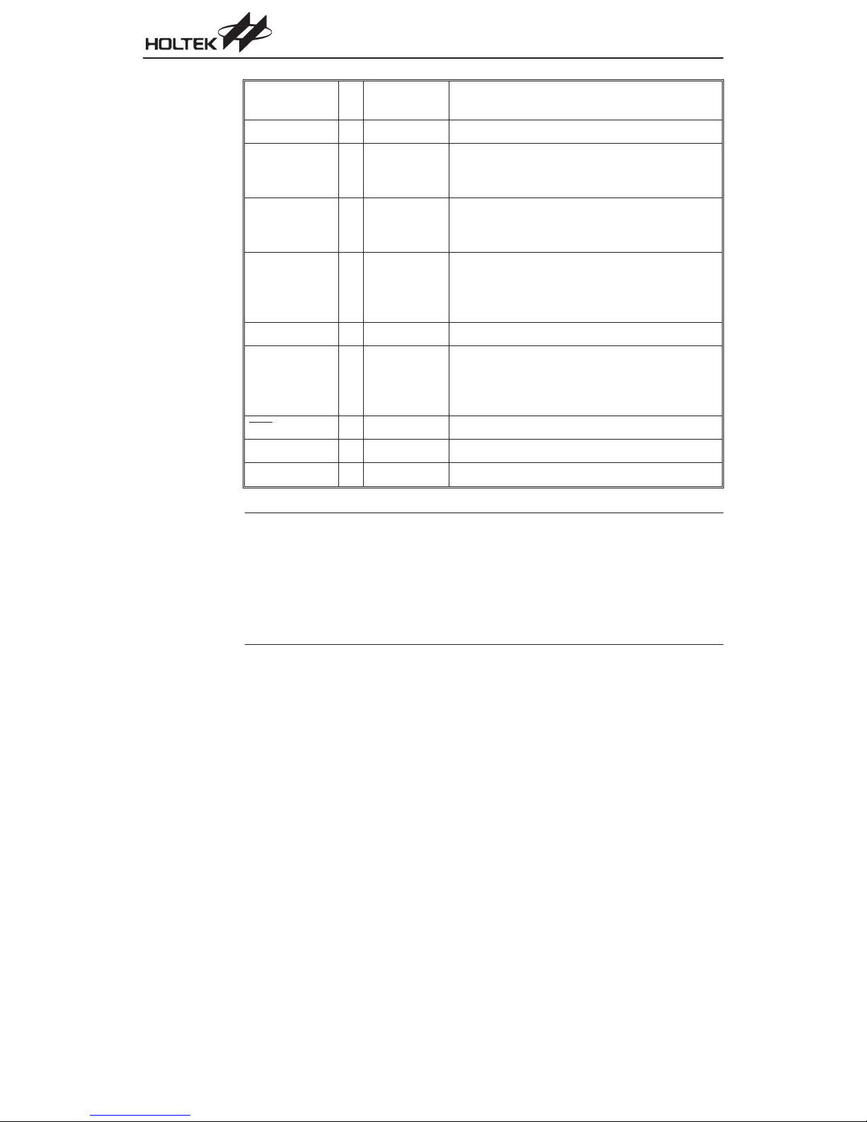
Pin Description
HT46R62/HT46C62
PA0/BZ
PA1/BZ
PA2
PA3/PFD
PA4~PA7
PB0/AN0
PB1/AN1
PB2/AN2
PB3/AN3
PB4/AN4
PB5/AN5
PD0/PWM0
PD1/PWM1
PD2/PWM2
PD4/INT0
PD5/INT1
PD6/TMR
OSC1
OSC2
OSC3
OSC4
VLCD
Pin Name I/O
I/O
I/O Pull-high
I/O
O
O
¾¾
Configuration
Option
Pull-high
Wake-up
Buzzer
PFD
Pull-high
PWM
Interrupt
I
Crystal or RC
I
RTC or
System Clock
Chapter 1 Hardware Structure
Description
Bidirectional 8-bit input/output port. Each individual bit
on this port can be configured as a wake-up input by a
configuration option. Software instructions determine if
the pin is a CMOS output or Schmitt Trigger input. Con
figuration options determine which pins on the port
have pull-high resistors. Pins PA0, PA1 and PA3 are
pin-shared with BZ, BZ
tion of which is chosen via configuration options.
Bidirectional 6-bit input/output port. Software instruc
tions determine if the pin is a CMOS output or Schmitt
Trigger input. Configuration options determine which
pins on the port have pull-high resistors. PB is
pin-shared with the A/D input pins. The A/D inputs are
selected via software instructions. Once selected as an
A/D input, the I/O function and pull-high resistor func
tions are disabled automatically.
Bidirectional 6-bit input/output port. Software instruc
tions determine if the pin is a CMOS output or Schmitt
Trigger input. Configuration options determine which
pins on the port have pull-high resistors. PD0~PD2 are
pin-shared with PWM0~PWM2, the function of each pin
is selected via a configuration option. Pins PD4 and
PD5 are pin-shared with external interrupt input pins
INT0
and INT1 respectively. Configuration options determine the interrupt enable/disable and the interrupt
low/high trigger type. Pin PD6 is pin-shared with the external timer input pin TMR.
OSC1 and OSC2 are connected to an external RC net
work or external crystal (determined by configuration
option) for the internal system clock. For external RC
system clock operation, OSC2 is an output pin for 1/4
system clock. If an RTC oscillator on pins OSC3 and
OSC4 is used as a system clock, then the OSC1 and
OSC2 pins should be left floating.
OSC3 andOSC4 are connected to a 32768Hz crystal to
form a real time clock for timing purposes or to form a
system clock.
LCD power supply
and PFD respectively, the func
-
-
-
-
-
-
9
Page 19
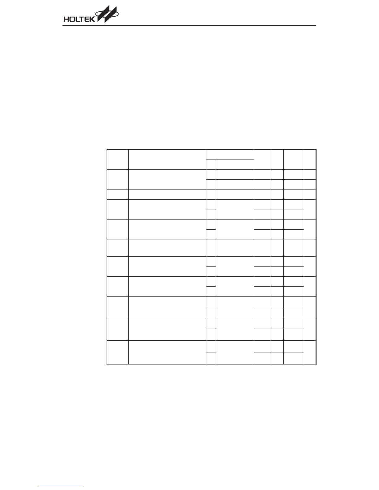
A/D with LCD Type MCU
Pin Name I/O
VMAX
V1, V2, C1, C2 I
SEG0~SEG7 O
SEG8~SEG15 O
SEG16~SEG18 O
COM0~COM2
COM3/SEG19
RES I
VDD
VSS
Note 1. Each pin on Port A can be programmed through a configuration option to have a wake-up
function.
2. Individual pins can be selected to have a pull-high resistor.
Configuration
Option
¾¾
¾
SEG0~SEG7
CMOS Output
SEG8~SEG15
CMOS Output
¾
1/2, 1/3 or 1/4
O
¾¾
¾¾
Duty
¾
Description
IC maximum voltage, connect to VDD,V
LCD voltage pump
LCD driver outputs for LCD panel segments. A configu
ration option can select all pins to be used as segment
drivers or all pins to be used as CMOS outputs.
LCD driveroutputs for LCD panel segments. Configura
tion options can select each pin to be used as either a
segment driver or each pin to be used as a CMOS out
put.
LCD driver outputs for LCD panel segments
An LCD duty-cycle configuration option determines if
SEG19 is configured as a segment driver or as a com
mon output driver for the LCD panel. COM0~COM2 are
the LCD common outputs.
Schmitt Trigger reset input. Active low.
Positive power supply
Negative power supply, ground
LCD
or V1
-
-
-
-
10
Page 20

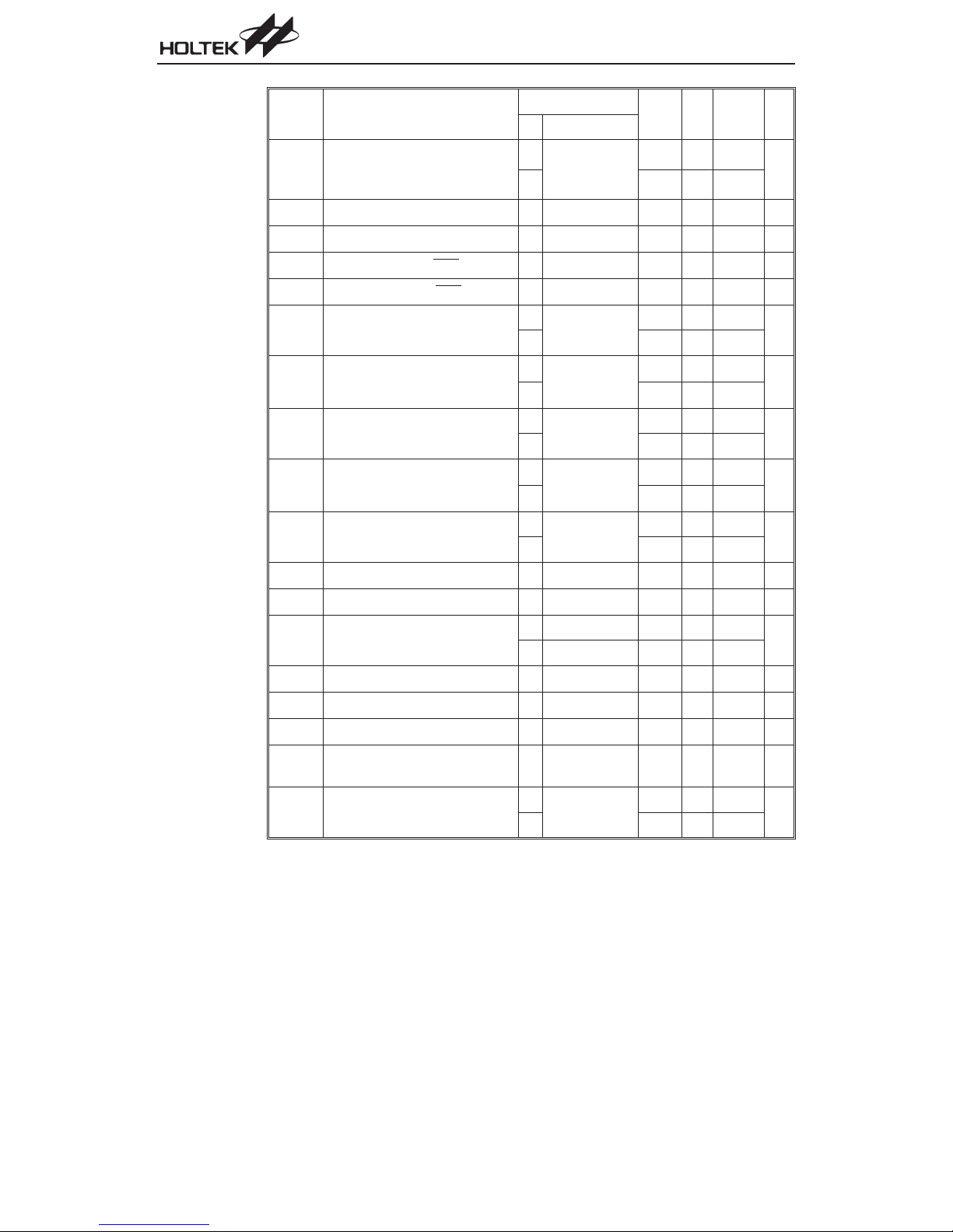
HT46R63/HT46C63
Pin Name I/O
PA0~PA7 I/O
PB0/AN0
PB1/AN1
PB2/AN2
PB3/AN3
PB4/AN4
PB5/AN5
PB6/AN6
PB7/AN7
PC0~PC7 I/O Pull-high
PD0/PWM0
PD1/PWM1
PD2/PWM2
PD3/PWM3
PD4/INT0
PD5/INT1
PD6/TMR
PD7
OSC1
OSC2
OSC3
OSC4
Configuration
Option
Pull-high
Wake-up
I/O Pull-high
Pull-high
I/O
I
O
I
O
PWM
Interrupt
Crystal or RC
¾
Chapter 1 Hardware Structure
Description
Bidirectional 8-bit input/output port. Each individual bit
on this port can be configured as a wake-up input by a
configuration option. Software instructions determine if
the pin is a CMOS output or Schmitt Trigger input. Con
figuration options determine whether the four pins
PA0~PA3 and PA4~PA7 have pull-high resistors. Indi
vidual pins cannot be selected to have pull-high resis
tors.
Bidirectional 8-bit input/output port. Software instruc
tions determine if the pin is a CMOS output or Schmitt
Trigger input. Configuration options determine whether
the four pins PB0~PB3 and PB4~PB7 have pull-high
resistors. Individual pins cannot be selected to have
pull-high resistors. PB is pin-shared with the A/D input
pins. The A/D inputs are selected via software instruc
tions. Once selected as an A/D input, the I/O function
and pull-high resistor functions are disabled automati
cally.
Bidirectional 8-bit input/output port. Software instruc
tions determine if the pin is a CMOS output or Schmitt
Trigger input. Configuration options determine whether
the four pins PC0~PC3 and PC4~PC7 have pull-high
resistors. Individual pins cannot be selected to have
pull-high resistors.
Bidirectional 8-bit input/output port. Software instructions determine if the pin is a CMOS output or Schmitt
Trigger input. Configuration options determine whether
the four pins PD0~PD3 and PD4~PD7 have pull-high
resistors. Individual pins cannot be selected to have
pull-high resistors. PD0~PD3 are pin-shared with
PWM0~PWM3, the function of each pin is selected via
a configuration option. Pins PD4 and PD5 are
pin-shared with external interrupt input pins INT0
INT1
respectively. Configuration options determine the
interrupt enable/disable and the interrupt low/high trig
ger type. Pin PD6 is pin-shared with the external timer
input pin TMR.
OSC1 and OSC2 are connected to an external RC net
work or external crystal (determined by configuration
option) for the internal system clock. For external RC
system clock operation, OSC2 is an output pin for 1/4
system clock.
32768Hz crystal connections for RTC clock generation.
and
-
-
-
-
-
-
-
-
-
11
Page 21
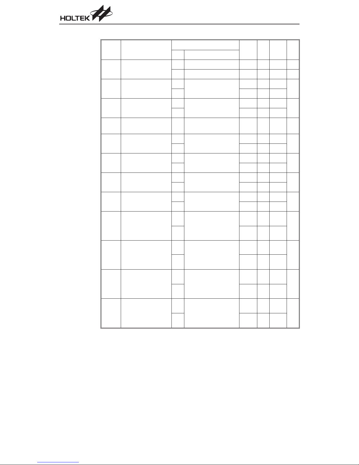
A/D with LCD Type MCU
Pin Name I/O
CMPN I
CMPP I
CMPO O
CHGO O
AVDD
VLCD
SEG0~SEG6 O
SEG7~SEG10 O
SEG11~SEG14 O
SEG15~SEG18 O
COM0~COM2
COM3/SEG19
RES I
VDD
VSS
Configuration
Option
¾
¾
¾
¾
¾¾
¾¾
¾
SEG7~SEG10
CMOS Output
SEG11~SEG14
CMOS Output
SEG15~SEG18
CMOS Output
O 1/3 or 1/4 Duty
¾
¾¾
¾¾
Description
Negative input for comparator
Positive input for comparator
Comparator output
Comparator output with 32768Hz carrier
A/D converter reference voltage input. It should be ex
ternally connected to VDD.
LCD power supply
LCD driver outputs for LCD panel segments.
LCD driver outputs for LCD panel segments. A configu
ration option can select all pins to be used as segment
drivers or all pins to be used as CMOS outputs.
LCD driver outputs for LCD panel segments. A configu
ration option can select all pins to be used as segment
drivers or all pins to be used as CMOS outputs. If used
as CMOS outputs, these pins have a higher sink capa
bility than the SEG7~SEG10 CMOS outputs.
LCD driver outputs for LCD panel segments. A configu
ration option can select all pins to be used as segment
drivers or all pins to be used as CMOS outputs. If used
as CMOS outputs, these pins have a higher sink capa
bility than the SEG7~SEG10 CMOS outputs.
An LCD duty-cycle configuration option determines if
SEG19 is configured as a segment driver or as a common output driver for the LCD panel. COM0~COM2 are
the LCD common outputs.
Schmitt Trigger reset input. Active low.
Positive power supply
Negative power supply, ground
-
-
-
-
-
-
Note 1. Each pin on Port A can be programmed through a configuration option to have a wake-up
function.
2. Individual pins cannot beselected to have a pull-high resistor. Pull-high resistor configuration
options can only be selected in groups of four pins.
3. Pins PB4/AN4 ~ PB7/AN7 only exist on the 100-pin QFP package.
4. Pins PC4~PC7 only exist on the 100-pin QFP package.
5. Segment pins SEG15~SEG18 only exist on the 100-pin QFP package.
6. If the SEG11~SEG18 outputs are configured as CMOS outputs, note that their sink current
capacity is higher than the SEG7~SEG10 outputs.
12
Page 22
HT46R64/HT46C64
Pin Name I/O
PA0/BZ
PA1/BZ
PA2
PA3/PFD
PA4~PA7
PB0/AN0
PB1/AN1
PB2/AN2
PB3/AN3
PB4/AN4
PB5/AN5
PB6/AN6
PB7/AN7
PD0/PWM0
PD1/PWM1
PD2/PWM2
PD3/PWM3
PD4/INT0
PD5/INT1
PD6/TMR0
PD7/TMR1
OSC1
OSC2
OSC3
OSC4
VLCD
VMAX
Configuration
Option
Pull-high
Wake-up
I/O
I/O Pull-high
I/O
Buzzer
PFD
Pull-high
PWM
Interrupt
I
Crystal or RC
O
I
RTC or
O
System Clock
¾¾
¾¾
Chapter 1 Hardware Structure
Description
Bidirectional 8-bit input/output port. Each individual bit
on this port can be configured as a wake-up input by a
configuration option. Software instructions determine
if the pin is a CMOS output or Schmitt Trigger input.
Configuration optionsdetermine which pins on the port
have pull-high resistors. Pins PA0, PA1 and PA3 are
pin-shared with BZ, BZ
function of which is chosen via configuration options.
Bidirectional 8-bit input/output port. Software instruc
tions determine if the pin is a CMOS output or Schmitt
Trigger input. Configuration options determine which
pins on the port have pull-high resistors. PB is
pin-shared with the A/D input pins. The A/D inputs are
selected via software instructions. Once selected as
an A/D input, the I/O function and pull-high resistor
functions are disabled automatically.
Bidirectional 8-bit input/output port. Software instruc
tions determine if the pin is a CMOS output or Schmitt
Trigger input. Configuration options determine which
pins on the porthave pull-highresistors. PD0~PD3 are
pin-shared with PWM0~PWM3, the function of each
pin is selected via a configuration option. Pins PD4
and PD5 are pin-shared with external interrupt input
pins INT0
tions determinethe interrupt enable/disable and the interrupt low/high trigger type. Pins PD6 and PD7 are
pin-shared with the external timer input pins TMR0
and TMR1.
OSC1 andOSC2 are connected to an external RC network or external crystal (determined by configuration
option) for the internal system clock. For external RC
system clock operation, OSC2 is an output pin for 1/4
system clock. If an RTC oscillator on pins OSC3 and
OSC4 is used as a system clock, then the OSC1 and
OSC2 pins should be left floating.
OSC3 and OSC4 are connected to a 32768Hz crystal
to form a real time clock for timing purposes or to form
a system clock.
LCD power supply
IC maximum voltage, connect to VDD,V
and INT1 respectively. Configuration op-
and PFD respectively, the
or V1
LCD
-
-
13
Page 23
A/D with LCD Type MCU
Pin Name I/O
V1, V2, C1, C2 I
SEG0~SEG7 O
SEG8~SEG15 O
SEG16~SEG31 O
COM0~COM2
COM3/SEG32
RES I
VDD
VSS
Note 1. Each pin on Port A can be programmed through a configuration option to have a wake-up
function.
2. Individual pins can be selected to have a pull-high resistor.
3. Pins PB6/AN6 and PB7/AN7 only exist on the 100-pin QFP package.
4. Pin PD3/PWM3 only exists on the 100-pin QFP package.
5. Pin PD7/TMR1 only exists on the 100-pin QFP package. The 56-pin SSOP package has
only one external timer input TMR0.
6. Segment pins SEG0~SEG7 and SEG27~SEG31 only exist on the 100-pin QFP package.
Configuration
Option
¾
SEG0~SEG7
CMOS Output
SEG8~SEG15
CMOS Output
¾
1/2, 1/3 or 1/4
O
¾¾
¾¾
Duty
¾
Description
LCD voltage pump
LCD driver outputs for LCD panel segments. A config
uration option can select all pins to be used as seg
ment drivers or all pins to be used as CMOS outputs.
LCD driver outputs for LCD panel segments. Configu
ration options can select each pin to be used as either
a segment driver or each pin to be used as a CMOS
output.
LCD driver outputs for LCD panel segments
An LCD duty-cycle configuration option determines if
SEG32 is configured as a segment driver or as a com
mon output driver for the LCD panel. COM0~COM2
are the LCD common outputs.
Schmitt Trigger reset input. Active low.
Positive power supply
Negative power supply, ground
-
-
-
-
14
Page 24

HT46R65/HT46C65
Pin Name I/O
PA0/BZ
PA1/BZ
PA2
PA3/PFD
PA4~PA7
PB0/AN0
PB1/AN1
PB2/AN2
PB3/AN3
PB4/AN4
PB5/AN5
PB6/AN6
PB7/AN7
PD0/PWM0
PD1/PWM1
PD2/PWM2
PD3/PWM3
PD4/INT0
PD5/INT1
PD6/TMR0
PD7/TMR1
OSC1
OSC2
OSC3
OSC4
VLCD
VMAX
Configuration
Option
Pull-high
Wake-up
I/O
I/O Pull-high
I/O
¾¾
¾¾
I
Crystal or RC
O
I
O
System Clock
Buzzer
PFD
Pull-high
PWM
Interrupt
RTC or
Chapter 1 Hardware Structure
Description
Bidirectional 8-bit input/output port. Each individual bit
on this port can be configured as a wake-up input by a
configuration option. Software instructions determine
if the pin is a CMOS output or Schmitt Trigger input.
Configuration options determine which pins on the
port have pull-high resistors. Pins PA0, PA1 and PA3
are pin-shared with BZ, BZ
function of which is chosen via configuration options.
Bidirectional 8-bit input/output port. Software instruc
tions determine if the pin is a CMOS output or Schmitt
Trigger input. Configuration options determine which
pins on the port have pull-high resistors. PB is
pin-shared with the A/D input pins. The A/D inputs are
selected via software instructions. Once selected as
an A/D input, the I/O function and pull-high resistor
functions are disabled automatically.
Bidirectional 8-bit input/output port. Software instruc
tions determine if the pin is a CMOS output or Schmitt
Trigger input. Configuration options determine which
pins on the port have pull-high resistors. PD0~PD3
are pin-shared with PWM0~PWM3, the function of
each pin is selected via a configuration option. Pins
PD4 andPD5 are pin-shared with external interrupt input pins INT0
options determinethe interrupt enable/disable and the
interrupt low/high trigger type. Pins PD6 and PD7 are
pin-shared with the external timer input pins TMR0
and TMR1 respectively.
OSC1 and OSC2 are connected to an external RC
network or external crystal (determined by configura
tion option) for the internal system clock. For external
RC system clock operation, OSC2 is an output pin for
1/4 system clock. If an RTC oscillator on pins OSC3
and OSC4 is used as a system clock, then the OSC1
and OSC2 pins should be left floating.
OSC3 and OSC4 are connected to a 32768Hz crystal
to form a real time clock for timing purposes or to form
a system clock.
LCD power supply
IC maximum voltage, connect to VDD,V
and INT1 respectively. Configuration
and PFD respectively, the
or V1
LCD
-
-
-
15
Page 25
A/D with LCD Type MCU
Pin Name I/O
V1, V2, C1, C2 I
SEG0~SEG7 O
SEG8~SEG15 O
SEG16~SEG23 O
SEG24~SEG39 O
COM0~COM2
COM3/SEG40
RES I
VDD
VSS
Configuration
Option
¾
SEG0~SEG7
CMOS output
SEG8~SEG15
CMOS output
SEG16~SEG23
CMOS output
¾
1/2, 1/3 or 1/4
O
¾¾
¾¾
Duty
¾
Description
LCD voltage pump
LCD driver outputs for LCD panel segments. A config
uration option can select all pins to be used as seg
ment driversor all pins to be used asCMOS outputs.
LCD driver outputs for LCD panel segments. A config
uration option can select all pins to be used as seg
ment driversor all pins to be used asCMOS outputs.
LCD driver outputs for LCD panel segments. Configu
ration options can select each pin to be used as either
a segment driver or each pin to be used as a CMOS
output.
LCD driver outputs for LCD panel segments
An LCD duty-cycle configuration option determines if
SEG40 is configured as a segment driver or as a com
mon output driver for the LCD panel. COM0~COM2
are the LCD common outputs.
Schmitt Trigger reset input. Active low.
Positive power supply
Negative power supply, ground
-
-
-
-
-
-
Note 1. Each pin on Port A can be programmed through a configuration option to have a wake-up
function.
2. Individual pins can be selected to have a pull-high resistor.
3. Pins PB6/AN6 and PB7/AN7 only exist on the 100-pin QFP package.
4. Pin PD3/PWM3 only exists on the 100-pin QFP package.
5. Pin PD7/TMR1 only exists on the 100-pin QFP package. The 56-pin SSOP package has
only one external timer input TMR0.
6. Segment pins SEG0~SEG15 and SEG35~SEG39 only exist on the 100-pin QFP package.
16
Page 26
Absolute Maximum Ratings
Supply Voltage.............................................................................................VSS-0.3V to VSS+6.0V
Input Voltage ...............................................................................................V
Storage Temperature.............................................................................................-50°Cto125°C
Operating Temperature............................................................................................-40°Cto85°C
These are stress ratings only. Stresses exceeding the range specified under Absolute Maximum
Ratings may cause substantial damage to the device. Functional operation of this device at other
conditions beyond those listed in the specification is not implied and prolonged exposure to ex
treme conditions may affect device reliability.
D.C. Characteristics
Chapter 1 Hardware Structure
-0.3V to VDD+0.3V
SS
-
For HT46R63/HT46C63
Symbol Parameter
V
V
I
DD1
I
DD2
I
DD3
I
STB1
I
STB2
I
STB3
Operating Voltage
DD
LCD Highest Voltage
LCD
Operating Current (RC OSC,
Analog Circuit Disabled)
Operating Current (RC OSC)
Operating Current
(Crystal OSC, RC OSC)
Standby Current (WDT OSC On,
RTC Off, LCD Off)
Standby Current (WDT OSC Off,
RTC Off, LCD Off)
Standby Current (WDT OSC Off,
RTC On, LCD Off)
Standby Current (WDT OSC Off,
I
STB4
RTC On,LCD On with Low Current
Internal R Type Bias Option)
Standby Current (WDT OSC Off,
I
STB5
RTC On, LCD On with Middle Current Internal R Type Bias Option)
Test Conditions
Conditions
V
DD
¾
f
=4MHz 2.2
SYS
¾
f
=8MHz 3.3
SYS
¾¾
3V
No load,
f
=4MHz
SYS
5V
3V
No load,
f
=4MHz
SYS
5V
No load,
5V
f
=8MHz
SYS
3V
No load,
System HALT
5V
3V
System HALT
5V
3V
System HALT
5V
3V
System HALT
V
LCD=VDD
5V
3V
System HALT
V
LCD=VDD
5V
Ta=25°C
Min. Typ. Max. Unit
¾
5.5 V
¾
5.5 V
¾
0
¾
¾
¾
¾
¾
¾¾
¾¾
¾¾
¾¾
¾¾
¾¾
V
12
DD
V
mA
35
12
mA
35
48mA
5
mA
15
1
mA
1
5
mA
20
10 12 16
mA
20 24 32
16 20 26
mA
32 40 52
17
Page 27
A/D with LCD Type MCU
Symbol Parameter
Standby Current (WDT OSC Off,
I
STB6
RTC On,LCD On with High Current
Internal R Type Bias Option)
V
V
V
V
I
OL1
I
OH1
I
OL2
I
OH2
I
OL3
I
OLTOTAL
I
OHTOTAL
R
V
V
V
E
I
ADC
Input Low Voltage for I/O Ports
IL1
Input High Voltage for I/O Ports
IH1
Input Low Voltage (RES)
IL2
Input High Voltage (RES)
IH2
I/O Port Sink Current
I/O Port Source Current
SEG7~SEG10 Logical Sink
Current
SEG7~SEG18 Logical Source
Current
SEG11~SEG18 Logical Sink
Current
I/O Port Total Sink Current
I/O Port Total Source Current
Pull-high Resistance
PH
Comparator Input Offset Voltage
OS
Comparator Input Voltage Range
1
A/D Input Voltage
AD
A/D Conversion Integral
AD
Nonlinearity Error
Additional Power Consumption
if A/D Converter is used
Test Conditions
Min. Typ. Max. Unit
V
Conditions
DD
3V
System HALT
V
LCD=VDD
5V 76 104 136
V
V
V
V
V
OL
OH
OL
OH
OL
¾
¾
¾
¾
=0.1V
=0.9V
=0.1V
=0.9V
=0.1V
DD
DD
DD
DD
DD
¾
¾
¾
¾
3V
5V 10 25
3V
5V
3V
5V 16
3V
5V
3V
5V 32
¾¾ ¾¾
38 52 68
¾
0
0.7V
0.9V
¾
DD
¾
0
¾
DD
612
-2 -4
-5 -8
¾¾
8
¾¾
-2 -4 ¾
-4 -8 ¾
¾¾
16
¾¾
0.3V
V
0.4V
V
100 mA
¾¾ ¾¾-100
3V
5V
¾
¾
¾
¾
3V
5V
¾
¾
¾
¾
¾
¾¾
¾
20 60 100
10 30 50
-10 ¾
0.2
¾ V
DD
¾
0
V
±0.5 ±1
¾
0.5 1
¾
1.5 3
10 mV
DD
DD
DD
DD
¾
¾
¾
¾
- 0.8
DD
mA
V
V
V
V
mA
mA
mA
mA
mA
mA
kW
V
V
LSB
mA
18
Page 28
Chapter 1 Hardware Structure
For HT46R62/HT46C62, HT46R64/HT46C64, HT46R65/HT46C65
Test Conditions
Symbol Parameter
V
DD
I
DD1
I
DD2
I
DD3
I
DD4
I
STB1
I
STB2
I
STB3
I
STB4
I
STB5
I
STB6
I
STB7
Operating Voltage
Operating Current
(Crystal OSC)
Operating Current
(RC OSC)
Operating Current
(Crystal OSC, RC OSC)
Operating Current
(f
=32768Hz)
SYS
Standby Current
(f
=T1)
S
Standby Current
(f
=32768Hz OSC)
S
Standby Current
(f
=WDT RC OSC)
S
Standby Current
(f
=32768Hz OSC)
S
Standby Current
(f
=32768Hz OSC)
S
Standby Current
(f
=WDT RC OSC)
S
Standby Current
(f
=WDT RC OSC)
S
V
DD
¾
¾
3V
5V
3V
5V
5V
3V
5V
3V
5V
3V
5V
3V
5V
3V
5V
3V
5V
3V
5V
3V
5V
Conditions
f
=4MHz 2.2
SYS
=8MHz 3.3
f
SYS
No load, f
SYS
=4MHz
ADC Off
No load, f
SYS
=4MHz
ADC Off
No load, f
SYS
=8MHz
ADC Off
No load, ADC Off
No load, system HALT
LCD Off
No load, system HALT
LCD On, C type
No load, system HALT
LCD On, C type
No load, system HALT,
LCD On,R type, 1/2 bias,
V
LCD=VDD
(Low bias current option)
No load, system HALT,
LCD On,R type, 1/3 bias,
V
LCD=VDD
(Low bias current option)
No load, system HALT,
LCD On,R type, 1/2 bias,
V
LCD=VDD
(Low bias current option)
No load, system HALT,
LCD On,R type, 1/3 bias,
V
LCD=VDD
(Low bias current option)
Ta=25°C
Min. Typ. Max. Unit
¾
5.5 V
¾
5.5 V
¾
12
¾
35
¾
12
¾
35
¾
48mA
¾
0.3 0.6
¾
0.6 1
¾¾
¾¾
¾
2.5 5
¾
10 20
¾
25
¾
610
¾
17 30
mA
mA
mA
1
mA
2
mA
mA
mA
¾
34 60
¾
13 25
mA
¾
28 50
¾
14 25
mA
¾
26 50
¾
10 20
mA
¾
19 40
19
Page 29
A/D with LCD Type MCU
Symbol Parameter
Input Low Voltage for
V
I/O Ports, TMR, TMR0
IL1
TMR1, INT0
, INT1
Input High Voltage for
V
V
V
I/O Ports, TMR, TMR0
IH1
TMR1, INT0
Input Low Voltage
IL2
(RES
Input High Voltage
IH2
(RES
, INT1
)
)
I/O Port Segment
I
OL
Logic Output Sink
Current
I/O Port Segment
I
OH
Logic Output Source
Current
R
V
V
V
E
Pull-high Resistance
PH
Low Voltage Reset
LVR
Voltage
Low Voltage Detector
LVD
Voltage
A/D Input Voltage
AD
A/D Conversion Inte-
AD
gral Nonlinearity Error
Additional Power
I
ADC
Consumption if A/D
Converter is used
Test Conditions
Min. Typ. Max. Unit
V
DD
¾¾
¾¾
¾¾
¾¾
3V
V
OL
Conditions
=0.1V
DD
0
0.7V
DD
0
0.9V
DD
612
¾
0.3V
¾
¾
0.4V
¾
5V 10 25
3V
V
=0.9V
OH
DD
5V
3V
5V
¾
¾
¾¾
¾¾
¾¾
¾¾ ¾
3V
-2 -4
-5 -8
20 60 100
10 30 50
2.7 3.0 3.3 V
3.0 3.3 3.6 V
¾
0
±0.5 ±1
¾
0.5 1
¾
5V
¾
1.5 3
V
DD
V
V
DD
V
DD
V
V
DD
¾
mA
¾
¾
mA
¾
kW
V
V
DD
LSB
mA
20
Page 30
A.C. Characteristics
Chapter 1 Hardware Structure
For HT46R63/HT46C63
Symbol Parameter
f
SYS
f
RTCOSC
f
TIMER
t
WDTOSC
t
WDT1
t
WDT2
t
WDT3
t
RES
t
SST
t
INT
t
AD
t
ADC
t
ADCS
t
COMP
*t
SYS = 1/fSYS
System Clock
RTC Frequency
(32768Hz Crystal OSC)
Timer Input Frequency
Watchdog Oscillator Period
Watchdog Time-out Period
Watchdog Time-out Period
(f
/4)
SYS
Watchdog Time-out Period
(32768Hz RTC)
External Reset Low Pulse
Width
System Start-up Timer Period
Interrupt Pulse Width
A/D Clock Period
A/D Conversion Time
A/D Sampling Time
Response Time of Comparator
Test Conditions
Min. Typ. Max. Unit
V
Conditions
DD
¾
2.2V~5.5V 400
¾
3.3V~5.5V 400
¾¾¾
¾
2.2V~5.5V 0
¾
3.3V~5.5V 0
3V
5V
¾
¾
¾¾¾¾
¾¾¾¾
¾
4000
¾
8000
32768
¾
4000
¾
8000
45 90 180
32 65 130
216t
2
¾¾¾¾
¾¾
1
¾¾
Power-up or
¾
Wake-up
¾
1024
from HALT
¾¾
¾¾
¾¾
1
1
64
¾¾
¾¾
¾¾
¾¾¾32¾
¾¾¾¾
Ta=25°C
kHz
¾
Hz
kHz
ms
WDTOSC
18
*t
SYS
2s
ms
¾
*t
SYS
ms
ms
t
AD
t
AD
3
ms
21
Page 31

A/D with LCD Type MCU
For HT46R62/HT46C62, HT46R64/HT46C64, HT46R65/HT46C65
Test Conditions
Symbol Parameter
f
SYS1
f
SYS2
f
RTCOSC
f
TIMER
t
WDTOSC
t
WDT1
t
WDT2
t
WDT3
t
RES
t
SST
t
LVR
t
INT
t
AD
t
ADC
t
ADCS
*t
SYS
System Clock
System Clock
(32768Hz Crystal OSC)
RTC Frequency
Timer I/P Frequency
(TMR0/TMR1)
Watchdog Oscillator
Period
Watchdog Time-out
Period (
WDT
OSC)
Watchdog Time-out
Period (f
SYS
/4)
Watchdog Time-out
Period (32768Hz
External Reset Low
Pulse Width
System Start-up Timer
Period
Low Voltage Width to
Reset
Interrupt Pulse Width
A/D Clock Period 5V
A/D Conversion Time
A/D Sampling Time
= 1/f
SYS1
or 1/f
SYS2
V
DD
¾
¾
¾¾ ¾
¾¾ ¾
¾
¾
3V
5V
¾¾
¾¾
¾¾
)
RTC
¾¾
¾
¾¾
¾¾
¾¾ ¾76¾
¾¾ ¾32¾
Conditions
2.2V~5.5V 400
3.3V~5.5V 400
2.2V~5.5V 0
3.3V~5.5V 0
¾
¾
Power-up or Wake-up
from HALT
¾
Ta=25°C
Min. Typ. Max. Unit
¾
4000 kHz
¾
8000 kHz
32768
32768
45 90 180
32 65 130
15
2
17
2
1
1
¾
1
1
1
¾
¾
¾
4000 kHz
¾
8000 kHz
16
¾
2
18
¾
2
¾
2s
¾¾
¾
1024
¾¾
¾¾
¾¾
Hz
Hz
ms
ms
t
WDTOSC
*t
SYS
ms
*t
SYS
ms
ms
ms
t
AD
t
AD
22
Page 32
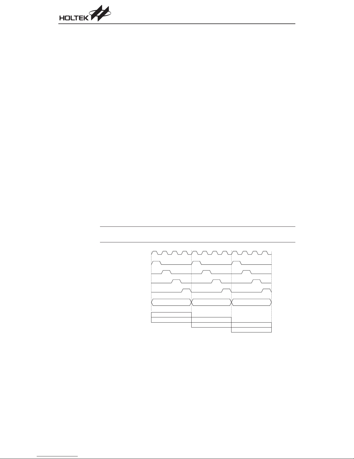
System Architecture
A key factor in the high performance features of the Holtek range of A/D with LCD Type
microcontrollers is attributed to the internal system architecture. The range of devices take advan
tage of the usual features found within RISC microcontrollers providing increased speed of opera
tion and enhanced performance. The pipelining scheme is implemented in such a way that
instruction fetching and instruction execution are overlapped, hence instructions are effectively ex
ecuted in one cycle, with the exception of branch or call instructions. An 8-bit wide ALU is used in
practically all operations of the instruction set. It carries out arithmetic operations, logic operations,
rotation, increment, decrement, branch decisions, etc. The internal data path is simplified by mov
ing data through the Accumulator and the ALU. Certain internal registers are implemented in the
Data Memory and can be directly or indirectly addressed. The simple addressing methods of
these registers along with additional architectural features ensure that a minimum of external com
ponents is required to provide a functional I/O, A/D and LCD control system with maximum reliabil
ity and flexibility. This makes these devices suitable for low cost, high-volume production for
controller applications requiring from 2K up to 8K words of program memory and from 88 to 384
bytes of data storage.
Clocking and Pipelining
The mainsystem clock, derived from either a Crystal/Resonator or RC oscillator issubdivided into
four internally generated non-overlapping clocks, T1~T4. The Program Counter is incremented at
the beginning of the T1 clock during which time a new instruction is fetched. The remaining T2~T4
clocks carry out the decoding and execution functions. In this way, one T1~T4 clock cycle forms
one instruction cycle. Although the fetching and execution of instructions takes place in consecu
tive instruction cycles, the pipelining structure of the microcontroller ensures that instructions are
effectively executed in one instruction cycle. The exception to this are instructions where the contents of the Program Counter are changed, such as subroutine calls or jumps, in which case the instruction will take one more instruction cycle to execute.
Chapter 1 Hardware Structure
-
-
-
-
-
-
-
Note
When the RC oscillator is used, OSC2 is freed for use as a T1 phase clock synchronizing pin. This
T1 phase clock has a frequency of f
O s c i l l a t o r C l o c k
( S y s t e m C l o c k )
P h a s e C l o c k T 1
P h a s e C l o c k T 2
P h a s e C l o c k T 3
P h a s e C l o c k T 4
P r o g r a m C o u n t e r
P i p e l i n i n g
F e t c h I n s t . ( P C )
E x e c u t e I n s t . ( P C - 1 )
/4 with a 1:3 high/low duty cycle.
SYS
P C P C + 1 P C + 2
F e t c h I n s t . ( P C + 1 )
E x e c u t e I n s t . ( P C )
F e t c h I n s t . ( P C + 2 )
E x e c u t e I n s t . ( P C + 1 )
System Clocking and Pipelining
23
Page 33

A/D with LCD Type MCU
For instructions involving branches, such as jump or call instructions, two machine cycles are re
quired to complete instruction execution. An extra cycle is required as the program takes one cy
cle to first obtain the actual jump or call address and then another cycle to actually execute the
branch. The requirement for this extra cycle should be taken into account by programmers in tim
ing sensitive applications
1
2
3
4
5
6
D E L A Y :
M O V A , [ 1 2 H ]
C A L L D E L A Y
C P L [ 1 2 H ]
:
:
N O P
F e t c h I n s t . 1 E x e c u t e I n s t . 1
F e t c h I n s t . 2
E x e c u t e I n s t . 2
F e t c h I n s t . 3
F l u s h P i p e l i n e
F e t c h I n s t . 6 E x e c u t e I n s t . 6
F e t c h I n s t . 7
Program Counter
During program execution, the Program Counter is used to keep track of the address of the next in
struction to be executed. It is automatically incremented by one each time an instruction is exe
cuted except for instructions such as JMP or CALL that demand a jump to a non-consecutive
Program Memory address. For the A/D with LCD series of microcontrollers, note that the Program
Counter width varies with the Program Memory capacity depending upon which device is se
lected. However, it must be noted that only the lower 8 bits, known as the Program Counter Low
Register, are directly addressable by the user.
When executing instructions requiring jumps to non-consecutive addresses such as a jump in
struction, a subroutine call, interrupt or reset, etc., the microcontroller manages program control
by loading the required address into the Program Counter. For conditional skip instructions, once
the condition has been met, the next instruction, which has already been fetched during the present instruction execution, is discarded and a dummy cycle takes its place while the correct instruction is obtained.
-
-
-
-
-
-
-
The lower byte of the Program Counter, known as the Program Counter Low register or PCL, is
available for program control and is a readable and writable register. By transferring data directly
into this register, a short program jump can be executed directly, however, as only this low byte is
available for manipulation, the jumps are limited to the present page of memory, that is 256 locations. When such program jumps are executed it should also be noted that a dummy cycle will be
inserted.
Note
The lower byte of the Program Counter is fully accessible under program control. The use of the
PCL might cause program branching, so an extra cycle is needed to pre-fetch. Further information
on the PCL register can be found in the Special Function Register section.
24
Page 34

Chapter 1 Hardware Structure
Mode
Initial Reset 0 0 0 0000000000
External Interrupt 0 0 0 0 0000000100
External Interrupt 1 0 0 0 0000001000
Timer/Event Counter 0 Overflow 0 0 0 0000001100
Timer/Event Counter 1 Overflow 0 0 0 0000010000
Time Base Interrupt
(HT46R63/HT46C63 only)
Time Base Interrupt
(except HT46R63/HT46C63)
A/D Converter Interrupt
(HT46R63/HT46C63 only)
RTC Interrupt 0 0 0 0000011000
A/D Converter Interrupt
(except HT46R63/HT46C63)
Skip Program Counter + 2
Loading PCL PC12 PC11 PC10 PC9 PC8 @7 @6 @5 @4 @3 @2 @1 @0
Jump, Call Branch #12 #11 #10 #9 #8 #7 #6 #5 #4 #3 #2 #1 #0
Return from Subroutine S12 S11 S10 S9 S8 S7 S6 S5 S4 S3 S2 S1 S0
b12 b11 b10 b9 b8 b7 b6 b5 b4 b3 b2 b1 b0
0 0 0 0000010000
0 0 0 0000010100
0 0 0 0000010100
0 0 0 0000011100
Program Counter Bits
Note 1. PC12~PC8: Current Program Counter bits
2. @7~@0: PCL bits
3. #12~#0: Instruction code bits
4. S12~S0: Stack register bits
5. For the HT46R65/HT46C65, the Program Counter is 13 bits wide, i.e. from b12~b0.
6. For the HT46R63/HT46C63 and HT46R64/HT46C64, since their Program Counter is 12 bits
wide, the b12 column in the table is not applicable.
7. For the HT46R62/HT46C62, since its Program Counter is 11 bits wide, the b11 and b12 columns in the table are not applicable.
8. The Timer/Event Counter 1 Overflow row is available only for the HT46R64/HT46C64 and
HT46R65/HT46C65.
9. For the HT46R62/HT46C62 and HT46R63/HT46C63, the Timer/Event Counter represents
the single timer, known as TMR.
Stack
This is a special part of the memory which is used to save the contents of the Program Counter
only.The stack can have between 6, 8 or 16 levels dependingupon which device is selected and is
neither partof the data nor part of the program space, and is neither readable nor writable. The acti
vated level is indexed by the stack pointer (SP) and is neither readable nor writable. At a subrou
tine call or interrupt acknowledge signal, the contents of theProgram Counterare pushedonto the
stack. At the end of a subroutine or an interrupt routine, signaled by a return instruction (RET or
RETI), the Program Counter is restored to its previous value from the stack. After a chip reset, the
SP will point to the top of the stack.
25
-
-
Page 35

A/D with LCD Type MCU
If the stack is full and an enabled interrupt takes place, the interrupt request flag will be recorded
but the acknowledge signal will be inhibited. When the stack pointer is decremented (by RET or
RETI), the interrupt will be serviced. This feature prevents stack overflow allowing the program
mer to use the structure more easily. However, when the stack is full, a CALL subroutine instruc
tion can still beexecuted whichwill result in a stack overflow. Precautions should be taken to avoid
such cases which might cause unpredictable program branching.
P r o g r a m C o u n t e r
-
-
T o p o f S T A C K
S t a c k
P o i n t e r
B o t t o m o f S T A C K
1. For the HT46R62/HT46C62, N=6, i.e. 6 levels of stack available.
Note
S t a c k L e v e l 1
S t a c k L e v e l 2
S t a c k L e v e l 3
S t a c k L e v e l N
P r o g r a m
M e m o r y
2. For the HT46R63/HT46C63 and HT46R64/HT46C64, N=8, i.e. 8 levels of stack available.
3. For the HT46R65/HT46C65, N=16, i.e. 16 levels of stack available.
Arithmetic and Logic Unit - ALU
The arithmetic-logic unit or ALU is a critical area of the microcontroller that carries out arithmetic
and logic operations of the instruction set. Connected to the main microcontroller data bus, the
ALU receives related instruction codes and performs the required arithmetic or logical operations
after which the result will be placed in the specified register. As these ALU calculation or operations may result in carry, borrow or other status changes, the status register will be correspondingly updated to reflect these changes. The ALU supports the following functions:
· Arithmetic operations ADD, ADDM, ADC, ADCM, SUB, SUBM, SBC, SBCM, DAA
· Logic operations AND, OR, XOR, ANDM, ORM, XORM, CPL, CPLA
· Rotation RRA, RR, RRCA, RRC, RLA, RL, RLCA, RLC
·
Increment and Decrement INCA, INC, DECA, DEC
·
Branch decision, JMP, SZ, SZA, SNZ, SIZ, SDZ, SIZA, SDZA, CALL, RET, RETI
26
Page 36

Program Memory
The Program Memory is the location where the user code or program is stored. For
microcontrollers, two types of Program Memory are usually supplied. The first type is the OneTime Programmable (OTP) Memory where users can program their application code into the de
vice. Devices with OTP memory are denoted by having an ²R² within their device name. By using
the appropriate programming tools, OTP devices offer users the flexibility to freely develop their
applications which may be useful during debug or for products requiring frequent upgrades or pro
gram changes. OTP devices are also applicable for use in applications that require low or medium
volume production runs. The other type of memory is the mask ROM memory, denoted by having
a ²C²within the device name. These devices offer the most cost effective solutions for high volume
products.
Organization
The Program Memory has a capacity of 2K by 14 to 8K by 16 bits depending upon which device is
selected. The Program Memory is addressed by the Program Counter and also contains data, ta
ble information and interrupt entries. Table data, which can be setup in any location within the Pro
gram Memory, is addressed by a separate table pointer register.
Chapter 1 Hardware Structure
-
-
-
-
The following diagram shows the Program Memory for the A/D with LCD Type
0 0 0 H
0 0 4 H
0 0 8 H
0 0 C H
0 1 0 H
0 1 4 H
0 1 8 H
0 1 C H
7 F F H
8 0 0 H
F F F H
1 0 0 0 H
1 F F F H
H T 4 6 R 6 2
H T 4 6 C 6 2
I n i t i a l i z a t i o n
V e c t o r
E x t e r n a l I N T 0
I n t e r r u p t V e c t o r
E x t e r n a l I N T 1
I n t e r r u p t V e c t o r
T i m e r / C o u n t e r
I n t e r r u p t V e c t o r
T i m e B a s e
I n t e r r u p t V e c t o r
R T C I n t e r r u p t
V e c t o r
A / D C o n v e r t e r
I n t e r r u p t V e c t o r
H T 4 6 R 6 3
H T 4 6 C 6 3
I n i t i a l i z a t i o n
V e c t o r
E x t e r n a l I N T 0
I n t e r r u p t V e c t o r
E x t e r n a l I N T 1
I n t e r r u p t V e c t o r
T i m e r / C o u n t e r
I n t e r r u p t V e c t o r
T i m e B a s e
I n t e r r u p t V e c t o r
A / D C o n v e r t e r
I n t e r r u p t V e c t o r
R T C I n t e r r u p t
V e c t o r
1 5 b i t s1 4 b i t s
H T 4 6 R 6 4
H T 4 6 C 6 4
I n i t i a l i z a t i o n
V e c t o r
E x t e r n a l I N T 0
I n t e r r u p t V e c t o r
E x t e r n a l I N T 1
I n t e r r u p t V e c t o r
T i m e r / C o u n t e r 0
I n t e r r u p t V e c t o r
T i m e r / C o u n t e r 1
I n t e r r u p t V e c t o r
T i m e B a s e
I n t e r r u p t V e c t o r
R T C i n t e r r u p t
V e c t o r
A / D C o n v e r t e r
I n t e r r u p t V e c t o r
H T 4 6 R 6 5
H T 4 6 C 6 5
I n i t i a l i z a t i o n
V e c t o r
E x t e r n a l I N T 0
I n t e r r u p t V e c t o r
E x t e r n a l I N T 1
I n t e r r u p t V e c t o r
T i m e r / C o u n t e r 0
I n t e r r u p t V e c t o r
T i m e r / C o u n t e r 1
I n t e r r u p t V e c t o r
T i m e B a s e
I n t e r r u p t V e c t o r
R T C i n t e r r u p t
V e c t o r
A / D C o n v e r t e r
I n t e r r u p t V e c t o r
1 6 b i t s1 5 b i t s
MCU
N o t I m p l e m e n t e d
series.
27
Page 37

Special Vectors
A/D with LCD Type MCU
Within the Program Memory, certain locations are reserved for special usage such as reset and in
terrupts.
Location 000H
·
This vector is reserved for use by the chip reset for program initialization. After a chip reset is ini
tiated, the program will jump to this location and begin execution.
Location 004H
·
This vector is used by the external interrupt INT0
low, the program will jump to this location and begin execution if the external interrupt is enabled
and the stack is not full.
Location 008H
·
This vector is used by the external interrupt INT1
low, the program will jump to this location and begin execution if the external interrupt is enabled
and the stack is not full.
Location 00CH
·
This internal vector is used by the Timer/Event Counter. If a counter overflow occurs, the pro
gram will jump to this location and begin execution if the timer interrupt is enabled and the stack
is not full. For the HT46R64/HT46C64 and HT46R65/HT46C65 devices, which have dual tim
ers, this timer is known as Timer/Event Counter 0 or TMR0, for the other devices the timer is
known as TMR.
Location 010H
·
For the HT46R63/46C63 devices, this internal vector is reserved for use by the Time Base Inter
rupt. When a Time Base Interrupt signal is generated, the program will jump to this location and
begin execution if the interrupt is enabled and the stack is not full. For the HT46R64/HT46C64
and HT46R65/HT46C65 devices, this internal vector is used by the Timer/Event Counter 1. If a
TMR1 counter overflow occurs, the program will jump to this location and begin execution if the
internal interrupt is enabled and the stack is not full. Note that the HT46R62/HT46C62 devices
have only one timer, this interrupt vector is therefore not used.
· Location 014H
For the HT46R63/HT46C63 devices, this internal vector is used by the A/D converter. When an
A/D conversion cycle is complete, the program will jump to this location and begin execution if
the A/D interrupt is enabled and the stack is not full. For the HT46R62/HT46C62, HT46R64/
HT46C64 andHT46R65/HT46C65 devices, this internal vector is reserved for theTime Base Interrupt. When a Time Base Interrupt signal is generated, the program will jump to this location
and begin execution if the interrupt is enabled and the stack is not full.
·
Location 018H
This internal vector is used by the Real Time Clock Interrupt. The program will jump to this loca
tion and begin execution when a Real Time Clock Interrupt signal is generated if the interrupt is
enabled and the stack is not full.
·
Location 01CH
This vector, only available for the HT46R62/HT46C62, HT46R64/HT46C64 and HT46R65/
HT46C65 devices, is used by the A/D converter interrupt. When an A/D conversion cycle is
complete, the program will jump to this location and begin execution if the A/D interrupt is en
abled and the stack is not full.
. If the external interrupt pin on the device goes
. If the external interrupt pin on the device goes
-
-
-
-
-
-
-
28
Page 38

Chapter 1 Hardware Structure
Look-up Table
Any location within the Program Memory can be defined as a look-up table where programmers
can store fixed data. To use the look-up table, the table pointer must first be setup by placing the
lower-order address of the look-up data to be retrieved in the Table Pointer Register TBLP. This
register defines the lower 8-bit address of the look-up table. After setting up the table pointer, the
table data can be retrieved from the current Program Memory page or last Program Memory page
using the ²TABRDC [m]² or ²TABRDL [m]² instructions respectively. When these instructions are
executed, the lower order table byte from the Program Memory will be transferred to the user de
fined Data Memory register [m] as specified in the instruction. The higher order table data byte
from the Program Memory will be transferred to the TBLH special register. Any unused bits in this
transferred higher order byte will be read as ²0².
The following diagram illustrates the addressing/data flow of the look-up table:
P r o g r a m C o u n t e r
h i g h b y t e
T B L P
T B L H S p e c i f i e d b y [ m ]
H i g h b y t e o f t a b l e c o n t e n t s
P r o g r a m
M e m o r y
L o w b y t e o f t a b l e c o n t e n t s
-
Table Program Example
The following example shows how the table pointer and table data is defined and retrieved from
the HT46R63 A/D with LCD microcontroller. This example uses raw table data located in the last
page which is stored there using the ORG statement. The value at this ORG statement is ²F00²
hex which refers to the start address of the last page within the 4K Program Memory of the
HT46R63 microcontroller. The table pointer is setup here to have an initial value of 06 hex.
This will ensure that the first data read from the data table will be at the Program Memory address
F06 hex or 6 locations after the start of the last page. Note that the value for the table pointer is referenced to the first address of the present page if the ²TABRDC [m]² instruction is being used. The
high byte of the table data which in this case is equal to zero will be transferred to the TBLH register automatically when the ²TABRDL [m]² instruction is executed.
tempreg1 db ? ; temporary register #1
tempreg2 db ? ; temporary register #2
:
:
mov a,06h ; initialize table pointer - note that this address
mov tblp,a ; to the last page or present page
:
:
tabrdl tempreg1 ; transfers value in table referenced by table pointer
; is referenced
; to tempregl
; data at prog. memory address F06H transferred to
; tempreg1 and TBLH
29
Page 39

A/D with LCD Type MCU
dec tblp ; reduce value of table pointer by one
tabrdl tempreg2 ; transfers value in table referenced by table pointer
:
:
org F00h ; sets initial address of last page (for HT46R63)
dc 00Ah, 00Bh, 00Ch, 00Dh, 00Eh, 00Fh, 01Ah, 01Bh
:
:
Because the TBLH register is a read-only register and cannot be restored, care should be taken to
ensure its protection if both the main routine and Interrupt Service Routine use table read instruc
tions. If using the table read instructions, the Interrupt Service Routines may change the value of
the TBLH and subsequently cause errors if used again by the main routine. As a rule it is recom
mended that simultaneous useof thetable read instructions should be avoided. However, in situa
tions where simultaneous use cannot be avoided, the interrupts should be disabled prior to the
execution of any main routine table-read instructions. Note that all table related instructions re
quire two instruction cycles to complete their operation.
Instruction
TABRDC [m] PC12 PC11 PC10 PC9 PC8 @7 @6 @5 @4 @3 @2 @1 @0
TABRDL [m] 11111@7@6@5@4@3@2@1@0
b12 b11 b10 b9 b8 b7 b6 b5 b4 b3 b2 b1 b0
; to tempreg2
; data at prog. memory address F05H transferred to
; tempreg2 and TBLH
; in this example the data ²1A² is transferred to
; tempreg1 and data ²0F² to register tempreg2
; the value ²0² will be transferred to the high byte
; register TBLH
Table Location Bits
-
-
-
-
Note 1. PC12~PC8: Current Program Counter bits
2. @7~@0: Table Pointer TBLP bits
3. For the HT46R65/HT46C65, the Table address location is 13 bits, i.e. from b12~b0.
4. For the HT46R63/HT46C63 and HT46R64/HT46C64, the Table address location is 12 bits,
i.e. from b11~b0.
5. For the HT46R62/HT46C62, the Table address location is 11 bits, i.e. from b10~b0.
30
Page 40

Data Memory
Chapter 1 Hardware Structure
The Data Memory is a volatile area of 8-bit wide RAM internal memory and is the location where
temporary information is stored. Divided into three sections, the first of these is an area of RAM
where special function registers are located. These registers have fixed locations and are neces
sary for correct operation of the device. Many of these registers can be read from and written to di
rectly under program control, however, some remain protected from user manipulation. The
second area of Data Memory is reserved for general purpose use. All locations within this area are
read and write accessible under program control. For the HT46R65/HT46C65 devices, this Gen
eral Purpose Data Memory is divided into two individual areas which are two banks known as
Bank 0 and Bank 2, the required area or bank is selected by setting the Bank Pointer to the correct
value. The third area is reserved for the LCD Memory. This special area of Data Memory is
mapped directly to the LCD display so data written into this memory area will directly affect the dis
played data. The addresses of the LCD Memory area overlap those in the General Purpose data
memory area, switching between the two areas is achieved by setting the Bank Pointer to the cor
rect value.
Organization
The Special Purpose and General Purpose Data Memory are located at consecutive locations. All
are implemented in RAM and are 8 bits wide, but the length of each memory section is dictated by
the type of microcontroller chosen. The start address of the Data Memory for all devices is the ad
dress 00H. Registers which are common to all microcontrollers, such as ACC, PCL, etc., have the
same Data Memory address. The LCD data memory is mapped into Bank 1 of the Data Memory,
however, only the lower four bits are used. The higher four bits, if read by the program will return a
²0² value. The start of LCD Data Memory for all devices is the address 40H. However, since the
LCD Data Memory is located in Bank 1, to access this area the Bank Pointer must first be set to a
value of²01H². Note that after power-on, the contents of the Data Memory, including the LCD Data
Memory, will be in an unknown condition, the programmer must therefore ensure that the Data
Memory is properly initialized.
-
-
-
-
-
-
0 0 H
S p e c i a l P u r p o s e
D a t a M e m o r y
2 7 H / 2 F H / 3 F H
2 8 H / 3 0 H / 4 0 H
G e n e r a l P u r p o s e D a t a M e m o r y
C a p a c i t y i s D e v i c e D e p e n d e n t
Note
Most of the Data Memory bits can be directly manipulated using the ²SET [m].² and ²CLR [m].i²
B a n k 0
7 F H / F F H
B a n k 0
B a n k 1
B a n k 2
B a n k 1
L C D M e m o r y
C a p a c i t y i s D e v i c e D e p e n d e n t
B a n k 2
G e n e r a l P u r p o s e D a t a M e m o r y
( H T 4 6 R 6 5 / H T 4 6 C 6 5 d e v i c e s o n l y )
with the exception of a few dedicated bits. The Data Memory can also be accessed through the
memory pointer registers MP0 and MP1.
31
Page 41

A/D with LCD Type MCU
General Purpose Data Memory
All microcontroller programs require an area of read/write memory where temporary data can be
stored and retrieved for use later. It is this area of RAM memory that is known as General Purpose
Data Memory. This area of Data Memory is fully accessible by the user program for both read and
write operations. By using the ²SET[m].i² and ²CLR [m].i² instructions, individual bits can be set or
reset under program control, giving the user a large range of flexibility for bit manipulation in the
Data Memory. As the General Purpose Data Memory exists in Bank 0 for the HT46R62/HT46C62,
HT46R63/HT46C63 and HT46R64/HT46C64 devices and in Bank 0 and Bank 2 for the
HT46R65/HT46C65 devices, it is necessary to first ensure that the Bank Pointer is properly set to
the correct value before accessing the General Purpose Data Memory. When the Bank Pointer is
set to the value ²01H², the LCD Memory will be accessed. Bank 1 or Bank 2 must be addressed in
directly using the memory pointer MP1 and the indirect addressing register IAR1. Any direct ad
dressing or any indirect addressing using MP0 and IAR0 will always result in data from Bank 0
being accessed.
The following diagram shows the General Purpose Data Memory Organization Map for the A/D
with LCD Type microcontrollers:
-
-
H T 4 6 R 6 2
H T 4 6 C 6 2
2 8 H
4 0 H
B a n k 0
7 F H
8 8 B y t e s
The 384 bytes of General Purpose Data Memory in the HT46R65/HT46C65 devices are stored in
Note
H T 4 6 R 6 3
H T 4 6 C 6 3
3 0 H
4 0 H
8 0 H
B a n k 0
F F H
2 0 8 B y t e s
H T 4 6 R 6 4
H T 4 6 C 6 4
4 0 H
6 0 H
8 0 H
B a n k 0
F F H
H T 4 6 R 6 5
H T 4 6 C 6 5
4 0 H
6 0 H
8 0 H
B a n k 0
F F H
B a n k 2
3 8 4 B y t e s1 9 2 B y t e s
two individual memory banks, known as Bank 0 and Bank 2. Before reading or writing to the Gen
eral Purpose Data Memory it is essential to first ensure that the correct Data Memory bank is se
lected by setting up the Bank Pointer. Bank 2 can only be addressed indirectly using MP1 and
IAR1.
Special Purpose Data Memory
This area of Data Memory is where registers, necessary for the correct operation of the
microcontroller, are stored. Most of the registers are both readable and writable but some are pro
tected and are readable only, the details of which are located under the relevant Special Function
Register section. Note that for locations that are unused, any read instruction to these addresses
will return the value ²00H².
G e n e r a l P u r p o s e
D a t a M e m o r y
-
-
-
32
Page 42

Chapter 1 Hardware Structure
The following diagram shows a detailed Special Purpose Data Memory Organization Map of the
A/D with LCD Type microcontrollers:
H T 4 6 R 6 2
H T 4 6 C 6 2
0 0 H
I A R 0
0 1 H
M P 0
0 2 H
I A R 1
0 3 H
M P 1
0 4 H
B P
0 5 H
A C C
0 6 H
P C L
0 7 H
T B L P
0 8 H
T B L H
0 9 H
R T C C
0 A H
S T A T U S
0 B H
I N T C 0
0 C H
T M R
0 D H
0 E H
T M R C
0 F H
1 0 H
1 1 H
P A
1 2 H
P A C
1 3 H
P B
1 4 H
P B C
1 5 H
1 6 H
1 7 H
P D
1 8 H
P D C
1 9 H
P W M 0
1 A H
P W M 1
1 B H
P W M 2
1 C H
1 D H
I N T C 1
1 E H
1 F H
2 0 H
2 1 H
2 2 H
2 3 H
A D R L
2 4 H
A D R H
2 5 H
A D C R
2 6 H
A C S R
2 7 H
H T 4 6 R 6 3
H T 4 6 C 6 3
0 0 H
I A R 0
0 1 H
M P 0
0 2 H
I A R 1
0 3 H
M P 1
0 4 H
B P
0 5 H
A C C
0 6 H
P C L
0 7 H
T B L P
0 8 H
T B L H
0 9 H
R T C C
0 A H
S T A T U S
I N T C 0
0 B H
0 C H
T M R H
0 D H
T M R L
T M R C
0 E H
0 F H
1 0 H
1 1 H
P A
1 2 H
P A C
1 3 H
P B
1 4 H
P B C
1 5 H
P C
1 6 H
P C C
1 7 H
P D
1 8 H
P D C
1 9 H
P W M 0
1 A H
P W M 1
1 B H
P W M 2
1 C H
P W M 3
1 D H
I N T C 1
1 E H
1 F H
2 0 H
A D R
2 1 H
A D C R
2 2 H
A C S R
2 3 H
2 4 H
2 5 H
2 6 H
2 7 H
2 8 H
2 F H
H T 4 6 R 6 4
H T 4 6 C 6 4
0 0 H
I A R 0
0 1 H
M P 0
0 2 H
I A R 1
0 3 H
M P 1
0 4 H
B P
0 5 H
A C C
0 6 H
P C L
0 7 H
T B L P
0 8 H
T B L H
0 9 H
R T C C
0 A H
S T A T U S
0 B H
I N T C 0
0 C H
0 D H
T M R 0
0 E H
T M R 0 C
0 F H
T M R 1 H
1 0 H
T M R 1 L
1 1 H
T M R 1 C
1 2 H
P A
1 3 H
P A C
1 4 H
P B
1 5 H
P B C
1 6 H
1 7 H
1 8 H
P D
1 9 H
P D C
1 A H
P W M 0
1 B H
P W M 1
1 C H
P W M 2
1 D H
P W M 3
1 E H
I N T C 1
1 F H
2 0 H
2 1 H
2 2 H
2 3 H
2 4 H
A D R L
2 5 H
A D R H
2 6 H
A D C R
2 7 H
A C S R
2 8 H
2 9 H
3 0 H
H T 4 6 R 6 5
H T 4 6 C 6 5
0 0 H
I A R 0
0 1 H
M P 0
0 2 H
I A R 1
0 3 H
M P 1
0 4 H
B P
0 5 H
A C C
0 6 H
P C L
0 7 H
T B L P
0 8 H
T B L H
0 9 H
R T C C
0 A H
S T A T U S
0 B H
I N T C 0
0 C H
T M R 0 H
0 D H
T M R 0 L
0 E H
T M R 0 C
0 F H
T M R 1 H
1 0 H
T M R 1 L
1 1 H
T M R 1 C
1 2 H
P A
1 3 H
P A C
1 4 H
P B
1 5 H
P B C
1 6 H
1 7 H
1 8 H
P D
1 9 H
P D C
1 A H
P W M 0
1 B H
P W M 1
1 C H
P W M 2
1 D H
P W M 3
1 E H
I N T C 1
1 F H
2 0 H
2 1 H
2 2 H
2 3 H
2 4 H
A D R L
2 5 H
A D R H
2 6 H
A D C R
2 7 H
A C S R
2 8 H
2 9 H
3 0 H
S p e c i a l P u r p o s e
D a t a M e m o r y
: U n u s e d
R e a d a s " 0 0 "
3 F H
3 F H
LCD Memory
The data to be displayed on the LCD is also stored in an area of fully accessible Data Memory. By
writing to this area of RAM, the LCD display output can be directly controlled by the application pro
gram. As the LCD Memory exists in Bank 1, but have addresses which map into the General Pur
pose Data Memory, it is necessary to first ensure that the Bank Pointer is set to the value ²01H²
before accessing the LCD Memory. The LCD Memory can only be accessed indirectly using the
memory pointer MP1 and the indirect addressing register IAR1.
The following diagram shows the LCD Memory Map for the A/D with LCD Type microcontroller:
H T 4 6 R 6 2 / H T 4 6 C 6 2
H T 4 6 R 6 3 / H T 4 6 C 6 3
4 0 H
L C D M e m o r y
5 3 H
B a n k 1
H T 4 6 R 6 4 / H T 4 6 C 6 4
4 0 H
6 0 H
33
L C D M e m o r y
B a n k 1
H T 4 6 R 6 5 / H T 4 6 C 6 5
4 0 H
L C D M e m o r y
6 8 H
B a n k 1
-
-
Page 43

Special Function Registers
To ensure successful operation of the microcontroller, certain internal registers are implemented
in the Data Memory area. These registers ensure correct operation of internal functions such as
timers, interrupts, etc., as well as external functions such as I/O data control and A/D converter op
eration. The location of these registers within the Data Memory begins at the address ²00H². Any
unused Data Memory locations between these special function registers and the point where the
General Purpose Memory begins is reserved for future expansion purposes, attempting to read
data from these locations will return a value of ²00H².
Indirect Addressing Registers - IAR0, IAR1
The method of indirect addressing allows data manipulation using memory pointers instead of the
usual direct memory addressing method where the actual memory address is defined. Any action
on the Indirect Addressing Registers will result in corresponding read/write operations to the mem
ory location specified by the corresponding memory pointers. All devices in the A/D with LCD
range of
two memory pointers MP0 and MP1. Note that these Indirect Addressing Registers are not physi
cally implemented and that reading the Indirect Addressing Registers indirectly will return a result
of ²00H² and writing to the registers indirectly will result in no operation.
Memory Pointers - MP0, MP1
As mentioned, each device in this series are provided with two memory pointers known as MP0
and MP1. These memory pointers are physically implemented in the Data Memory and can be ma
nipulated in the same way as normal registers providing a convenient way with which to address
and track data. When any operation to the relevant Indirect Addressing Registers is carried out,
the actual address that the microcontroller is directed to is the address specified by the related
Memory Pointers.
microcontrollers
A/D with LCD Type MCU
-
-
contain two indirect addressing registers known as IAR0 and IAR1 and
-
-
Note
For the HT46R62/HT46C62, bit 7 of the memory pointers are not implemented. However, it must
be noted that when the memory pointers in these devices are read, a value of ²1² will be read.
The following example shows how to clear a section of four RAM locations already defined as locations adres1 to adres4.
data .section ¢data¢
adres1 db ?
adres2 db ?
adres3 db ?
adres4 db ?
block db ?
code .section at 0 ¢code¢
org 00h
start:
mov a,04h ; setup size of block
mov block,a
mov a,offset adres1 ; Accumulator loaded with first RAM address
mov mp0,a ; setup memory pointer with first RAM address
loop:
clr IAR ; clear the data at address defined by mp0
inc mp0 ; increment memory pointer
sdz block ; check if last memory location has been cleared
jmp loop
continue:
The important point to note here is that in the example shown above, no reference is made to spe
cific RAM addresses.
34
-
Page 44

Chapter 1 Hardware Structure
Bank Pointer - BP
In the Data Memory area it should be noted that both the General Purpose Data Memory and the
LCD Memory have the same Data Memory addresses. Therefore when using instructions to ac
cess the LCD Memory or the General Purpose Data Memory, it is necessary to ensure that the cor
rect area is selected. With the exception of the HT46R65/HT46C65 devices, the General Purpose
Data Memory is always located in Bank 0. The HT46R65/HT46C65 devices have their General
Purpose Data Memory sub-divided into two banks, Bank 0 and Bank 2. For all devices the LCD
Memory is located in Bank 1. Selecting the correct Data Memory area is achieved by using the
Bank Pointer. If data in either Bank 1 or Bank 2 is to be accessed, the value of BP must be set to ei
ther ²01H² or ²02H² respectively, however, it must be noted that these two banks can only be ad
dressed indirectly using the MP1 memory pointer and the IAR1 indirect addressing register. Any
direct addressing or any indirect addressing using MP0 and IAR0 will always result in data from
Bank 0 being accessed. The Data Memory is initialized to Bank 0 after a reset, except for the WDT
Time-out reset in the HALT Mode, in which case, the Data Memory bank remains unchanged. It
should be noted that the Special Function Data Memory is not affected by the bank selection,
which meansthat the Special Function Registers can be accessed from within eitherBank 0, Bank
1 or Bank 2. It should be noted that although only one or two of the Bank Pointer register bits are
used for bank indicating purposes, all 8 bits of the register are actually implemented. These un
used bits can be utilized for other user programming purposes.
Accumulator - ACC
The Accumulator is central to the operation of any microcontroller and is closely related with opera
tions carried out by the ALU. The Accumulator is the place where all intermediate results from the
ALU are stored. Without the Accumulator it would be necessary to write the result of each calcula
tion or logical operation, such as addition, subtraction, shift, etc., to the Data Memory resulting in
higher programming and timing overheads. Data transfer operations usually involve the temporary storage function of the Accumulator; for example, when transferring data between one user
defined register and another, it is necessary to do this by passing the data through the Accumulator as no direct transfer between two registers is permitted.
-
-
-
-
-
-
-
Program Counter Low Register - PCL
To provide additional program control functions, the low byte of the Program Counter is made accessible to programmers by locating it within the Special Purposearea ofthe DataMemory.By manipulating this register, direct jumps to other program locations are easily implemented. Loading a
value directly into this PCL register will cause a jump to the specified Program Memory location,
however as the registeris only8-bit wide, only jumps within the current Program Memory page are
permitted. When such operations are used, note that a dummy cycle will be inserted.
Look-up Table Registers - TBLP, TBLH
These two special function registers are used to control operation of the look-up table which is
stored inthe Program Memory. TBLPis the table pointer and indicates the location wherethe table
is located. Its valuemust besetup before any table read commands are executed. Its value can be
changed, for example using the INC or DEC instructions, allowing for easy table data pointing and
reading. TBLHis the location where the high order byte of the table data is stored after a tableread
data instruction has been executed. Note that the lower order table data byte is transferred to a
user defined location.
35
Page 45

A/D with LCD Type MCU
Real Time Clock Register - RTCC
The RTCC register controls several internal functions one of which is the Real Time Clock (RTC)
Interrupt, whosefunction is to provide an internal interrupt signal at regular fixed intervals. The driv
ing clock for the RTC interrupt comes from the internal clock source, known as f
ther divided to give longer time values, which in turn generates the interrupt signal. The value of
this division ratio is determined by the value programmed into bits 2~0, known as RT2~RT0, of the
RTCC register. By writing a value directly into these RTCC register bits, time-out values from 2
to 215/fScan be generated. With the exception of the HT46R63/HT46C63 devices, the RTCC regis
ter also controls the quick start up function of the RTC oscillator. This oscillator, which has a fixed
frequency of 32768Hz, can be made to start up at a quicker rate by setting bit 4, known as the
QOSC bit to ²0². This bit will be set to a ²0² value when the device is powered on, however, as
some extrapower isconsumed, the QOSC bit should be set to ²1² afterabout 2seconds to reduce
power consumption. With the exception of the HT46R63/HT46C63 devices, a further internal func
tion under the control of the RTCC register is the Low Voltage Detector. This function can be en
abled by setting bit 3, known as the LVDC bit, to ²1². When the power supply voltage falls below a
certain VLVD value, as specified in the DC characteristics, bit 5, which is a read only bit and known
as LVDO, will be set to ²1². This bit will remain at a ²0² value if the power supply voltage is above
the specified level. Note that for the HT46R63/HT46C63 devices, bits 3~7 of the RTCC register
are not used. For the other devices, bits 6 and 7 of the RTCC register are not used.
, which is then fur
S
8
-
-
/f
S
-
-
-
b 7 b 0
b 7 b 0
L V D O
Q O S C L V D C
XXX
R T 2 R T 1 R T 0
R T 2 R T 1 R T 0
R e a l T i m e C l o c k C o n t r o l R e g i s t e r R T C C
E x c e p t H T 4 6 R 6 3 / H T 4 6 C 6 3
R T C I n t e r r u p t P e r i o d
R T 1
R T 2
0
0
0
0
1
0
1
0
0
1
0
1
1
1
1
1
L o w V o l t a g e D e t e c t o r C o n t r o l
1 : e n a b l e
0 : d i s a b l e
R T C O s c i l l a t o r Q u i c k - s t a r t
1 : d i s a b l e
0 : e n a b l e
L o w V o l t a g e D e t e c t o r O u t p u t
1 : l o w v o l t a g e d e t e c t e d
0 : n o r m a l v o l t a g e
N o t i m p l e m e n t e d , r e a d a s " 0 "
R e a l T i m e C l o c k C o n t r o l R e g i s t e r R T C C
H T 4 6 R 6 3 / H T 4 6 C 6 3
R T C I n t e r r u p t P e r i o d
R T 2
0
0
0
0
1
1
1
1
N o t u s e d , s t a t u s u n k n o w n
N o t i m p l e m e n t e d , r e a d a s " 0 "
R T 0
R T 1
0
0
1
0
0
1
1
1
0
0
1
0
0
1
1
1
R T 0
0
1
0
1
0
1
0
1
P e r i o d
: 2
: 29/ f S
: 2
: 2
: 2
: 2
: 2
: 2
P e r i o d
8
: 2
/ f S
: 29/ f
S
1 0
: 2
/ f S
1 1
: 2
/ f S
1 2
: 2
/ f
S
1 3
: 2
/ f S
1 4
: 2
/ f S
1 5
: 2
/ f
S
8
/ f
S
1 0
/ f S
1 1
/ f
S
1 2
/ f S
1 3
/ f S
1 4
/ f
S
1 5
/ f S
36
Page 46

Chapter 1 Hardware Structure
Status Register - STATUS
This 8-bit register (0AH)contains thezero flag (Z), carry flag (C), auxiliary carry flag (AC), overflow
flag (OV), power down flag (PDF), and watchdog time-out flag (TO). It also records the status infor
mation and controls the operation sequence.
-
With the exception of the TO and PDF flags, bits in the status register can be altered by in
structions like most other registers. Any data written into the status register will not change
the TO or PDF flag. In addition, operations related to the status register may give different re
sults due to the different instruction operations. The TO flag can be affected only by a system
power-up, a WDT time-out or by executing the ²CLR WDT² or ²HALT² instruction. The PDF
flag is affected only by executing the ²HALT² or ²CLR WDT² instruction or during a system
power-up.
The Z, OV, AC and C flags generally reflect the status of the latest operations.
C is set if an operation results in a carry during an addition operation or if a borrow does not take
·
place during a subtraction operation; otherwise C is cleared. C is also affected by a rotate
through carry instruction.
AC is set if an operation results in a carry out of the low nibbles in addition, or no borrow from the
·
high nibble into the low nibble in subtraction; otherwise AC is cleared.
Z is set if the result of an arithmetic or logical operation is zero; otherwise Z is cleared.
·
OV is set if an operation results in a carry into thehighest-order bitbut nota carryout of the high
·
est-order bit, or vice versa; otherwise OV is cleared.
PDF is cleared by a system power-up or executing the ²CLR WDT²instruction. PDF is set by ex
·
ecuting the ²HALT² instruction.
· TO is cleared by a system power-up or executing the ²CLR WDT² or ²HALT² instruction. TO is
set by a WDT time-out.
b 7 b 0
T O P D F O V Z A C C
S T A T U S R e g i s t e r
A r i t h m e t i c / l o g i c o p e r a t i o n f l a g s
C a r r y F l a g
A u x i l i a r y C a r r y F l a g
Z e r o F l a g
O v e r f l o w F l a g
S y s t e m m a n a g e m e n t f l a g s
P o w e r d o w n f l a g
W a t c h d o g t i m e - o u t f l a g
N o t i m p l e m e n t e d , r e a d a s " 0 "
-
-
-
-
In addition, on entering an interrupt sequence or executing a subroutine call, the status register
will not be pushed onto the stack automatically. If the contents of the status registers are important
and if the subroutine can corrupt the status register, precautions must be taken to correctly save it.
Interrupt Control Registers - INTC0, INTC1
These two 8-bit registers, known as INTC0 and INTC1, control the operation of both the external
and internal interrupts. By setting various bits within these two registers using standard bit manipu
lation instructions, the enable/disable function of the external interrupts and each of the internal in
terrupts can be independently controlled. A master interrupt bit within these two registers, the EMI
37
-
-
Page 47

A/D with LCD Type MCU
bit, acts like a global enable/disable and is used to set all of the interrupt enable bits on or off. This
bit is cleared when an interrupt routine is entered to disable further interrupt and is set by execut
ing the ²RETI² instruction.
In situations where other interrupts may require servicing within present interrupt service routines,
Note
the EMIbit can be manually set by the program after the present interrupt service routine has been
entered.
Timer/Event Counter Registers
Depending upon which device is selected, all devices contain one or two integrated Timer/Event
Counters of either 8-bit or 16-bit size. For the HT46R62/HT46C62 devices, which have a single
8-bit Timer/Event Counter, an associated register known as TMR is the location where the timer¢s
8-bit value is located. An associated control register, known as TMRC, contains the setup informa
tion for this timer. For the HT46R63/HT46C63 devices, which have a single 16-bit Timer/Event
Counter, an associated register pair, known as TMRL/TMRH are the two locations where the
timer¢s 16-bit value is located. An associated control register, known as TMRC, contains the setup
information for this timer. The HT46R64/HT46C64 devices contain a single 8-bit Timer/Event
Counter withan associated register known as TMR0, and a single 16-bit Timer/Event Counter with
an associated register pair known as TMR1L/TMR1H, where the timer¢s values are located. Two
associated control registers, known as TMR0C and TMR1C contain the setup information for
these two timers. The HT46R65/HT46C65 devices contain two 16-bit Timer/Event Counters with
two associated register pairs, known as TMR0L/TMR0H and TMR1L/TMR1H, where the timer¢s
16-bit values are located. Two associated control registers, known as TMR0C and TMR1C con
tain the setup information for these two timers. Note that the timer registers can be directly written
to in order to preload their contents with fixed data to allow different time intervals to be setup.
-
-
-
Input/Output Ports and Control Registers
Within the area of Special Function Registers, the I/O registers and their associated control registers play a prominent role. All I/O ports have a designated register correspondingly labeled as PA,
PB, PC, etc. These labeled I/O registers are mapped to specific addresses within the Data Memory as shown in the Data Memory table which are used to transfer the appropriate output or input
data on that port. With each I/O port there is an associated control register labeled PAC, PBC,
PCC, etc. also mapped to specific addresses with the Data Memory. The control register specifies
which pins of that port are set as inputs and which are set as outputs. To setup a pin as an input,
the corresponding bit of the control register must be set high, for an output it must be set low. Dur
ing program initialization, it is important to first setup the control registers to specify which pins are
outputs and which are inputs before reading data from or writing data to the I/O ports. One flexible
feature of these registers is the ability to directly program single bits using the ²SET [m].i² and
²CLR [m].i² instructions. The ability to change I/O pins from output to input and vice-versa by ma
nipulating specific bits of the I/O control registers during normal program operation is a useful fea
ture of these devices.
38
-
-
-
Page 48

Pulse Width Modulator Registers - PWM0, PWM1, PWM2, PWM3
Each device in the A/D with LCD Type microcontroller range contains either 3 or 4 integrated
Pulse Width Modulators. Each one has its own independent control register. For devices with 3
PWMs, their control registers are known as PWM0~PWM2, while for devices with 4 PWMs, their
control registers are known as PWM0~PWM3. The 8-bit contents of each of these registers define
the duty cycle value for the modulation cycle of the corresponding pulse width modulator.
A/D Converter Registers - ADR, ADRL, ADRH, ADCR, ADSR
Each device in the A/D with LCD Type microcontroller range contains either a 6 or 8-channel A/D
converter. The correct operation ofthe A/D requires the use of 4 registers. Thehigh byte data regis
ter ADRH and low byte data register ADRL, are the two locations where the digital value is placed
after the completion of an analog to digital conversion cycle. The channel selection and configura
tion of the A/D converter is setup via the control register ADCR while the A/D clock frequency is de
fined by the clock source register, ADSR.
Input/Output Ports
Holtek microcontrollers offer considerable flexibility on their I/O ports. With the input or output des
ignation of every pin fully under user program control, pull-high options for all pins and wake up op
tions oncertain pins, the user is provided with an I/O structure tomeet the needs of a wide range of
application possibilities.
Depending upon which device or package is chosen, the microcontroller range provides from 20
to 32 bidirectional input/output lines labeled with port names PA, PB, PC, etc. These I/O ports are
mapped to the Data Memory with specific addresses as shown in the Special Purpose Data Mem
ory table. All of these I/O ports can be used for input and output operations. For input operation,
these ports are non-latching, which means the inputs must be ready at the T2 rising edge of instruction ²MOV A,[m]², where m denotes the port address. For output operation, all the data is
latched and remains unchanged until the output latch is rewritten.
Chapter 1 Hardware Structure
-
-
-
-
-
-
Pull-high Resistors
Many product applications require pull-high resistors for their switch inputs usually requiring the
use ofan external resistor.To eliminate the need for these external resistors, allI/O pins, when configured as an input have the capability of being connected to an internal pull-high resistor. These
pull-high resistors are selectable via configuration options and are implemented using a weak
PMOS transistor. Note that on some ports, individual pins can be selected to have pull-high resis
tors, while on other ports all pins or no pins must be selected to have pull-high resistors.
Port A Wake-up
Each device has a HALTfeature enabling the microcontroller to enter a power down modeand pre
serve power, a feature that is important for battery and other low power applications. Various meth
ods exist to wake-up the microcontroller, one of which is to change the logic condition on one of
the Port A pins from high to low. After a ²HALT² instruction forces the microcontroller into entering
a HALT condition, the processor will remain idle or in a low-power state until the logic condition of
the selected wake-up pin on Port A changes from high to low. This function is especially suitable
for applications that can be woken up via external switches. Note that each pin on Port A can be se
lected individually to have this wake-up feature.
39
-
-
-
-
Page 49

A/D with LCD Type MCU
I/O Port Control Registers
Each I/O line has its own control register (PAC, PBC, PCC, etc.) to control the input/output configu
ration. With this control register, each CMOS output or Schmitt Trigger input with or without
pull-high resistor structures can be reconfigured dynamically under software control. Each pin of
the I/O ports is directly mapped to a bit in its associated port control register. For the I/O pin to func
tion as an input, the corresponding bit of the control register must be written as a ²1². This will then
allow the logic state of the input pin to be directly read by instructions. When the corresponding bit
of the control register is written as a ²0², the I/O pin will be setup as a CMOS output. If the pin is cur
rently setup as an output, instructions can still be used to read the output register. However, it
should be noted that the program will in fact only read the status of the output data latch and not
the actual logic status of the output pin.
Pin-shared Functions
The flexibility of the microcontroller range is greatly enhanced by the use of pins that have more
than one function. Limited numbers of pins can force serious design constraints on designers but
by supplying pins with multi-functions, many of these difficulties can be overcome. For some pins,
the chosenfunction of the multi-function I/O pins is set by configuration options while forothers the
function is set by application program control.
Buzzer
®
With the exception of the HT46R63/HT46C63 devices, which do not contain a buzzer function,
each device in the A/D with LCD Type MCU series contains a Buzzer function, whose output pins,
BZ and BZ
via configuration options and remains fixed after the device is programmed. Note that the corre
sponding bitsof the port control register, PAC,must setup the pins as outputs to enable the Buzzer
outputs. If the PAC port control register has setup the pins as inputs, then the pins will function as
normal logic inputs with the usual pull-high options, even if the Buzzer configuration option has
been selected.
are pin-shared with I/O pins PA0 and PA1. The output function of these pins is chosen
-
-
-
-
® PFD Output
With the exception of HT46R63/HT46C63, which do not contain a PFD function, each device in
the A/D with LCD Type MCU series contains a PFD output, which is pin-shared with PA3. The output function of this pin is chosen via a configuration option and remains fixed after the device is
programmed. Note that the corresponding bit of the port control register, PAC, must setup the pin
as an output to enable the PFD output. If the PAC port control register has setup the pin as an in
put, thenthe pin will function as a normal logic input with the usual pull-high option, even if thePFD
configuration option has been selected.
®
External Interrupt Input
The external interrupt pins INT0
tively.For applications not requiring external interrupt inputs, these pins can be used as normal I/O
pins.
®
External Timer Clock Input
Each device in the A/D with LCD Type MCU series contains either one or two timers depending
upon which one is chosen. The HT46R62/HT46C62 and HT46R63/HT46C63 devices each con
tain a single timer which has an external input pin, known as TMR, which is pin-shared with I/O pin
PD6. The HT46R64/HT46C64 and HT46R65/HT46C65 devices each contain two timers which,
and INT1 are pin-shared with the I/O pins PD4 and PD5 respec
40
-
-
-
Page 50

Chapter 1 Hardware Structure
depending upon which package type is chosen, have either one or two external timer pins. For the
56-pin SSOP packages, although it contains two timers, only one external timer pin, TMR0, which
is pin-shared with PD6, is available. For the 100-pin QFP packages there are two external timer
pins, TMR0 and TMR1, which are pin-shared with I/O pins PD6 and PD7 respectively. For these
pin-shared pinsto function as timer inputs, the corresponding control bits in the timer control regis
ter must be correctly set. These external timer input pins can be used as normal data input pins for
applications thatdo not require external timer inputs. For such applications, the timer mode control
bits in the timer control register must select the timer mode, which has an internal clock source, to
prevent the input pin from interfering with the timer operation.
PWM Output
®
All devices contain three or four PWM outputs, pin-shared with pins PD0~PD2 or PD0~PD3. The
number of PWM outputs depends upon which device is chosen. The output function of these pins
is chosen via configuration options and remains fixed after the device is programmed. Note that
the corresponding bit of the port control register, PDC, must setup the pin as an output to enable
the PWM output. If the PDC port control register has setup the pin as an input, then the pin will
function as a normal logic input with the usual pull-high option, even if the PWM configuration op
tion has been selected.
A/D Inputs
®
Each device in the A/D with LCD Type MCU series has either six or eight inputs for the A/D con
verter. All of these analog inputs are pin-shared with I/O pins on Port B. If these pins are tobe used
as A/D inputs and not as normal I/O pins then the corresponding bits in the A/D Converter Control
Register, ADCR, must be properly set. There are no configuration options associated with the A/D
function. If chosen as I/O pins, then full pin-high resistor configuration options remain, however if
used as A/D inputs, then any pull-high resistor options associated with these pins will be automati
cally disconnected.
-
-
-
-
® SEG/COM Outputs
The SEG and COM pins are used to directly drive the segment and common pins on the LCD.
However each device also has a pin which can be setup as either a segment or common driver,
which depending upon which device is chosen, are known as COM3/SEG19, COM3/SEG32 and
COM3/SEG40. The chosen common or segment function of these pins is determined by the duty
configuration option. If the 1/4 duty configuration option is chosen, then the pin will be setup as a
COM3 driver. If the 1/2 or 1/3 duty configuration option is chosen, then the corresponding SEG
function will be selected.
For smaller sizes of LCD panel chosen, where only some of the provided segment pins may be re
quired to interface to LCD segments, there are configuration options which permit these pins to be
used as CMOS outputs. The actual segment pins that can be configured as outputs depend upon
which device is chosen.
41
-
Page 51

D a t a B u s
C o n t r o l B i t
Q
D
A/D with LCD Type MCU
V
D D
P u l l - H i g h O p t i o n
W e a k
P u l l - u p
W r i t e C o n t r o l R e g i s t e r
C h i p R e s e t
R e a d C o n t r o l R e g i s t e r
W r i t e D a t a R e g i s t e r
R e a d D a t a R e g i s t e r
S y s t e m W a k e - u p
Non-pin-shared Function Input/Output Ports
D a t a B u s
W r i t e C o n t r o l R e g i s t e r
C h i p R e s e t
R e a d C o n t r o l R e g i s t e r
W r i t e D a t a R e g i s t e r
P A 0 / P A 1 / P A 3 / P D 0 / P D 1 / P D 2 / P D 3
B Z / B Z , P F D o r P W M D a t a
R e a d D a t a R e g i s t e r
S y s t e m W a k e - u p
( P A o n l y )
T M R 0 f o r P D 6 o n l y
T M R 1 f o r P D 7 o n l y
I N T 0 f o r P D 4 o n l y
I N T 1 f o r P D 5 o n l y
C K
D a t a B i t
D
C K
C o n t r o l B i t
Q
D
C K
Q
S
D a t a B i t
Q
D
Q
C K
S
I n t e r r u p t T r i g g e r
C o n f i g u r a t i o n
O p t i o n s
Q
S
Q
Q
S
M
U
X
P u l l - H i g h O p t i o n
M
P F D E N ( P A 3 )
U
X
W a k e - u p O p t i o n s
W a k e - u p O p t i o n
M
U
X
P A o n l y
V
D D
W e a k
P u l l - u p
P A 0 / B Z
P A 1 / B Z
P A 3 / P F D
P B 0 / A N 0 ~ P B 7 / A N 7
P D 0 / P W M 0 ~ P D 3 / P W M 3
P D 4 / I N T 0
P D 5 / I N T 1
P D 6 / T M R 0
P D 7 / T M R 1
I / O p i n
Non-pin-shared Function Input/Output Ports - Except HT46R63/HT46C63
42
Page 52

D a t a B u s
W r i t e C o n t r o l R e g i s t e r
C h i p R e s e t
R e a d C o n t r o l R e g i s t e r
W r i t e D a t a R e g i s t e r
P D 0 / P D 1 / P D 2 / P D 3
P W M D a t a
R e a d D a t a R e g i s t e r
T M R 0 f o r P D 6 o n l y
T M R 1 f o r P D 7 o n l y
I N T 0 f o r P D 4 o n l y
I N T 1 f o r P D 5 o n l y
C o n t r o l B i t
Q
D
C K
Q
S
D a t a B i t
Q
D
Q
C K
S
I n t e r r u p t T r i g g e r
C o n f i g u r a t i o n
O p t i o n s
P u l l - H i g h O p t i o n
M
P F D E N ( P A 3 )
U
X
Chapter 1 Hardware Structure
V
D D
W e a k
P u l l - u p
P B 0 / A N 0 ~ P B 7 / A N 7
P D 0 / P W M 0 ~ P D 3 / P W M 3
P D 4 / I N T 0
P D 5 / I N T 1
P D 6 / T M R
M
U
X
Non-pin-shared Function Input/Output Ports - Except HT46R63/HT46C63
Programming Considerations
Within the user program, one of the first things to consider is port initialization. After a reset, all of
the I/O data and port control registers will be set high. This means that all I/O pins will default to an
input state, the level of which depends on the other connected circuitry and whether pull-high options have been selected. If the port control registers, PAC, PBC, PCC, etc., are then programmed
to setup some pins as outputs, these output pins will have an initial high output value unless the associated port data registers, PA, PB, PC, etc., are first programmed. Selecting which pins are inputs and which are outputs can be achieved byte-wide by loading the correct values into the
appropriate port control register or by programming individual bits in the port control register using
the ²SET [m].i² and ²CLR [m].i² instructions. Note that when using these bit control instructions, a
read-modify-write operation takes place. The microcontroller must first read in the data on the en
tire port,modify it to the required new bit values and then rewrite this data back to theoutput ports.
S y s t e m C l o c k
P o r t D a t a
T 1 T 2
T 3 T 4
W r i t e t o p o r t R e a d f r o m p o r t
43
T 1 T 2
T 3 T 4
-
Page 53

Comparator
A/D with LCD Type MCU
Port A has the additional capability of providing wake-up functions. When the chip is in the HALT
state, various methods are available to wake the device up. One of these is a high to low transition
of any of the Port A pins. Single or multiple pins on Port A can be setup to have this function.
An internal comparator circuit is provided for the HT46R63/HT46C63 devices only. Its inputs are
CMPP(+) and CMPN(-) and outputs are CMPO and CHGO. When the CMPN input level is less
than the level of CMPP, the CMPO output is VDD. When the CMPN input level is higher than the
level of CMPP, the CMPO output is VSS. The CHGO output is formed by gating the CMPO signal
with the 32768Hz RTC clock signal. The comparator is enabled or disabled by a configuration op
tion. If the comparator function is selected, the user can control the on/off function of the compara
tor by setting the CMPC bit in the ACSR register for power saving considerations. When the
system enters a HALT mode, the comparator is disabled to reduce power consumption. If the com
parator is disabled, the CHGO and CMPO output pins will remain at a fixed VSS level.
E n a b l e / D i s a b l e f r o m
C o n f i g u r a t i o n O p t i o n
a n d C M P C b i t i n A C S R r e g i s t e r
-
-
-
C M P N
C M P P
R T C
( 3 2 7 6 8 H z )
Liquid Crystal Display (LCD) Driver
For large volume applications, which incorporate an LCD in their design, the use of a custom display rather than a more expensive character based display reduces costs significantly. However,
the corresponding signals required, which vary in both amplitude and time, to drive such a custom
display require many special considerations for proper LCD operation to occur. The Holtek A/D
with LCD series of microcontrollers, with their internal LCD signal generating circuitry and various
configuration options, will automatically generate these time and amplitude varying signals to provide a means of direct driving and easy interfacing to a range of custom LCDs.
LCD Memory
Each device in theA/D withLCD series of microcontroller provides a specific area of Data Memory
for the LCD data. This data area is known as the LCD Memory. Any data written here will be auto
matically read by the internal LCD driver circuits, which will in turn automatically generate the nec
essary LCD driving signals. Therefore any data written into the LCD Memory will be immediately
reflected into the actual LCD connected to the microcontroller. The start address of the LCD Mem
ory is40H for all devices in the A/D with LCD series of microcontrollers. However, as the LCD mem
ory capacity provided varies, depending upon which device is chosen,the endaddress ofthe LCD
Memory varies between 53H and 68H.
As the LCD Data Memory addresses overlap those of the General Purpose Data Memory, the
LCD Data Memory is stored in its own memory data bank, which is different from that of the Gen
C M P O
C H G O
-
-
-
-
-
44
Page 54

Chapter 1 Hardware Structure
eral PurposeData Memory. With the exception of the HT46R65/HT46C65 devices, all the other de
vices have their General Purpose Data Memory stored in Bank 0. The General Purpose Data
Memory for the HT46R65/HT46C65 devices, in addition to Bank 0, also has additional General
Purpose Data Memory stored in Bank 2. For all devices, the LCD Data Memory is stored in Bank 1.
The Data Memory Bank is chosen by using a Bank Pointer, which is a special function register in
the Data Memory, with the name, BP. When BP is set to the value ²00H², or additionally “02H” for
the HT46R65/HT46C65 devices, only the General Purpose Data Memory will be accessed, no
read or write actions to the LCD Memory will take place. To access the LCD Memory therefore re
quires first that Bank 1 is selected by setting the Bank Pointer to the value ²01H². After this, the
LCD Memory can then be accessed by using indirect addressing through the use of Memory
Pointer MP1. With Bank 1 selected, then using MP1 to read or write to the memory area,
40H~53H, 40H~60H or 40H~68H, depending upon which device is chosen, will result in opera
tions tothe LCD Memory. Directly addressing the LCD Memory is not applicable and will result in a
data access to the General Purpose Data Memory.
b 7 b 6 b 5 b 4 b 3 b 2 b 1 b 0
4 0 H
4 1 H
6 7 H 6 7 H
6 8 H
S E G 0
S E G 1
S E G 3 9
S E G 4 0
C O M 0
C O M 1
C O M 2
b 7 b 6 b 5 b 4 b 3 b 2 b 1 b 0
4 0 H
4 1 H
6 8 H
S E G 0
S E G 1
: U n u s e d
R e a d a s " 0 "
S E G 3 9
C O M 3
S E G 4 0
C O M 2
C O M 0
C O M 1
-
-
-
( 1 / 2 o r 1 / 3 D u t y ) ( 1 / 4 D u t y )
LCD Memory Map - HT46R65/HT46C65
The above diagrams are based on the HT46R65/HT46C65 devices, which can have either a
41´2, 41´3or40´4 format pixel drive capability, with an LCD Memory end address of either 68H
or 67H. The HT46R64/HT46C64 devices can have either a 33´2, 33´3or32´4 format pixel drive
capability, with an LCD Memory end address of either 60H or 5FH. The HT46R63/HT46C63 devices can have either a 20´3or19´4 and HT46R62/HT46C62 can have either a 20´2, 20´3or
19´4 format pixel drive capability, with an LCD Memory end address of either 53H or 52H. For all
devices, the 4-COM format will be automatically setup when the 1/4 duty configuration option is se
lected whilethe 3-COMformat will be automatically setup if the 1/2 or1/3 dutyconfiguration option
is selected.
Note
For all the A/D with LCD Type devices, if the 1/2 or 1/3 duty configuration option is selected then
only three COM connections will be provided, allowing bit 3 of each LCD Memory address to be
free for general purpose use. However, if the 1/4 duty configuration option is selected, which will
provide four COM connections but one less segment connection, then the last address of the LCD
Memory will be unused, however, it is notuser accessible and if read, will returna value of ²00².
45
-
Page 55

A/D with LCD Type MCU
LCD Clock
The LCD clock is driven by the internal clock sourcefS, which can originate from either the WDTos
cillator, the RTC oscillator or f
For properLCD operation, this f
LCD clock source frequency as near as possible to 4kHz.
The available division ratios, however, depends on the clock source that is used for the internal
clock source, f
sion ratio of f
one divisionratio off
. If the clock source for fSoriginates from the WDT oscillator, then only a fixed divi
S
/22is available. If the clock source for fSoriginates from the RTC oscillator, then only
S
/23is available.However, if the clock source for fSoriginates fromf
S
a range of LCD clock frequencies are available from f
a further available configuration option. These ratios ensure that for proper LCD operation, a sig
nal frequency as near as possible to 4kHz, can be selected. For an LCD clock frequency of 4kHz,
the microcontroller LCD driver circuitry will generate an LCD frame frequency between 55Hz and
62Hz. This is in line with the general LCD operating frequency range which lies between 25Hz and
250Hz. Note that if the selected LCD clock frequency is too high, this will result in a higher than re
quired frame frequency and give rise to higher power consumption while selecting a too low fre
quency may result in flicker. It is therefore important that if f
the correct configuration option should be chosen to obtain an LCD clock frequency as close to
4kHz as possible.
/4, the choice of which is determined by a configuration option.
SYS
internal clocksource then passes through a divider, to provide an
S
fSClock Source LCD Clock Selection
WDT Oscillator WDT/2
RTC Oscillator RTC/2
f
/4
SYS
2
3
f
f
/ 4
S Y S
2
2
/ 4
S Y S
~
8
2
LCD Clock Frequency Selection
/22to fS/28, the value of which is selected by
S
/4 is used as the clock source for fS,
SYS
SYS
/4, then
-
-
-
-
-
LCD Driver Output
The number of COM and SEG outputs supplied by the LCD driver, as well as its biasing and duty
options, are dependent upon the device chosen and the configuration options selected. The accompanying table lists the various options for each of the devices in the A/D with LCD Type
microcontroller series.
Part No. Duty Driver Number Bias Bias Type
HT46R62
HT46C62
HT46R63
HT46C63
HT46R64
HT46C64
HT46R65
HT46C65
1/2
1/3
1/4
1/3
1/4
1/2
1/3
1/4
1/2
1/3
1/4
LCD Driver Outputs, Duty and Bias Options
46
20´2
20´3
19´4
20´3
19´4
33´2
33´3
32´4
41´2
41´3
40´4
1/2or1/3
1/3 only
1/2or1/3
1/2or1/3
C or R type
R type only
C or R type
C or R type
Page 56

Chapter 1 Hardware Structure
The nature of Liquid Crystal Displays require that only AC voltages can be applied to their pixels
as the application of DC voltages to LCD pixels will cause permanent damage. For this reason the
relative contrast of an LCD is controlled by the actual RMS voltage applied to each pixel, which is
equal to the RMS value of the voltage on the COM pin minus the RMS voltage applied to the SEG
pin. This differential RMS voltage must be greater than the LCD saturation voltage for the pixel to
be onand less than the threshold voltage for the pixel to be off. The requirement to limit the DC volt
age to zero and to control as many pixels as possible with a minimum number of connections, re
quires that both a time and amplitude signal is generated and applied to the application LCD.
These time and amplitude varying signals are automatically generated by the LCD driver circuits
in the microcontroller. What is known as the duty determines the number of common lines used,
which are also known as backplanes or COMs. The duty, which is chosen by a configuration op
tion, can have a value of 1/3 or 1/4 for the HT46R63/HT46C63 devices, which equates to a COM
number of 3 and 4 respectively. For the other devices the duty configuration option can have a
value of 1/2, 1/3 or 1/4, which equates to a COM number of 2, 3 and 4 respectively. It is this duty
value that defines the number of time divisions within each LCD signal frame.
The following timing diagrams depict the LCD signals generated by the microcontroller for various
values of duty and bias.
-
-
-
D u r i n g R e s e t o r i n H A L T M o d e
C O M 0 , C O M 1
A l l s e g m e n t o u t p u t s
N o r m a l O p e r a t i o n M o d e
C O M 0
C O M 1
A l l s e g m e n t s O F F
C O M 0 s e g m e n t s O N
C O M 1 s e g m e n t s O N
A l l s e g m e n t s O N
1 F r a m e
V A
V B
V S S
V A
V B
V S S
V A
V B
V S S
V A
V B
V S S
V A
V B
V S S
V A
V B
V S S
V A
V B
V S S
V A
V B
V S S
LCD Driver Output (1/2 Duty, 1/2 Bias)
HT46R62/HT46C62, HT46R64/HT46C64 and HT46R65/HT46C65
Note
1. For 1/2 Bias, VA=VLCD, VB=VLCD´1/2 for both R and C type.
2. The LCD function canbe optioned as on or off duringthe HALT mode by a configurationoption.
47
Page 57

A/D with LCD Type MCU
D u r i n g R e s e t o r i n H A L T M o d e
C O M 0 , C O M 1 , C O M 2
A l l s e g m e n t o u t p u t s
N o r m a l O p e r a t i o n M o d e
C O M 0
C O M 1
C O M 2
A l l s e g m e n t s O F F
C O M 0 s e g m e n t s O N
C O M 1 s e g m e n t s O N
C O M 2 s e g m e n t s O N
C O M 0 , 1 s e g m e n t s O N
C O M 0 , 2 s e g m e n t s O N
C O M 1 , 2 s e g m e n t s O N
A l l s e g m e n t s O N
1 F r a m e
V A
V B
V S S
V A
V B
V S S
V A
V B
V S S
V A
V B
V S S
V A
V B
V S S
V A
V B
V S S
V A
V B
V S S
V A
V B
V S S
V A
V B
V S S
V A
V B
V S S
V A
V B
V S S
V A
V B
V S S
V A
V B
V S S
LCD Driver Output (1/3 Duty, 1/2 Bias)
HT46R62/HT46C62, HT46R64/HT46C64 and HT46R65/HT46C65
Note
1. For 1/2 Bias, VA=VLCD, VB=VLCD´1/2 for both R and C type.
2. The LCD function canbe optioned as on or off duringthe HALT mode by a configurationoption.
48
Page 58

Chapter 1 Hardware Structure
D u r i n g R e s e t o r i n H A L T M o d e
C O M 0 , C O M 1 , C O M 2 , C O M 3
A l l s e g m e n t o u t p u t s
N o r m a l O p e r a t i o n M o d e
C O M 0
C O M 1
C O M 2
C O M 3
A l l s e g m e n t s O F F
C O M 0 s e g m e n t s O N
C O M 1 s e g m e n t s O N
C O M 2 s e g m e n t s O N
C O M 3 s e g m e n t s O N
C O M 0 , 1 s e g m e n t s O N
C O M 0 , 2 s e g m e n t s O N
C O M 0 , 3 s e g m e n t s O N
( o t h e r c o m b i n a t i o n s a r e o m i t t e d )
A l l s e g m e n t s O N
1 F r a m e
V A
V B
V C
V S S
V A
V B
V C
V S S
V A
V B
V C
V S S
V A
V B
V C
V S S
V A
V B
V C
V S S
V A
V B
V C
V S S
V A
V B
V C
V S S
V A
V B
V C
V S S
V A
V B
V C
V S S
V A
V B
V C
V S S
V A
V B
V C
V S S
V A
V B
V C
V S S
V A
V B
V C
V S S
V A
V B
V C
V S S
V A
V B
V C
V S S
Note
1. For 1/3 R type bias, the VA=VLCD, VB=VLCD´2/3 and VC=VLCD´1/3.
For 1/3 C type bias, VA=VLCD´1.5, VB=VLCD and VC=VLCD´1/2.
2. The LCD function canbe optioned as on or off duringthe HALT mode by a configurationoption.
LCD Driver Output (1/4 Duty, 1/3 Bias)
HT46R62/HT46C62, HT46R64/HT46C64 and HT46R65/HT46C65
49
Page 59

A/D with LCD Type MCU
D u r i n g R e s e t o r i n H A L T M o d e
C O M 0 , C O M 1 , C O M 2
A l l s e g m e n t o u t p u t s
N o r m a l O p e r a t i o n M o d e
C O M 0
C O M 1
C O M 2
A l l s e g m e n t s O F F
C O M 0 s e g m e n t s O N
C O M 1 s e g m e n t s O N
C O M 2 s e g m e n t s O N
C O M 0 , 1 s e g m e n t s O N
C O M 0 , 2 s e g m e n t s O N
C O M 1 , 2 s e g m e n t s O N
A l l s e g m e n t s O N
1 F r a m e
V A
V B
V C
V S S
V A
V B
V C
V S S
V A
V B
V C
V S S
V A
V B
V C
V S S
V A
V B
V C
V S S
V A
V B
V C
V S S
V A
V B
V C
V S S
V A
V B
V C
V S S
V A
V B
V C
V S S
V A
V B
V C
V S S
V A
V B
V C
V S S
V A
V B
V C
V S S
V A
V B
V C
V S S
LCD Driver Output (1/3 Duty, 1/3 Bias)
HT46R62/HT46C62, HT46R64/HT46C64 and HT46R65/HT46C65
Note
1. For 1/3 R type bias, the VA=VLCD, VB=VLCD´2/3 and VC=VLCD´1/3.
For 1/3 C type bias, VA=VLCD´1.5, VB=VLCD and VC=VLCD´1/2.
2. The LCD function canbe optioned as on or off duringthe HALT mode by a configurationoption.
50
Page 60

Chapter 1 Hardware Structure
D u r i n g R e s e t o r i n H A L T M o d e
C O M 0 , C O M 1 , C O M 2 , C O M 3
A l l s e g m e n t o u t p u t s
N o r m a l O p e r a t i o n M o d e
C O M 0
C O M 1
C O M 2
C O M 3
A l l s e g m e n t s a r e O F F
C O M 0 s i d e s e g m e n t s a r e O N
C O M 1 s i d e s e g m e n t s a r e O N
C O M 2 s i d e s e g m e n t s a r e O N
C O M 3 s i d e s e g m e n t s a r e O N
C O M 0 , 1 s i d e s e g m e n t s a r e O N
C O M 0 , 2 s i d e s e g m e n t s a r e O N
C O M 0 , 3 s i d e s e g m e n t s a r e O N
( o t h e r c o m b i n a t i o n s a r e o m i t t e d )
1 F r a m e
V A
V B
V C
V S S
V A
V B
V C
V S S
V A
V B
V C
V S S
V A
V B
V C
V S S
V A
V B
V C
V S S
V A
V B
V C
V S S
V A
V B
V C
V S S
V A
V B
V C
V S S
V A
V B
V C
V S S
V A
V B
V C
V S S
V A
V B
V C
V S S
V A
V B
V C
V S S
V A
V B
V C
V S S
V A
V B
V C
V S S
A l l s e g m e n t s a r e O N
LCD Driver Output (1/4 Duty, 1/3 Bias) - HT46R63/HT46C63
Note
1. The HT46R63/HT46C63 devices only have 1/3 R type bias. VA=VLCD, VB=VLCD´2/3 and
VC=VLCD´1/3.
2. The LCD function canbe optioned as on or off duringthe HALT mode by a configurationoption.
51
V A
V B
V C
V S S
Page 61

A/D with LCD Type MCU
D u r i n g R e s e t o r i n H A L T M o d e
C O M 0 , C O M 1 , C O M 2
A l l s e g m e n t o u t p u t s
N o r m a l O p e r a t i o n M o d e
C O M 0
C O M 1
C O M 2
A l l s e g m e n t s a r e O F F
C O M 0 s i d e s e g m e n t s a r e O N
C O M 1 s i d e s e g m e n t s a r e O N
C O M 2 s i d e s e g m e n t s a r e O N
C O M 0 , 1 s i d e s e g m e n t s a r e O N
C O M 0 , 2 s i d e s e g m e n t s a r e O N
( o t h e r c o m b i n a t i o n s a r e o m i t t e d )
A l l s e g m e n t s a r e O N
1 F r a m e
V A
V B
V C
V S S
V A
V B
V C
V S S
V A
V B
V C
V S S
V A
V B
V C
V S S
V A
V B
V C
V S S
V A
V B
V C
V S S
V A
V B
V C
V S S
V A
V B
V C
V S S
V A
V B
V C
V S S
V A
V B
V C
V S S
V A
V B
V C
V S S
V A
V B
V C
V S S
LCD Driver Output (1/3 Duty, 1/3 Bias) - HT46R63/HT46C63
Note
1. The HT46R63/HT46C63 devices only have 1/3 R type bias. VA=VLCD, VB=VLCD´2/3 and
VC=VLCD´1/3.
2. The LCD function canbe optioned as on or off duringthe HALT mode by a configurationoption.
52
Page 62

Chapter 1 Hardware Structure
LCD Voltage Source and Biasing
The time and amplitude varying signals generated by the Holtek A/D with LCD Type
microcontrollers require the generation of several voltage levels for their operation. The biasing
type and number of voltage levels used by the signal depends upon the device chosen and the
bias configuration options chosen.
LCD Biasing - HT46R63/HT46C63
®
The HT46R63/HT46C63 devices have a fixed R type bias with a value of 1/3. An external resistor
must be connected to pin VLCD, the other end of which must be connected to an external power
supply,normally VDD. As these devices have a fixed 1/3 bias, four voltage levels VSS, VA, VB and
VC are utilized. The voltage VA is equal to VLCD, VB is equal to VLCD´2/3 while VC is equal to
VLCD´1/3. Three values of bias current, low, middle or high can be selected via configuration op
tion. The actual value of bias current depends on the configuration option selected and also on the
value of the external resistor. The accompanying table shows the external resistor values required
and bias current values for 3V LCD panels.
VDD=5V, VLCD=3V VDD=3V, VLCD=3V
Option External R Bias Current Option External R Bias Current
Low
Middle
High
240kW 8mA
120kW 16mA
40kW 48mA
External Bias Resistor and Bias Current Selection
Low
Middle
High
0W 8mA
0W 16mA
0W 48mA
-
Note
For 3V LCD panels, if VDD=3V then no external resistor is required, VDD can be directly
connected to VLCD. Similarly for 5V LCD panels, if VDD=5V then VDD can be directly connected
to VLCD.
V
D D
E x t e r n a l R
V
A
( = V L C D )
V
B
( = V L C D´2 / 3 )
V
C
1 / 3 )
( = V L C D
´
L C D O n / O f f
R t y p e 1 / 3 B i a s
V L C D
R
R
R
R Type Bias Voltage Levels - HT46R63/HT46C63 only
53
Page 63

A/D with LCD Type MCU
LCD Biasing - HT46R62/HT46C62, HT46R64/HT46C64 and HT46R65/HT46C65
®
The HT46R62/HT46C62, HT46R64/HT46C64 and HT46R65/HT46C65 devices differ from the
HT46R63/HT46C63 devicesin that they can have either R type or C type biasing with a value of ei
ther 1/2 or 1/3.
For R type biasing an external LCD voltage source must be supplied on pin VLCD to generate the
internal biasing voltages. This could be the microcontroller power supply or some other voltage
source. For the R type 1/2 bias configuration option, three voltage levels VSS, VA and VB are uti
lized. The voltage VA is equal to the externally supplied voltage source applied to pin VLCD. VB is
generated internally by the microcontroller and will have a value equal to VLCD/2. For the R type
1/3 bias option, four voltage levels VSS, VA, VB and VC are utilized. The voltage VA is equal to
VLCD, VB is equal to VLCD´2/3 while VC is equal to VLCD´1/3. In addition to selecting 1/2or1/3
bias, two values of bias current can be selected via configuration option. The actual value, as
shown in the table, depends upon the configuration option chosen, the voltage on pin VLCD and
on which bias value is selected. The connection to the VMAX pin depends upon the voltage that is
applied to VLCD. If the VDD voltage is greater than the voltage applied to the VLCD pin then the
VMAX pin should be connected to VDD, otherwise the VMAX pin should be connected to pin
VLCD. Note that no external capacitors or resistors are required to be connected if R type biasing
is used.
Condition
1/3 Bias
1/2 Bias
Low Bias Current (Typ.) High Bias Current (Typ.) VMAX Pin Connection
(VLCD/4.5)´15mA (VLCD/4.5)´45mA If VDD>VLCD, then connect
(VLCD/3)´15mA (VLCD/3)´45mA
Option
VMAX to VDD, else connect
VMAX to VLCD.
-
-
R Type Bias Current VMAX Connection - Except HT46R63/HT46C63
V M A XV M A X
V
( = V L C D )
V
( = V L C D´2 / 3 )
V
( = V L C D
´
L C D O n / O f f
A
B
C
1 / 3 )
V L C D
R
R
R
L C D
P o w e r S u p p l y
V A
( = V L C D )
V
( = V L C D´1 / 2 )
L C D O n / O f f
R t y p e 1 / 2 B i a sR t y p e 1 / 3 B i a s
B
V L C D
R
R
R Type Bias Voltage Levels - Except HT46R63/HT46C63
54
L C D
P o w e r S u p p l y
Page 64

Chapter 1 Hardware Structure
For Ctype biasing an external LCD voltage source must also be supplied on pin VLCD to generate
the internal biasing voltages. The C type biasing scheme uses an internal charge pump circuit,
which in the case of the 1/3 bias option can generate voltages higher than what is supplied on
VLCD. This feature is useful in applications where the microcontroller supply voltage is less than
the supply voltage required by the LCD. For C type biasing, a charge pump capacitor between
pins C1 and C2 and filter capacitors on pins V1 and V2 are required to generate the necessary volt
age levels.
V M A X V M A X
V A
( = V L C D´1 . 5 )
V
B
( = V L C D )
V
C
( = V L C D
´ 0
V
u s e d f o r
C
1 / 3 B i a s o n l y )
C t y p e 1 / 3 B i a s
V L C D
C h a r g e
P u m p
. 5
C 1
C 2
V 1
V 2
L C D
P o w e r S u p p l y
0 . 1mF
0 . 1mF
0 . 1mF
V
A
( = V L C D )
V
B
( = V L C D´0 . 5 )
C t y p e 1 / 2 B i a s
C Type Bias Voltage Levels - Except HT46R63/HT46C63
C h a r g e
P u m p
V L C D
L C D
P o w e r S u p p l y
C 1
C 2
V 1
V 2
0 . 1mF
0 . 1mF
0 . 1mF
-
For the C type 1/2 bias configuration option, three voltage levels VSS, VA and VB are utilized. The
voltage VAis generated internally and has a value of VLCD, whereas VB will have a value equal to
VLCD´0.5. For the C type 1/2 bias configuration VC is not used. For the C type 1/3 bias configuration option, four voltage levels VSS, VA, VB and VC are utilized. The voltage VA is generated internally and has a value of VLCD´1.5, VB will have a value equal to VLCD and VC will have a value
equal to VLCD´0.5. The connection to the VMAX pin depends upon the bias and the voltage that
is applied to VLCD, the details are shown in the table.
Biasing Type VMAX Pin Connection
1/3 Bias
1/2 Bias
VDD>VLCD´1.5
Otherwise Connect VMAX to V1
VDD>VLCD
Otherwise Connect VMAX to VLCD
Connect VMAX to VDD
Connect VMAX to VDD
C Type Biasing VMAX Connection - Except HT46R63/HT46C63
Programming Considerations
Certain precautions must be taken when programming the LCD. One of these is to ensure that the
LCD memory is properly initialized after the microcontroller is powered on. Like the General Pur
pose Data Memory, the contents of the LCD memory are in an unknown condition after power on.
As the contents of the LCD memory will be mapped into the actual LCD, it is important to initialize
this memory area into a known condition soon after applying power to obtain a proper display pat
tern.
55
-
-
Page 65

A/D with LCD Type MCU
Consideration must also be given to the capacitive load of the actual LCD used in the application.
As the load presented to the microcontroller by LCD pixels can be generally modeled as mainly ca
pacitive in nature, it is important that this is not excessive, a point that is particularly true in the
case of the COM lines which may be connected to many LCD pixels. The accompanying diagram
depicts the equivalent circuit of the LCD.
-
S E G 0 S E G 1 S E G 2
C O M 0
C O M 1
C O M 2
C O M 3
S E G n
LCD Panel Equivalent Circuit
Setting the correct frequency of the LCD clock is another factor which must be taken into account
in user applications. To have the LCDs operate at their best frame frequency, which is normally be
tween 25Hz and 250Hz, it is important to select an appropriate LCD clock frequency configuration
option. The correct option should be chosen to ensure that an LCD clock frequency as close to
4kHz as possible is achieved. With such a frequency chosen, the microcontroller internal LCD
driver circuits will ensure that the appropriate LCD driving signals are generated to obtain a suitable LCD frame frequency.
One additional consideration that must be taken into account is what happens when the
microcontroller enters a HALT condition. A configuration option permits the LCD to be powered off
when in the HALT mode to reduce power consumption. If this option is selected, after a ²HALT² instruction is executed, the driving signals to the LCD will cease, producing a blank display pattern
but reducing any power consumption associated with the LCD. As the LCD memory remains unaffected by the execution of a ²HALT² instruction, when the microcontroller wakes-up and the LCD
driving signals resume, the original display pattern will be restored. If the configuration option se
lects the LCD display to remain on when in the HALT mode, the LCD driving signals will continue
to be generated, therefore the LCD pattern will remain undisturbed, however, it should be noted
that such action will result in power being consumed.
-
-
56
Page 66

Timer/Event Counters
The provision of timers form an important part of any microcontroller, giving the designer a means
of carrying out time related functions. The devices in theA/D withLCD Type MCU series contain ei
ther one or two count up timers of either 8 or 16-bit capacity depending upon which device is se
lected. As each timer has three different operating modes, they can be configured to operate as a
general timer, an external event counter or as a pulse width measurement device. The provision of
an internal 7-stage prescaler to TMR0 in the HT46R64/HT46C64 and HT46R65/HT46C65 and
TMR in the HT46R62/HT46C62 clock circuitry gives added range to these timers.
There are two types of registers related to the Timer/Event Counters. The first is the register that
contains the actual value of the timer and into which an initial value can be preloaded. Reading
from this register retrieves the contents of the Timer/Event Counter. The second type of associ
ated register is the timer control register which defines the timer options and determines how the
timer is to be used. All devices can have the timer clock configured to come from the internal clock
source. In addition, the timer clock source can also be configured to come from an external timer
pin. The accompanying table lists the associated timer register names.
No. of 8-bit Timers 1
Timer Register Name TMR
Timer Control Register TMRC
No. of 16-bit Timers
Timer Register Name
Timer Control Register
HT46R62
HT46C62
¾
¾
¾
Chapter 1 Hardware Structure
HT46R63
HT46C63
¾
¾
¾
1
TMRL/TMRH TMR1L/TMR1H
TMRC TMR1C
HT46R64
HT46C64
1
TMR0
TMR0C
1
HT46R65
HT46C65
¾
¾
¾
2
TMR0L/TMR0H
TMR1L/TMR1H
TMR0C
TMR1C
-
-
-
An external clock source is used when the timer is in the event counting mode, the clock source being provided on the external timer pin known as TMR, TMR0 or TMR1 depending on which device
is selected. These external pins may be pin-shared with other I/O pins depending upon which device and package is chosen. Depending upon the condition of the TE, T0E or T1E bit in the corresponding timer control register, each high to low, or low to high transition on the external timer
input pin will increment the counter by one.
Configuring the Timer/Event Counter Input Clock Source
The internal timer¢s clock source can originate from either the system clock or from an external
clock source. The system clock input timer source is used when the timer is in the timer mode or in
the pulse width measurementmode. Dependingupon which timer and which device is chosen this
system clock timer source may be first divided by a prescaler, the division ratio of which is condi
tioned by the timer control register bits PSC2~PSC0 or T0PSC2~T0PSC0.
An external clock source is used when the timer is in the event counting mode, the clock source be
ing provided on an external timer pin, TMR, TMR0 or TMR1 depending upon which device and
which timer is used. Depending upon the condition of the TE, T0E or T1E bit, each high to low, or
low to high transition on the external timer pin will increment the counter by one.
57
-
-
Page 67

A/D with LCD Type MCU
D a t a B u s
P r e l o a d R e g i s t e r
P S C 2 ~ P S C 0
f
S Y S
7 - s t a g e p r e s c a l e r
( 1 / 1 ~ 1 / 1 2 8 )
T M R
T E
T M 1 T M 0
T i m e r / E v e n t C o u n t e r
M o d e C o n t r o l
8 - B i t T i m e r / E v e n t C o u n t e r
T O N
T i m e r / E v e n t
C o u n t e r
8-bit Timer/Event Counter Structure - HT46R62/HT46C62 TMR
L o w B y t e
B u f f e r
R e l o a d
¸
2
D a t a B u s
O v e r f l o w
t o I n t e r r u p t
P F D
f
S Y S
f
S Y S
T M R
T 0 P S C 2 ~ T 0 P S C 0
7 - s t a g e p r e s c a l e r
T M R 0
T 0 P S C 2 ~ T 0 P S C 0
7 - s t a g e p r e s c a l e r
T M R 0
16-bit Timer/Event Counter Structure - HT46R65/HT46C65 TMR0
1 6 - B i t
T M 1 T M 0
f
/ 4
S Y S
T i m e r / E v e n t C o u n t e r
M o d e C o n t r o l
T E
T O N
P r e l o a d R e g i s t e r
H i g h B y t e
1 6 - B i t T i m e r / E v e n t C o u n t e r
L o w B y t e
R e l o a d
16-bit Timer/Event Counter Structure - HT46R63/HT46C63
D a t a B u s
R e l o a d
¸
2
T 0 E
( 1 / 1 ~ 1 / 1 2 8 )
T 0 M 1 T 0 M 0
T i m e r / E v e n t C o u n t e r
M o d e C o n t r o l
8 - B i t T i m e r / E v e n t C o u n t e r
T 0 O N
P r e l o a d R e g i s t e r
T i m e r / E v e n t
C o u n t e r
8-bit Timer/Event Counter Structure - HT46R64/HT46C64 TMR0
L o w B y t e
B u f f e r
1 6 - B i t
P r e l o a d R e g i s t e r
H i g h B y t e
1 6 - B i t T i m e r / E v e n t C o u n t e r
L o w B y t e
( 1 / 1 ~ 1 / 1 2 8 )
T 0 E
T 0 M 1 T 0 M 0
T i m e r / E v e n t C o u n t e r
M o d e C o n t r o l
T 0 O N
O v e r f l o w
t o I n t e r r u p t
O v e r f l o w
t o I n t e r r u p t
D a t a B u s
R e l o a d
¸
2
P F D
O v e r f l o w
t o I n t e r r u p t
P F D
58
Page 68

Chapter 1 Hardware Structure
D a t a B u s
L o w B y t e
B u f f e r
f
S Y S
R T C O s c i l l a t o r
T 1 S
T M R 1
1 6 - B i t
M
/ 4
U
X
T 1 E
T 1 M 1 T 1 M 0
T i m e r / E v e n t C o u n t e r
M o d e C o n t r o l
T 1 O N
P r e l o a d R e g i s t e r
H i g h B y t e
1 6 - B i t T i m e r / E v e n t C o u n t e r
L o w B y t e
R e l o a d
¸
2
O v e r f l o w
t o I n t e r r u p t
P F D
16-bit Timer/Event Counter Structure - HT46R64/HT46C64 and HT46R65/HT46C65 TMR1
Timer Registers - TMR, TMRL/TMRH, TMR0L/TMR0H, TMR1L/TMR1H
The timer registers are special function registers located in the special purpose Data Memory and
is the place where the actual timer value is stored. For the 8-bit timer, this register is known as
TMR for the HT46R62/HT46C62 devices and TMR0 for the HT46R64/HT46C64 devices. In the
case of the 16-bit timer, a pair of 8-bit registers is required to store the16-bit timer value. For the
HT46R63/HT46C63 which has a single 16-bit timer, this pair of registers is known as TMRL and
TMRH. For the other devices, which have one or two 16-bit timers, these register pairs are known
as TMR0L/TMR0H or TMR1L/TMR1H depending upon which device and timer is used. The value
in the timer registers increases by one each time an internal clock pulse is received or an external
transition occurs on the external timer pin. The timer will count from the initial value loaded by the
preload register to the full count of FFH for the 8-bit timer or FFFFH for the 16-bit timers at which
point the timer overflows and an internal interrupt signal is generated. The timer value will then be
reset with the initial preload register value and continue counting.
Note that to achieve a maximum full range count of FFH for the 8-bit timer or FFFFH for the 16-bit
timers, the preload registers must first be cleared to all zeros. It should be noted that after power
on, thepreload registers will be in an unknown condition. Note that if the Timer/Event Counters are
in an OFF condition and data is written to their preload registers, this data will be immediately written into the actual counter. However, if the counter is enabled and counting, any new data written
into the preload data register during this period will remain in the preload register and will only be
written intothe actual counter the next time an overflow occurs. Note also that when the timer regis
ters are read, the timer clock will be blocked to avoid errors, however, as this may result in certain
timing errors, programmers must take this into account.
-
For devices which have an internal 16-bit Timer/Event Counter, and which therefore have both low
byte and high byte timer registers, accessing these registers is carried out in a specificway. It must
be noted that when using instructions to preload data into the low byte register, namely TMR0L or
TMR1L, the data will only be placed in a low byte buffer and not directly into the low byte register.
The actualtransfer of the data into the low byte register is only carried out when a write to its associ
ated high byte register, namely TMR0H or TMR1H, is executed. On the other hand, using instruc
tions to preload data into the high byte timer register will result in the data being directly written to
the high byte register. At the same time the data in the low byte buffer will be transferred into its as
sociated low byte register. For this reason, when preloading data into the 16-bit timer registers, the
59
-
-
-
Page 69

A/D with LCD Type MCU
low byte should be written first. It must also be noted that to read the contents of the low byte regis
ter, a read to the high byte register must first be executed to latch the contents of the low byte
buffer into its associated low byte register. After this has been done, the low byte register can be
read in the normal way. Note that reading the low byte timer register will only result in reading the
previously latched contents of the low byte buffer and not the actual contents of the low byte timer
register.
Timer Control Registers - TMRC, TMR0C, TMR1C
The flexible features of the Holtek microcontroller Timer/Event Counters enable them to operate in
three different modes, the options of which are determined by the contents of their respective con
trol register. For devices with only one timer, the single timer control register is known as TMRC
while for devices with two timers, there are two timer control registers known as TMR0C and
TMR1C. It is the timer control register together with its corresponding timer registers that control
the full operation of the Timer/Event Counters. Before the timers can be used, it is essential that
the appropriate timer control register is fully programmed with the right data to ensure its correct
operation, a process that is normally carried out during program initialization.
To choose which of the three modes the timer is to operate in, either in the timer mode, the event
counting mode or the pulse width measurement mode, bits 7 and 6 of the Timer Control Register,
which are known as the bit pair TM1/TM0, T0M1/T0M0 or T1M1/T1M0 respectively, depending
upon which timer is used, must be set to the required logic levels. The timer-on bit, which is bit 4 of
the Timer Control Register and known as TON, T0ON or T1ON, depending upon which timer is
used, provides the basic on/off control of the respective timer. Setting the bit high allows the coun
ter to run, clearing the bit stops the counter. For timers that have prescalers, bits 0~2 of the Timer
Control Register determine the division ratio of the input clock prescaler. The prescaler bit settings
have no effect if an external clock source is used. If the timer is in the event count or pulse width
b 7
T ET O NT M 0T M 1
P S C 2
P S C 1 P S C 0
b 0
T i m e r / E v e n t C o u n t e r C o n t r o l R e g i s t e r
T M R C ( H T 4 6 R 6 2 / H T 4 6 C 6 2 )
-
-
-
60
T i m e r p r e s c a l e r r a t e s e l e c t
P S C 2
P S C 1
0
0
0
0
0
1
0
1
1
0
1
0
1
1
1
1
E v e n t C o u n t e r a c t i v e e d g e s e l e c t
1 : c o u n t o n f a l l i n g e d g e
0 : c o u n t o n r i s i n g e d g e
P u l s e W i d t h M e a s u r e m e n t a c t i v e e d g e s e l e c t
1 : s t a r t c o u n t i n g o n r i s i n g e d g e , s t o p o n f a l l i n g e d g e
0 : s t a r t c o u n t i n g o n f a l l i n g e d g e , s t o p o n r i s i n g e d g e
T i m e r / E v e n t C o u n t e r c o u n t i n g e n a b l e
1 : e n a b l e
0 : d i s a b l e
N o t i m p l e m e n t e d , r e a d a s " 0 "
O p e r a t i n g m o d e s e l e c t
T M 1 T M 0
0 0 n o m o d e a v a i l a b l e
0 1 e v e n t c o u n t e r m o d e
1 0 t i m e r m o d e
1 1 p u l s e w i d t h m e a s u r e m e n t m o d e
P S C 0
0
1
0
1
0
1
0
1
T i m e r R a t e
1 : 1
1 : 2
1 : 4
1 : 8
1 : 1 6
1 : 3 2
1 : 6 4
1 : 1 2 8
Page 70

Chapter 1 Hardware Structure
measurement mode,the active transition edge level type is selected by the logic level of bit 3 of the
Timer Control Register which is known as TE, T0E or T1E, depending upon which timer is used. In
the case of the HT46R64/HT46C64 and HT46R65/HT46C65 devices, which have two timers, bit 5
of the TMR1C Timer Control Register, which is known as T1S, determines if the TMR1 clock
source is f
/4 or the 32768Hz RTC oscillator.
SYS
b 7
T ET O NT M 0T M 1
b 0
T i m e r / E v e n t C o u n t e r C o n t r o l R e g i s t e r
T M R C ( H T 4 6 R 6 3 / H T 4 6 C 6 3 )
N o t i m p l e m e n t e d , r e a d a s " 0 "
E v e n t C o u n t e r a c t i v e e d g e s e l e c t
1 : c o u n t o n f a l l i n g e d g e
0 : c o u n t o n r i s i n g e d g e
P u l s e W i d t h M e a s u r e m e n t a c t i v e e d g e s e l e c t
1 : s t a r t c o u n t i n g o n r i s i n g e d g e , s t o p o n f a l l i n g e d g e
0 : s t a r t c o u n t i n g o n f a l l i n g e d g e , s t o p o n r i s i n g e d g e
T i m e r / E v e n t C o u n t e r c o u n t i n g e n a b l e
1 : e n a b l e
0 : d i s a b l e
N o t i m p l e m e n t e d , r e a d a s " 0 "
O p e r a t i n g m o d e s e l e c t
T M 1
T M 0
0
0
1
1
n o m o d e a v a i l a b l e
0
e v e n t c o u n t e r m o d e
1
t i m e r m o d e
0
1
p u l s e w i d t h m e a s u r e m e n t m o d e
b 7
T 0 ET 0 O NT 0 M 0T 0 M 1
T 0 P S C 2
T 0 P S C 1 T 0 P S C 0
b 0
T i m e r / E v e n t C o u n t e r C o n t r o l R e g i s t e r
T M R 0 C ( H T 4 6 R 6 4 / H T 4 6 C 6 4 a n d H T 4 6 R 6 5 / H T 4 6 C 6 5 )
T i m e r p r e s c a l e r r a t e s e l e c t
T 0 P S C 2
T 0 P S C 1
0
0
0
0
0
1
0
1
1
0
1
0
1
1
1
1
E v e n t C o u n t e r a c t i v e e d g e s e l e c t
1 : c o u n t o n f a l l i n g e d g e
0 : c o u n t o n r i s i n g e d g e
P u l s e W i d t h M e a s u r e m e n t a c t i v e e d g e s e l e c t
1 : s t a r t c o u n t i n g o n r i s i n g e d g e , s t o p o n f a l l i n g e d g e
0 : s t a r t c o u n t i n g o n f a l l i n g e d g e , s t o p o n r i s in g e d g e
T i m e r / E v e n t C o u n t e r c o u n t i n g e n a b l e
1 : e n a b l e
0 : d i s a b l e
N o t i m p l e m e n t e d , r e a d a s " 0 "
O p e r a t i n g m o d e s e l e c t
T 0 M 1 T 0 M 0
0 0 n o m o d e a v a i l a b l e
0 1 e v e n t c o u n t e r m o d e
1 0 t i m e r m o d e
1 1 p u l s e w i d t h m e a s u r e m e n t m o d e
T 0 P S C 0
0
1
0
1
0
1
0
1
T i m e r R a t e
1 : 1
1 : 2
1 : 4
1 : 8
1 : 1 6
1 : 3 2
1 : 6 4
1 : 1 2 8
61
Page 71

A/D with LCD Type MCU
The HT46R64/HT46C64 and HT46R65/HT46C65 devices have two internal timers, TMR0 and
TMR1, and therefore require an additional timer control register TMR1C.
b 7
T 1 S
T 1 ET 1 O NT 1 M 0T 1 M 1
b 0
T i m e r / E v e n t C o u n t e r C o n t r o l R e g i s t e r
T M R 1 C ( H T 4 6 R 6 4 / H T 4 6 C 6 4 a n d H T 4 6 R 6 5 / H T 4 6 C 6 5 )
N o t i m p l e m e n t e d , r e a d a s " 0 "
E v e n t C o u n t e r a c t i v e e d g e s e l e c t
1 : c o u n t o n f a l l i n g e d g e
0 : c o u n t o n r i s i n g e d g e
P u l s e W i d t h M e a s u r e m e n t a c t i v e e d g e s e l e c t
1 : s t a r t c o u n t i n g o n r i s i n g e d g e , s t o p o n f a l l i n g e d g e
0 : s t a r t c o u n t i n g o n f a l l i n g e d g e , s t o p o n r i s i n g e d g e
T i m e r / E v e n t C o u n t e r c o u n t i n g e n a b l e
1 : e n a b l e
0 : d i s a b l e
T M R 1 T i m e r / E v e n t C o u n t e r i n t e r n a l c l o c k s o u r c e
1 : 3 2 7 6 8 H z
0 : f
/ 4
S Y S
O p e r a t i n g m o d e s e l e c t
T 1 M 1
T 1 M 0
0
0
1
1
n o m o d e a v a i l a b l e
0
e v e n t c o u n t e r m o d e
1
0
t i m e r m o d e
1
p u l s e w i d t h m e a s u r e m e n t m o d e
Configuring the Timer Mode
In this mode, the timer can be utilized to measure fixed time intervals, providing an internal inter
rupt signal each time the counter overflows. To operate in this mode, the bit pair, TM1/TM0,
T0M1/T0M0 or T1M1/T1M0, depending upon which timer is used, must be set to 1 and 0 respec
tively. In this mode the internal clock is used as the timer clock. Note that for TMR in the
HT46R62/HT46C62 devices and for TMR0 in the HT46R64/HT46C64 and HT46R65/HT46C65
devices, the timer input clock frequency is further divided by a prescaler, the value of which is determined by the bits PSC2~PSC0 or T0PSC2~T0PSC0 in the Timer Control Register. The
timer-on bit, TON, T0ON or T1ON, depending upon which timer is used, must be set high to enable the timer to run. Each time an internal clock high to low transition occurs, the timer increments
by one; when the timer is full and overflows, an interrupt signal is generated and the timer will
preload the value already loaded into the preload register and continue counting. A timer overflow
condition and corresponding internal interrupt is one of the wake-up sources, however, the internal interrupts can be disabled by ensuring that the ETI or ET0I and ET1I bits of the INTC register
are reset to zero.
-
-
T i m e r C l o c k o r
P r e s c a l e r O u t p u t
I n c r e m e n t
T i m e r C o n t r o l l e r
T i m e r + 1 T i m e r + 2
Timer Mode Timing Chart
62
T i m e r + N T i m e r + N + 1
Page 72

Chapter 1 Hardware Structure
Configuring the Event Counter Mode
In thismode, a number of externally changing logic events, occurring on the external timer pin, can
be recorded by the internal timer. For the timer to operate in the event counting mode, the bit pair,
TM1/TM0, T0M1/T0M0 or T1M1/T1M0, depending upon which timer is used, must be set to 0 and
1 respectively. The timer-on bit, TON, T0ON or T1ON, depending upon which timer is used, must
be set high to enable the timer to count. Depending upon which counter is used, if TE, T0E or T1E
is low, the counter will increment each time the external timer pin receives a low to high transition.
If TE, T0E or T1E is high, the counter will increment each time the external timer pin receives a
high to low transition. As in the case of the other two modes, when the counter is full, the timer will
overflow and generate an internal interrupt signal. The counter will then preload the value already
loaded into the preload register. As the external timer pins are pin-shared with other I/O pins, to en
sure that the pin is configured to operate as an event counter input pin, two things have to happen.
The first is to ensure that the TM1/TM0, T0M1/T0M0 or T1M1/T1M0 bits place the Timer/Event
Counter in the event counting mode, the second is to ensure that the port control register
configures the pin as an input. Note that the 56-pin SSOP package HT46R64/HT46C64 and
HT46R65/HT46C65 devices, although having two internal timers, only one TMR0 external input
pin is available. As a result, TMR1 cannot be used in the Event Counter Mode.
E x t e r n a l E v e n t
I n c r e m e n t
T i m e r C o u n t e r
T i m e r + 1
Event Counter Mode Timing Chart
T i m e r + 2 T i m e r + 3
-
Configuring the Pulse Width Measurement Mode
In this mode, the width of external pulses applied to the external timer pin can be measured. In the
Pulse Width Measurement Mode the timer clock source is supplied by the internal clock. For the
timer to operate in this mode, the bit pair, TM1/TM0, T0M1/T0M0 or T1M1/T1M0, depending upon
which timer is used, must both be set high. Depending upon which counter is used, if TE, T0E or
T1E is low, once a high to low transition has been received on the external timer pin, the timer will
start counting until the external timer pin returns to its original high level. At this point the TON,
T0ON or T1ON bit, depending upon which counter is used, will be automatically reset to zero and
the timer will stop counting. If the TE, T0E or T1E bit is high, the timer will begin counting once a
low to high transition has been received on the externaltimer pinand stopcounting whenthe external timerpin returns to its original low level. As before, the TON, T0ON or T1ONbit will be automati
cally reset to zero and the timer will stop counting. It is important to note that in the Pulse Width
Measurement Mode, the TON, T0ON or T1ON bit is automatically reset to zero when the external
control signal on the external timer pin returns to its original level, whereas in the other two modes
the TON, T0ON or T1ON bit can only be reset to zero under program control. The residual value in
the timer, which can now be read by the program, therefore represents the length of the pulse re
ceived on the external timer pin. As the TON, T0ON or T1ON bit has now been reset, any further
transitions on the external timer pin, will be ignored. Not until the TON, T0ON or T1ON bit is again
set high by the program can the timer begin further pulse width measurements. In this way, single
shot pulse measurements can be easily made. It should be noted that in this mode the counter is
controlled by logical transitions on the external timer pin and not by the logic level.
As inthe case of the other two modes, when the counter is full, the timer will overflow andgenerate
an internal interrupt signal. The counter will also be reset to the value already loaded into the
63
-
-
Page 73

A/D with LCD Type MCU
preload register. If the external timer pin is pin-shared with other I/O pins, to ensure that the pin is
configured to operate as a pulse width measuring input pin, two things have to happen. The first is
to ensure that the TM1/TM0, T0M1/T0M0 or T1M1/T1M0 bits place the Timer/Event Counter in
the pulse width measuring mode, the second is to ensure that the port control register configures
the pin as an input. Note that the 56-pin SSOP package HT46R64/HT46C64 and
HT46R65/HT46C65 devices, although having two internal timers, only one TMR0 external input
pin is available. As a result, TMR1 cannot be used in the Pulse Width Measurement Mode.
E x t e r n a l T i m e r
P i n I n p u t
T O N , T 0 O N o r T 1 O N
( w i t h T E , T 0 E o r T 1 E = 0 )
P r e s c a l e r O u t p u t
( w i t h c l o c k = f
T i m e r C o u n t e r
Programmable Frequency Divider - PFD
As the HT46R63/HT46C63 devices do not contain a PFD function, note that this section does not
apply to these devices.
S Y S
I n c r e m e n t
)
T i m e r
P r e s c a l e r O u t p u t i s s a m p l e d a t e v e r y f a l l i n g e d g e o f T 1 .
+ 1 + 2 + 3 + 4
Pulse Width Measurement Mode Timing Chart
The PFD output is pin-shared with the I/O pin PA3. The PFD function is selected via a configura
tion option, however, if not selected the pin can operate as a normal I/O pin. The timer overflow sig
nal is the clock source for the PFD circuit. Note that for the HT46R64/HT46C64 and HT46R65/
HT46C65 devices, which have two internal Timer/Event Counters, the timer source for the PFD
can be chosen, via a configuration option, to come from either one of the two Timer/Event Counters.
The counter is driven by one of the internal system clock sources and has an initial value controlled by the value written into the preload registers. The counter will begin to count-up from this
preload registervalue until full, at which point an overflow signal is generated, causing the PFD output to change state. The counter will then be automatically reloaded with the preload register
value and continue counting-up. The PFD frequency will therefore be half the frequency of the
timer overflow signal. Refer to the relevant Timer/Event Counters section for details of its settings
and operations. The PFD output will only be activated if bit PA3 is set to ²1². This output data bit is
used as the on/off control bit for the PFD output. Note that the PFD output will be low if the PA3 out
put data bit is cleared to ²0². For the PFD output to function, it is also necessary to ensure that the
T i m e r O v e r f l o w
P F D C l o c k
P A 3 D a t a
P F D O u t p u t a t P A 3
PFD Output Control
-
-
-
64
Page 74

Chapter 1 Hardware Structure
PAC.3 bit in the PAC port control register is cleared to ²0² to configure the pin as an output. If the
PAC.3 bitis setto ²1² the PA3 pin will function as an inputeven if the configuration options have se
lected the pin to be a PFD output.
Using this method of frequency generation, and if a crystal oscillator is used for the system clock,
very precise values of frequency can be generated.
Prescaler
The single timer, TMR, in the HT46R62/HT46C62 device and TMR0 in the HT46R64/HT46C64
and HT46R65/HT46C65 devices all possess a prescaler. Bits 0~2 of their associated timer control
register, namely bits PSC0~PSC2 or T0PSC0~T0PSC2, define the pre-scaling stages of the inter
nal clock source of the Timer/Event Counter. The Timer/Event Counter overflow signal can be
used to generate signals for the PFD and as a Timer Interrupt.
I/O Interfacing
The Timer/Event Counter when configured to run in the event counter or pulse width measure
ment mode, require the use of external timer pins for correct operation. These external timer pins
are pin-shared with Port D input pins. The timers can also be setup to drive the pin-shared PFD
pin. When the PFD pin is selected by selecting the correct configuration option, the output of the
chosen timer can be made to drive this at a frequency determined by the contents of the timer reg
ister and the source clock frequency.
Programming Considerations
When configured to run in the timer mode, the internal system clock or the RTC oscillator is used
as the timer clock source and is therefore synchronized with the overall operation of the
microcontroller. In this mode, when the appropriate timer register is full, the microcontroller will
generate an internal interrupt signal directing the program flow to the respective internal interrupt
vector. For the pulse width measurement mode, one of the internal system clock sources is also
used as the timer clock source but the timer will only run when the correct logic condition appears
on the external timer input pin. As this is an external event and not synchronized with the internal
timer clock, the microcontroller will only see this external event when the next timer clock pulse arrives. As a result, there may be small differences in measured values requiring programmers to
take this into account during programming. The same applies if the timer is configured to be in the
event counting mode, which again is an external event and not synchronized with the internal sys
tem or timer clock.
-
-
-
-
-
When the Timer/Event Counter is read, the clock is blocked to avoid errors, however as this may
result in a counting error, this should be taken into account by the programmer. Care must be
taken toensure that the timers are properly initialized before using them for the first time. The asso
ciated timer enable bits in the interrupt control register must be properly set otherwise the internal
interrupt associated with the timer will remain inactive. The edge select, timer mode and clock
source controlbits in timer control register must also be correctly set toensure the timer is properly
configured for the required application. It is also important to ensure that an initial value is first
loaded into the timer registers before the timer is switched on; this is because after power-on the
initial values of the timer registers are unknown. After the timer has been initialized the timer can
be turned on and off by controlling the enable bit in the timer control register.
65
-
Page 75

Pulse Width Modulator
Each microcontroller in the A/D with LCD Type MCU series is provided with three or four Pulse
Width Modulation (PWM) outputs. Useful for such applications such as motor speed control, the
PWM function provides outputs with a fixed frequency but with a duty cycle that can be varied by
setting particular values into the corresponding PWM register.
A single register, located in the Data Memory is assigned to each PWM. For devices with three
PWM outputs, these registers are known as PWM0, PWM1 and PWM2. Devices with four PWM
outputs require a further additional register known as PWM3. It is here that the 8-bit value, which
represents the overall duty cycle of one modulation cycle of the output waveform, should be
placed. To increase the PWM modulation frequency, each modulation cycle is subdivided into two
or four individual modulation subsections, known as the 7+1 mode or 6+2 mode respectively. With
the exception of the HT46R63/HT46C63 devices which have a fixed 6+2 mode, each device can
choose which mode to use by selecting the appropriate configuration option. When a mode config
uration option is chosen, it applies to all PWM outputs on that device. Note that when using the
PWM, it is only necessary to write the required value into the appropriate PWM register and select
the required mode configuration option, the subdivision of the waveform into its sub-modulation cy
cles is done automatically within the microcontroller hardware.
A/D with LCD Type MCU
-
-
For all devices, the PWM clock source is the system clock f
Device Channels PWM Mode Output Pin PWM Register Name
HT46R62/HT46C62 3 6+2 or 7+1 PD0/PD1/PD2
HT46R63/HT46C63 4 6+2 PD0/PD1/PD2/PD3
HT46R64/HT46C64
(56-pin package)
HT46R64/HT46C64
(100-pin package)
HT46R65/HT46C65
(56-pin package)
HT46R65/HT46C65
(100-pin package)
3 6+2 or 7+1 PD0/PD1/PD2
4 6+2 or 7+1 PD0/PD1/PD2/PD3
3 6+2 or 7+1 PD0/PD1/PD2
4 6+2 or 7+1 PD0/PD1/PD2/PD3
SYS
.
PWM0/PWM1/
PWM2
PWM0/PWM1/
PWM2/PWM3
PWM0/PWM1/
PWM2
PWM0/PWM1/
PWM2/PWM3
PWM0/PWM1/
PWM2
PWM0/PWM1/
PWM2/PWM3
PWM Function Table
This method of dividing the original modulation cycle into a further 2 or 4 sub-cycles enable the
generation of higher PWM frequencies which allow a wider range of applications to be served. As
long as the periods of the generated PWM pulses are less than the time constants of the load, the
PWM output will be suitable as such long time constant loads will average out the pulses of the
PWM output. The difference between what is known as the PWM cycle frequency and the PWM
modulation frequency should be understood. As the PWM clock is the system clock, f
the PWM value is 8-bits wide, the overall PWM cycle frequency is f
7+1 mode of operation the PWM modulation frequency will be f
tion frequency for the 6+2 mode of operation will be f
PWM Modulation Frequency PWM Cycle Frequency PWM Cycle Duty
/64 for (6+2) bits mode
f
SYS
128 for (7+1) bits mode
f
SYS/
f
SYS
/256
SYS
/64.
/256. However, when in the
SYS
/128, while the PWM modula
SYS
[PWM]/256
SYS
, and as
-
66
Page 76

Chapter 1 Hardware Structure
6+2 PWM Mode
Each full PWM cycle, as it is controlled by an 8-bit PWM register, has 256 clock periods. However,
in the 6+2 PWM mode, each PWM cycle is subdivided into four individual sub-cycles known as
modulation cycle 0 ~ modulation cycle 3, denoted as ²i² in the table. Each one of these four
sub-cycles contains 64 clock cycles. In this mode, a modulation frequency increase of four is
achieved. The 8-bit PWM register value, which represents the overall duty cycle of the PWM wave
form, is divided into two groups. The first group which consists of bit2~bit7 is denoted here as the
DC value. The second group which consists of bit0~bit1 is known as the AC value. In the 6+2
PWM mode, the duty cycle value of each of the four modulation sub-cycles is shown in the follow
ing table.
Parameter AC (0~3) DC (Duty Cycle)
Modulation cycle i
(i=0~3)
i<AC
i³AC
6+2 Mode Modulation Cycle Values
The following diagram illustrates the waveforms associated with the 6+2 mode of PWM operation.
It is important to note how the single PWM cycle is subdivided into 4 individual modulation cycles,
numbered from 0~3 and how the AC value is related to the PWM value.
f
/ 2
S Y S
[ P W M ] = 1 0 0
P W M
[ P W M ] = 1 0 1
P W M
[ P W M ] = 1 0 2
P W M
[ P W M ] = 1 0 3
P W M
2 5 / 6 4
2 6 / 6 4
2 6 / 6 4
2 6 / 6 4
P W M m o d u l a t i o n p e r i o d : 6 4 / f
M o d u l a t i o n c y c l e 0
2 5 / 6 4 2 5 / 6 4 2 5 / 6 4
2 5 / 6 4
2 6 / 6 4
2 6 / 6 4
S Y S
M o d u l a t i o n c y c l e 1 M o d u l a t i o n c y c l e 2 M o d u l a t i o n c y c l e 3 M o d u la t i o n c y c l e 0
P W M c y c l e : 2 5 6 / f
2 5 / 6 4
2 5 / 6 4
2 6 / 6 4 2 5 / 6 4
S Y S
2 5 / 6 4
2 5 / 6 4
DC+1
64
DC
64
2 5 / 6 4
2 6 / 6 4
2 6 / 6 4
2 6 / 6 4
-
-
6+2 PWM Mode
b 7 b 0
PWM Register for 6+2 Mode
67
P W M R e g i s t e r ( 6 + 2 ) M o d e
A C v a l u e
D C v a l u e
Page 77

A/D with LCD Type MCU
7+1 PWM Mode
Each full PWM cycle, as it is controlled by an 8-bit PWM register has 256 clock periods. However,
in the 7+1 PWM mode, each PWM cycle is subdivided into two individual sub-cycles, known as
modulation cycle 0 and modulation cycle 1, denoted as ²i² in the table. Each one of these two
sub-cycles contains 128 clock cycles. In this mode, a modulation frequency increase of two is
achieved. The 8-bit PWM register value, which represents the overall duty cycle of the PWM wave
form, is divided into two groups. The first group which consists of bit1~bit7 is denoted here as the
DC value. The second group which consists of bit0 is known as the AC value. In the 7+1 PWM
mode, the duty cycle value of each of the two modulation sub-cycles is shown in the following ta
ble.
Parameter AC (0~1) DC (Duty Cycle)
Modulation cycle i
(i=0~1)
i<AC
i³AC
7+1 Mode Modulation Cycle Values
The following diagram illustrates the waveforms associated with the 7+1 mode of PWM operation.
It is important to note how the single PWM cycle is subdivided into 2 individual modulation cycles,
numbered 0 and 1 and how the AC value is related to the PWM value.
f
/ 2
S Y S
[ P W M ] = 1 0 0
P W M
[ P W M ] = 1 0 1
P W M
[ P W M ] = 1 0 2
P W M
[ P W M ] = 1 0 3
P W M
5 0 / 1 2 8
5 1 / 1 2 8
5 1 / 1 2 8
5 2 / 1 2 8
P W M m o d u l a t i o n p e r i o d : 1 2 8 / f
M o d u l a t i o n c y c l e 0
S Y S
P W M c y c l e : 2 5 6 / f
5 0 / 1 2 8
5 0 / 1 2 8
5 1 / 1 2 8
5 1 / 1 2 8
M o d u l a t i o n c y c l e 1 M o d u l a t i o n c y c l e 0
S Y S
DC+1
128
DC
128
5 0 / 1 2 8
5 1 / 1 2 8
5 1 / 1 2 8
5 2 / 1 2 8
-
-
7+1 PWM Mode
b 7 b 0
PWM Register for 7+1 Mode
68
P W M R e g i s t e r ( 7 + 1 ) M o d e
A C v a l u e
D C v a l u e
Page 78

Chapter 1 Hardware Structure
PWM Output Control
On all devices, the PWM outputs are pin-shared with the Port D I/O pins. To operate as PWM out
puts and not as I/O pins, the correct PWM configuration options must be selected. A²0² must also
be written to the corresponding bits in the I/O port control register PDC to ensure that the required
PWM output pins are setup as outputs. After these two initial steps have been carried out, and of
course after the required PWM value has been written into the PWM register, writing a ²1² to the
corresponding bit in the PD output data register will enable the PWM data to appear on the pin.
Writing a ²0² to the corresponding bit in the PD output data register will disable the PWM output
function and force the output low. In this way, the Port D data output register can be used as an
on/off control for the PWM function. Note that if the configuration options have selected the PWM
function, but a ²1² has been written to its corresponding bit in the PDC control register to configure
the pin as an input, then the pin can still function as a normal input line, with pull-high resistor op
tions.
-
-
The following sample program shows how the PWM outputs are setup and controlled, the corre
sponding PWM output configuration option must first be selected.
clr PDC.0 ; set pin PD0 as output
clr PDC.1 ; set pin PD1 as output
clr PDC.2 ; set pin PD2 as output
clr PDC.3 ; set pin PD3 as output
set pd.0 ; PD.0=1; enable pin ²PD0/PWM0² to be the PWM channel 0
mov a,64h ; PWM0=100D=64H
mov pwm0,a
set pd.1 ; PD.1=1; enable pin ²PD1/PWM1² to be the PWM channel 1
mov a,65h ; PWM1=101D=65H
mov pwm1,a
set pd.2 ; PD.2=1; enable pin ²PD2/PWM2² to be the PWM channel 2
mov a,66h ; PWM2=102D=66H
mov pwm2,a
set pd.3 ; PD.3=1; enable pin ²PD3/PWM3² to be the PWM channel 3
mov a,67h ; PWM3=103D=67H
mov pwm3,a
clr pd.0 ; disable PWM0 output - PD.0 will remain low
clr pd.1 ; disable PWM1 output - PD.1 will remain low
clr pd.2 ; disable PWM2 output - PD.2 will remain low
clr pd.3 ; disable PWM3 output - PD.3 will remain low
-
69
Page 79

Analog to Digital Converter
The need to interface to real world analog signals is a common requirement for many electronic
systems. However, to properly process these signals by a microcontroller, they must first be con
verted into digital signals by A/D converters. By integrating the A/D conversion electronic circuitry
into the microcontroller, the need for external components is reduced significantly with the corre
sponding follow-on benefits of lower costs and reduced component space requirements. Each of
the devices in the Holtek A/D with LCD series of microcontrollers contains either a 6-channel or
8-channel analog to digital converter which can directly interface to external analog signals such
as that from sensors or other control signals and convert these signals directly into either an 8-bit,
9-bit or 10-bit digital value.
Device Input Channels Conversion Bits Input Pins
HT46R62/HT46C62 6 9 PB0~PB5
HT46R63/HT46C63
(56-pin package)
HT46R63/HT46C63
(100-pin package)
HT46R64/HT46C64
(56-pin package)
HT46R64/HT46C64
(100-pin package)
HT46R65/HT46C65
(56-pin package)
HT46R65/HT46C65
(100-pin package)
A/D with LCD Type MCU
-
-
4 8 PB0~PB3
8 8 PB0~PB7
6 10 PB0~PB5
8 10 PB0~PB7
6 10 PB0~PB5
8 10 PB0~PB7
A/D Converter Data Registers - ADR, ADRL/ADRH
For the HT46R63/HT46C63 devices, which have an 8-bit A/D converter, a single register, known
as ADR, is used to store the 8-bit analog to digital conversion value. For the remaining devices,
which have either a 9-bit or 10-bit A/D converter, two registers are required, a high byte register,
known as ADRH, and a low byte register, known as ADRL. After the conversion process takes
place, these registers can be directly read by the microcontroller to obtain the digitized conversion
value. For devices which use two A/D Converter Data Registers, note that only the high byte register ADRH utilizes its full 8-bit contents. The low byte register utilizes only 1 or 2 bits of its 8-bit contents as it contains only the lowest one or two bits of the 9 or 10-bit converted value.
In the following tables, D0~D7, D8 and D9 are the A/D conversion data result bits.
Register Bit7 Bit6 Bit5 Bit4 Bit3 Bit2 Bit1 Bit0
ADRL
ADRH
Register Bit7 Bit6 Bit5 Bit4 Bit3 Bit2 Bit1 Bit0
ADR D7 D6 D5 D4 D3 D2 D1 D0
D0
D8 D7 D6 D5 D4 D3 D2 D1
¾¾¾¾¾¾¾
A/D Data Register - HT46R62/HT46C62
A/D Data Register - HT46R63/HT46C63
70
Page 80

Chapter 1 Hardware Structure
Register Bit7 Bit6 Bit5 Bit4 Bit3 Bit2 Bit1 Bit0
ADRL D1 D0
ADRH D9 D8 D7 D6 D5 D4 D3 D2
A/D Data Register - HT46R64/HT46C64 and HT46R65/HT46C65
A/D Converter Control Register - ADCR
To control the function and operation of the A/D converter, a control register known as ADCR is pro
vided. This 8-bit register defines functions such as the selection of which analog channel is con
nected to the internal A/D converter, which pins are used as analog inputs and which are used as
normal I/Os as well as controlling and monitoring the A/D converter start and reset functions.
One section of this register contains the bits ACS2~ACS0 which define the channel number. As
each of the devices contains only one actual analog to digital converter circuit, each of the individ
ual 4,6 or 8 analog inputs must be routed to the converter. It is the function of the ACS2~ACS0 bits
in the ADCR register to determine which analog channel is actually connected to the internal A/D
converter. For the 56-pin SSOP package version of the HT46R63/HT46C63 devices which have
only 4 analog inputs, note that if ACS2~ACS0 has a value of ²100² or higher, then due to packag
ing limitations no analog input pin will be accessed. Similarly, for the HT46R62/HT46C62 and the
56-pin SSOP package versions of the HT46R64/HT46C64 and HT46R65/HT46C65 devices
which have only 6 analog inputs, if ACS2~ACS0 has a value of ²110² or ²111², then due to packag
ing limitations no analog input pin will be accessed.
The ADCR control register also contains the PCR2~PCR0 bits which determine which pins on
Port B are used as analog inputs for the A/D converter and which pins are to be used as normal
I/Os. For the 56-pin SSOP package version of the HT46R63/HT46C63 devices which have only
four analog inputs, note that if PCR2~PCR0 has a value of ²100² or higher, then pins AN0~AN3
will all be set as analog inputs. For the HT46R62/HT46C62 and the 56-pin SSOP package version
of the HT46R64/HT46C64 and HT46R65/HT46C65 devices which have only six analog inputs,
note thatif PCR2~PCR0 has a value of ²110 ²or ²111 ², then pins AN0~AN5 willall be set as analog
inputs. Note that if the PCR2~PCR0 bits are all set to zero, then all the Port B pins will be setup as
normal I/Os, and the internal A/D converter circuitry will be powered off to reduce power consumption.
¾¾¾¾¾¾
-
-
-
-
-
The START bit in the ADCR register is used to start and reset the A/D converter. When the
microcontroller setsthis bit high and then low again, an analog to digital conversion cycle will be ini
tiated. When the START bit is brought from low to high but not low again, the EOCB bit in the
ADCR register will be set to a ²1² and the analog to digital converter will be reset. It is the START
bit that is used to control the overall on/off operation of the internal analog to digital converter.
The EOCB bit in the ADCR register is used to indicate when the analog to digital conversion pro
cess is complete. This bit will be automatically set to ²0² by the microcontroller after a conversion
cycle has ended. In addition, the corresponding A/D interrupt request flag will be set in the inter
rupt control register, and if the interrupts are enabled, an appropriate internal interrupt signal will
be generated.This A/D internal interrupt signal will direct the program flow to the associated A/D in
ternal interrupt address for processing. If the A/D internal interrupt is disabled, the microcontroller
can be used to poll the EOCB bit in the ADCR register to check whether it has been cleared as an
alternative method of detecting the end of an A/D conversion cycle.
71
-
-
-
-
Page 81

A/D with LCD Type MCU
b 7 b 0
S T A R T
b 7 b 0
S T A R T
E O C B
E O C B
P C R 2
P C R 2
P C R 1 P C R 0
P C R 1 P C R 0
A C S 2 A C S 1
A C S 2 A C S 1
A C S 0
A D C R R e g i s t e r H T 4 6 R 6 2 / H T 4 6 C 6 2
S e l e c t A / D c h a n n e l
A C S 2
A C S 1
®
®
0
0
1
1
0
0
1
P C R 1
0
0
1
1
0
0
1
0 : S t a r t
A C S 1
0
0
1
1
0
0
1
1
P C R 1
0
0
1
1
0
0
1
1
0 : S t a r t
A C S 0
0
: A N 0
1
: A N 1
: A N 2
0
1
: A N 3
0
: A N 4
1
: A N 5
X
: U n d e f i n e d , c a n n o t b e u s e d
P C R 0
: P o r t B A / D c h a n n e l s - a l l o f f
0
: P B 0 e n a b l e d a s A N 0
1
: P B 0 ~ P B 1 e n a b l e d a s A N 0 ~ A N 1
0
: P B 0 ~ P B 2 e n a b l e d a s A N 0 ~ A N 2
1
: P B 0 ~ P B 3 e n a b l e d a s A N 0 ~ A N 3
0
: P B 0 ~ P B 4 e n a b l e d a s A N 0 ~ A N 4
1
: P B 0 ~ P B 5 e n a b l e d a s A N 0 ~ A N 5
X
A C S 0
: A N 0
0
: A N 1
1
: A N 2
0
: A N 3
1
: A N 4
0
: A N 5
1
: A N 6
0
: A N 7
1
P C R 0
: P o r t B A / D c h a n n e l s - a l l o f f
0
: P B 0 e n a b l e d a s A N 0
1
: P B 0 ~ P B 1 e n a b l e d a s A N 0 ~ A N 1
0
: P B 0 ~ P B 2 e n a b l e d a s A N 0 ~ A N 2
1
: P B 0 ~ P B 3 e n a b l e d a s A N 0 ~ A N 3
0
: P B 0 ~ P B 4 e n a b l e d a s A N 0 ~ A N 4
1
: P B 0 ~ P B 5 e n a b l e d a s A N 0 ~ A N 5
0
: P B 0 ~ P B 7 e n a b l e d a s A N 0 ~ A N 7
1
0
0
0
0
1
1
1
P o r t B A / D c h a n n e l c o n f i g u r a t i o n s
P C R 2
0
0
0
0
1
1
1
E n d o f A / D c o n v e r s i o n f l a g
1 : n o t e n d o f A / D c o n v e r s i o n - A / D c o n v e r s i o n w a i t i n g o r i n p r o g r e s s
0 : e n d o f A / D c o n v e r s i o n - A / D c o n v e r s i o n e n d e d
S t a r t t h e A / D c o n v e r s i o n
0
1
®
1 : R e s e t A / D c o n v e r t e r a n d s e t E O C B t o " 1 "
0
®
A D C R R e g i s t e r H T 4 6 R 6 3 / H T 4 6 C 6 3
A C S 0
H T 4 6 R 6 4 / H T 4 6 C 6 4
H T 4 6 R 6 5 / H T 4 6 C 6 5
S e l e c t A / D c h a n n e l
A C S 2
0
0
0
0
1
1
1
1
P o r t B A / D c h a n n e l c o n f i g u r a t i o n s
P C R 2
0
0
0
0
1
1
1
1
E n d o f A / D c o n v e r s i o n f l a g
1 : n o t e n d o f A / D c o n v e r s i o n - A / D c o n v e r s i o n w a i t i n g o r i n p r o g r e s s
0 : e n d o f A / D c o n v e r s i o n - A / D c o n v e r s i o n e n d e d
S t a r t t h e A / D c o n v e r s i o n
0
1
®
0
1 : R e s e t A / D c o n v e r t e r a n d s e t E O C B t o " 1 "
®
72
Page 82

Chapter 1 Hardware Structure
A/D Converter Clock Source Register - ACSR
The clock source for the A/D converter originates from the system clock f
first divided by a division ratio, the value of which is determined by the ADCS1 and ADCS0 bits in
the ACSR register. For the HT46R63/HT46C63 devices, the register also contains an enable bit
for the internal comparator circuit.
, however the clock is
SYS
b 7 b 0
T E S T
b 7 b 0
T E S T
C M P C
A D C S 1 A D C S 0
A D C S 1 A D C S 0
Although the A/D clock source is determined by the system clock f
A C S R R e g i s t e r ( e x c e p t H T 4 6 R 6 3 / H T 4 6 C 6 3 )
S e l e c t A / D c o n v e r t e r c l o c k s o u r c e
A D C S 1
A D C S 0
0
0
: s y s t e m c l o c k / 2
0
1
1
N o t i m p l e m e n t e d , r e a d a s " 0 "
F o r t e s t m o d e u s e o n l y
A C S R R e g i s t e r ( H T 4 6 R 6 3 / H T 4 6 C 6 3 )
S e l e c t A / D c o n v e r t e r c l o c k s o u r c e
A D C S 1
0
0
1
1
C o m p a r a t o r c o n t r o l e n a b l e
1 : e n a b l e
0 : d i s a b l e ( a l s o c l e a r e d t o " 0 " a u t o m a t i c a l l y
i n t h e H A L T m o d e )
N o t i m p l e m e n t e d , r e a d a s " 0 "
F o r t e s t m o d e u s e o n l y
: s y s t e m c l o c k / 8
1
0
: s y s t e m c l o c k / 3 2
1
: u n d e f i n e d
A D C S 0
0
: s y s t e m c l o c k / 2
: s y s t e m c l o c k / 8
1
0
: s y s t e m c l o c k / 3 2
1
: u n d e f i n e d
, and by bits ADCS1 and
SYS
ADCS0, there are some limitations on the maximum A/D clock source speed that can be selected.
As the minimum value of permissible A/D clock period t
is 1ms, for system clock speeds in ex-
AD
cess of 2MHz, the ADCS1 and ADCS0 bits should not be set to ²00². Doing so will give A/D clock
periods that are less than 1ms which may result in inaccurate A/D conversion values. Refer to the
following table for examples, where values marked with an asterisk * are not permissible as they
are less than the specified minimum A/D Clock Period.
A/D Clock Period (tAD)
f
SYS
ADCS1, ADCS0=00
(f
SYS
1MHz
2MHz
2ms8ms32ms
1ms4ms16ms
4MHz 500ns*
8MHz 250ns*
/2)
ADCS1, ADCS0=01
(f
/8)
SYS
2ms8ms
1ms4ms
ADCS1, ADCS0=10
(f
/32)
SYS
ADCS1, ADCS0=11
Undefined
Undefined
Undefined
Undefined
A/D Clock Period Examples
73
Page 83

A/D with LCD Type MCU
A/D Input Pins
All of the A/D analog input pins are pin-shared with the I/O pins on Port B. The PCR2~PCR0 bits in
the ADCR register, not configuration options, determine whether the input pins are setup as nor
mal Port B input/output pins or as analog inputs. In this way, pins can be changed under program
control to change their function from normal I/O operation to analog inputs and vice versa.
Pull-high resistors, which are setup through configuration options, apply to the input pins only
when they are used as normal I/O pins, if setup as A/D inputs the pull-high resistors will be auto
matically disconnected. Note that it is not necessary to first setup the A/D pin as an input in the
PBC port control register to enable the A/D input, when the PCR2~PCR0 bits enable an A/D input,
the status of the port control register will be overridden. For the HT46R63/HT46C63 devices, the
AVDD analog power supply pin is used as the A/D converter reference voltage, however, it must
be connected to VDD externally. For the other devices, the VDD power supply pin is connected in
ternally to the A/D converter to be used as its reference voltage. Appropriate measures should be
taken to ensure that the VDD pin remains as stable and noise free as possible.
Summary of A/D Conversion Steps
The following summarizes the individual steps that should be executed in order to implement an
A/D conversion process.
Step 1
·
Select which pins on Port B are to be used as A/D inputs and configure them as A/D input pins
by correctly programming the PCR2~PCR0 bits in the ADCR register.
Step 2
·
Select which channel is to be connected to the internal A/D converter by correctly programming
the ACS2~ACS0 bits which are also contained in the ADCR register.
· Step 3
Select the required A/D conversion clock by correctly programming bits ADCS1 and ADCS0 in
the ACSR register.
· Step 4
If the interrupts are to be used, the interrupt control registers must be correctly configured to ensure the A/D Converter interrupt function is active. Depending upon which device is used, the
master interruptcontrol bit, EMI, in the INTC0 interrupt control registermust be set to ²1² and the
A/D converterinterrupt bit, EADI, in either the INTC0or INTC1 register must also be set to ²1².
·
Step 5
The analog to digital conversion process can now be initialized by setting the START bit in the
ADCR register to ²1² and then to ²0². Note that this bit should have been originally set to ²0².
·
Step 6
To check when the analog to digital conversion process is complete, the EOCB bit in the ADCR
register can be polled. The conversion process is complete when this bit goes low. When this
occurs the A/D data registers ADRL and ADRH can be read to obtain the conversion value. As
an alternative method if the interrupts are enabled and the stack is not full, the program can wait
for an A/D interrupt to occur.
-
-
-
Note
When checking for the end of the conversion process, if the method of polling the EOCB bit in the
ADCR register is used, step 4 above can be omitted.
74
Page 84
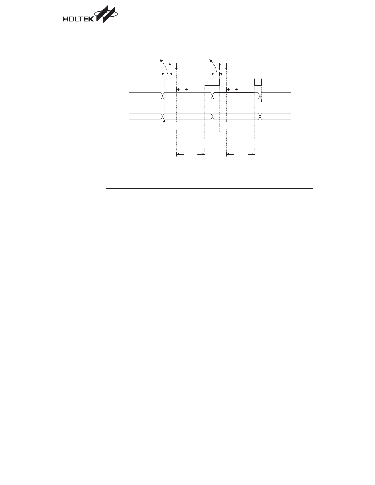
Chapter 1 Hardware Structure
The following timing diagram shows graphically the various stages involved in an analog to digital
conversion process and its associated timing.
M i n i m u m o n e i n s t r u c t i o n c y c l e n e e d e d
S T A R T
E O C B
P C R 2 ~ P C R 0
A C S 2 ~ A C S 0
Note
The Timing diagram is specified for the HT46R62/HT46C62, HT46R64/HT46C64 and HT46R65/
0 0 0 B
0 0 0 B
P o w e r - O n
R e s e t
1 : D e f i n e P B c o n f i g u r a t i o n
2 : S e l e c t a n a l o g c h a n n e l
A / D c l o c k m u s t b e f
N o t e :
HT46C65 devices. For the HT46R63/HT46C63 devices, the A/D Conversion time is 64t
of 76t
.
AD
R e s e t A / D
c o n v e r t e r
A / D s a m p l i n g t i m e
3 2 t
A D
1 0 0 B
0 1 0 B
S t a r t o f A / D
c o n v e r s i o n
E n d o f A / D
c o n v e r s i o n
7 6 t
A D
A / D c o n v e r s i o n t i m e
/ 2 , f
/ 8 o r f
S Y S
/ 3 2
S Y S
S Y S
A/D Conversion Timing
R e s e t A / D
c o n v e r t e r
A / D s a m p l i n g t i m e
3 2 t
A D
1 0 0 B
0 0 0 B
S t a r t o f A / D
c o n v e r s i o n
7 6 t
A D
A / D c o n v e r s i o n t i m e
1 . P B p o r t s e t u p a s I / O s
2 . A / D c o n v e r t e r i s p o w e r e d o f f
t o r e d u c e p o w e r c o n s u m p t i o n
d o n ' t c a r e
E n d o f A / D
c o n v e r s i o n
0 0 0 B
AD
instead
The setting up and operation of the A/D converter function is fully under the control of the application program as there are no configuration options associated with the A/D converter. After an A/D
conversion process has been initiated by the application program, the microcontroller internal
hardware will begin to carry out the conversion, during which time the program can continue with
other functions. There are two methods to determine when the A/D conversion process is complete. The first is for the application program to poll the EOCB bit in the ADCR register, while the
second method is to await an A/D internal interrupt to occur. The following two short program examples illustrate both of these methods. The example programs apply only to the HT46R62/
HT46C62, HT46R64/HT46C64 and HT46R65/HT46C65 devices which have two A/D data regis
ters. The HT46R63/HT46C63 devices have only one A/D data register as well as having a
maskable interrupt with a different EADI bit address.
Example: using EOCB Polling Method to detect end of conversion.
clr INTC0.7 ; disable A/D interrupt in interrupt control
; register
mov a,00100000B
mov ADCR,a ; setup ADCR register to configure Port PB0~PB3
; as A/D inputs and select AN0 to be connected
; to the A/D converter
mov a,00000001B
mov ACSR,a ; setup the ACSR register to select f
SYS
/8 as
; the A/D clock
75
-
Page 85

A/D with LCD Type MCU
Start_conversion:
clr ADCR.7
set ADCR.7 ; reset A/D
clr ADCR.7 ; start A/D
Polling_EOCB:
sz ADCR.6 ; poll the ADCR register EOCB bit to detect end
polling_EOCB ; continue polling
mov a,ADRH ; read conversion result from the high byte
mov adrh_buffer,a ; save result to user defined register
mov a,ADRL ; read conversion result from the low byte ADRL
mov adrl_buffer,a ; save result to user defined register
:
:
jmp start_conversion ; start next A/D conversion
Example: using Interrupt method to detect end of conversion.
set INTC0.7 ; enable A/D interrupt in interrupt control
mov a,00100000B
mov ADCR,a ; setup ADCR register to configure Port PB0~PB3
mov a,00000001B
mov ACSR,a ; setup the ACSR register to select f
start_conversion:
clr ADCR.7
set ADCR.7 ; reset A/D
clr ADCR.7 ; start A/D
:
:
; interrupt service routine
EOCB_service routine:
mov a_buffer,a ; save ACC to user defined register
mov a,ADRH ; read conversion result from the high byte
mov adrh_buffer,a ; save result to user defined register
mov a,ADRL ; read conversion result from the low byte ADRL
mov adrl_buffer,a ; save result to user defined register
clr ADCR.7
set ADCR.7 ; reset A/D
clr ADCR.7 ; start A/D
mov a,a_buffer ; restore ACC from temporary storage
reti
; of A/D conversion
; ADRH register
; register
; register
; as A/D inputs and select AN0 to be connected
; to the A/D converter
; the A/D clock
; ADRH register
; register
SYS
/8 as
76
Page 86

Chapter 1 Hardware Structure
A/D Transfer Function
As the HT46R63/HT46C63 devices contain an 8-bit A/D converter, their full-scale converted digi
tized value is equal to FF. Since the full-scale analog input value is equal to the VDD voltage, this
gives a single bit analog input value of V
which each contains a 9-bit A/D converter, their full-scale converted digitized value is equal to 1FF
giving a single bit analog input value of V
HT46R65/HT46C65 devices, which each contains a 10-bit A/D converter, their full-scale con
verted digitized value is equal to 3FF, giving a single bit analog input value of V
ing graphsshow the ideal transfer function between the analog inputvalue and the digitized output
value for the 8-bit, 9-bit and 10-bit A/D converters.
F F H
F E H
F D H
A / D C o n v e r s i o n
R e s u l t
0 3 H
0 2 H
0 1 H
1 2 3
0
Ideal A/D Transfer Function - HT46R63/HT46C63
/256. In the case of the HT46R62/HT46C62 devices
DD
/512. Similarly, the HT46R64/HT46C64 and
DD
DD
1 . 5 L S B
0 . 5 L S B
V
D D
( )
2 5 4 2 5 5 2 5 6
2 5 3
A n a l o g I n p u t V o l t a g e
2 5 6
/1024. The follow
-
-
-
A / D C o n v e r s i o n
R e s u l t
1 . 5 L S B
1 F F H
1 F E H
1 F D H
0
0 . 5 L S B
1 2 3
5 1 0 5 1 1 5 1 2
5 0 9
A n a l o g I n p u t V o l t a g e
0 3 H
0 2 H
0 1 H
Ideal A/D Transfer Function - HT46R62/HT46C62
77
V
D D
( )
5 1 2
Page 87

A/D with LCD Type MCU
1 . 5 L S B
3 F F H
3 F E H
3 F D H
A / D C o n v e r s i o n
R e s u l t
0 3 H
0 2 H
0 1 H
Ideal A/D Transfer Function - HT46R64/HT46C64 and HT46R65/HT46C65
0 . 5 L S B
V
D D
( )
1 0 2 2 1 0 2 3 1 0 2 4
1
0
2 3
1 0 2 1
A n a l o g I n p u t V o l t a g e
1 0 2 4
Interrupts
Note that to reduce the quantization error, a 0.5 LSB offset is added to the A/D Converter input. Ex
cept for the digitized value ²0², the subsequent digitized values will change at a point 0.5 LSB be
low where they would change without the offset, and the last full scale digitized value will change
at a point 1.5 LSB below the VDD.
The A/D Converter has a maximum of ±1 LSB Integral Non-Linearity Error which describes the de
parture from the ideal linear transfer function. For the HT46R63/HT46C63 devices, its 8-bit resolu
tion A/D converter is achieved with 7-bit accuracy, the 9-bit A/D resolution of the HT46R62/
HT46C62 devices is achieved with 8-bit accuracy, while the 10-bit A/D resolution of the HT46R64/
HT46C64 and HT46R65/HT46C65 devices is achieved with 9-bit accuracy.
The A/D with LCD series of microcontrollers each contains a range of both external and internal interrupt functions. The external interrupt is controlled by the action of the external pins INT0
INT1
which are present on all devices. Internal functions such as the Timer/Event Counters and
and
A/D converter all utilize the internal interrupt function for their operation.
For the A/D with LCD series of microcontroller devices, two interrupt control registers, known as
INTC0 and INTC1, are provided to control all the interrupt control features.
Once an interrupt subroutine is serviced, all the other interrupts will be blocked, by clearing the
EMI bit. This scheme may prevent any further interrupt nesting. Other interrupt requests may oc
cur during this interval but only the interrupt request flag is recorded. If another interrupt requires
servicing while the program is in the interrupt service routine, the EMI bit should be set after enter
ing theroutine, to allow interrupt nesting. If the stack is full, the interrupt request will not be acknowl
edged, evenif the related interrupt is enabled, until the Stack Pointer is decremented. If immediate
service is desired, the stack must be prevented from becoming full.
-
-
-
-
-
-
-
78
Page 88

Chapter 1 Hardware Structure
All interrupts have the capability of waking up the processor when in the HALT mode. As an inter
rupt isserviced, a control transfer occurs by pushing the Program Counter onto the stack, followed
by a branch to a subroutine at a specified location in the Program Memory. Only the Program
Counter is pushed onto the stack. If the contents of the accumulator, status register or other regis
ters are altered by the interrupt service routine, which may corrupt the desired control sequence,
then the contents should be saved in advance.
b 7 b 0
E E I 1 E E I 0 E M IE I F 0 E I F 1 E T IT FE A D I
I N T C 0 R e g i s t e r H T 4 6 R 6 2 / H T 4 6 C 6 2
M a s t e r i n t e r r u p t g l o b a l e n a b l e
1 : g l o b a l e n a b l e
0 : g l o b a l d i s a b l e
E x t e r n a l i n t e r r u p t 0 e n a b l e
1 : e n a b l e
0 : d i s a b l e
E x t e r n a l i n t e r r u p t 1 e n a b l e
1 : e n a b l e
0 : d i s a b l e
T i m e r / E v e n t C o u n t e r i n t e r r u p t e n a b l e
1 : e n a b l e
0 : d i s a b l e
E x t e r n a l i n t e r r u p t 0 r e q u e s t f l a g
1 : a c t i v e
0 : i n a c t i v e
E x t e r n a l i n t e r r u p t 1 r e q u e s t f l a g
1 : a c t i v e
0 : i n a c t i v e
T i m e r / E v e n t C o u n t e r i n t e r r u p t r e q u e s t f l a g
1 : a c t i v e
0 : i n a c t i v e
A / D C o n v e r t e r n o n - m a s k a b l e i n t e r r u p t e n a b l e
1 : e n a b l e
0 : d i s a b l e
-
-
b 7 b 0
E R T I E T B I T B FR T F
79
I N T C 1 R e g i s t e r H T 4 6 R 6 2 / H T 4 6 C 6 2
N o t i m p l e m e n t e d , r e a d a s " 0 "
T i m e B a s e i n t e r r u p t e n a b l e
1 : e n a b l e
0 : d i s a b l e
R e a l T i m e C l o c k i n t e r r u p t e n a b l e
1 : e n a b l e
0 : d i s a b l e
N o t i m p l e m e n t e d , r e a d a s " 0 "
T i m e B a s e r e q u e s t f l a g
1 : a c t i v e
0 : i n a c t i v e
R e a l T i m e C l o c k r e q u e s t f l a g
1 : a c t i v e
0 : i n a c t i v e
N o t i m p l e m e n t e d , r e a d a s " 0 "
Page 89

A/D with LCD Type MCU
b 7 b 0
b 7 b 0
T B F A D FR T F
E E I 1 E E I 0 E M IE I F 0 E I F 1 E T IT F
E R T I E A D I E T B I
I N T C 0 R e g i s t e r H T 4 6 R 6 3 / H T 4 6 C 6 3
M a s t e r i n t e r r u p t g l o b a l e n a b l e
1 : g l o b a l e n a b l e
0 : g l o b a l d i s a b l e
E x t e r n a l i n t e r r u p t 0 e n a b l e
1 : e n a b l e
0 : d i s a b l e
E x t e r n a l i n t e r r u p t 1 e n a b l e
1 : e n a b l e
0 : d i s a b l e
T i m e r / E v e n t C o u n t e r i n t e r r u p t e n a b l e
1 : e n a b l e
0 : d i s a b l e
E x t e r n a l i n t e r r u p t 0 r e q u e s t f l a g
1 : a c t i v e
0 : i n a c t i v e
E x t e r n a l i n t e r r u p t 1 r e q u e s t f l a g
1 : a c t i v e
0 : i n a c t i v e
T i m e r / E v e n t C o u n t e r i n t e r r u p t r e q u e s t f l a g
1 : a c t i v e
0 : i n a c t i v e
N o t i m p l e m e n t e d , r e a d a s " 0 "
I N T C 1 R e g i s t e r H T 4 6 R 6 3 / H T 4 6 C 6 3
T i m e B a s e i n t e r r u p t e n a b l e
1 : e n a b l e
0 : d i s a b l e
A / D C o n v e r t e r i n t e r r u p t e n a b l e
1 : e n a b l e
0 : d i s a b l e
R e a l T i m e C l o c k i n t e r r u p t e n a b l e
1 : e n a b l e
0 : d i s a b l e
N o t i m p l e m e n t e d , r e a d a s " 0 "
T i m e B a s e i n t e r r u p t r e q u e s t f l a g
1 : a c t i v e
0 : i n a c t i v e
A / D c o n v e r t e r r e q u e s t f l a g
1 : a c t i v e
0 : i n a c t i v e
R T C i n t e r r u p t r e q u e s t f l a g
1 : a c t i v e
0 : i n a c t i v e
N o t i m p l e m e n t e d , r e a d a s " 0 "
80
Page 90

Chapter 1 Hardware Structure
b 7 b 0
E E I 1 E E I 0 E M IE I F 0 E I F 1 E T 0 IT 0 FE A D I
b 7 b 0
E R T I E T B I E T 1 IT 1 F T B FR T F
I N T C 0 R e g i s t e r H T 4 6 R 6 4 / H T 4 6 C 6 4
H T 4 6 R 6 5 / H T 4 6 C 6 5
M a s t e r i n t e r r u p t g l o b a l e n a b l e
1 : g l o b a l e n a b l e
0 : g l o b a l d i s a b l e
E x t e r n a l i n t e r r u p t 0 e n a b l e
1 : e n a b l e
0 : d i s a b l e
E x t e r n a l i n t e r r u p t 1 e n a b l e
1 : e n a b l e
0 : d i s a b l e
T i m e r / E v e n t C o u n t e r 0 i n t e r r u p t e n a b l e
1 : e n a b l e
0 : d i s a b l e
E x t e r n a l i n t e r r u p t 0 r e q u e s t f l a g
1 : a c t i v e
0 : i n a c t i v e
E x t e r n a l i n t e r r u p t 1 r e q u e s t f l a g
1 : a c t i v e
0 : i n a c t i v e
T i m e r / E v e n t C o u n t e r 0 i n t e r r u p t r e q u e s t f l a g
1 : a c t i v e
0 : i n a c t i v e
A / D C o n v e r t e r n o n - m a s k a b l e i n t e r r u p t e n a b l e
1 : e n a b l e
0 : d i s a b l e
I N T C 1 R e g i s t e r H T 4 6 R 6 4 / H T 4 6 C 6 4
H T 4 6 R 6 5 / H T 4 6 C 6 5
T i m e r / E v e n t C o u n t e r 1 i n t e r r u p t e n a b l e
1 : e n a b l e
0 : d i s a b l e
T i m e B a s e i n t e r r u p t e n a b l e
1 : e n a b l e
0 : d i s a b l e
R e a l T i m e C l o c k i n t e r r u p t e n a b l e
1 : e n a b l e
0 : d i s a b l e
N o t i m p l e m e n t e d , r e a d a s " 0 "
T i m e r / E v e n t C o u n t e r 1 i n t e r r u p t r e q u e s t f l a g
1 : a c t i v e
0 : i n a c t i v e
T i m e B a s e r e q u e s t f l a g
1 : a c t i v e
0 : i n a c t i v e
R e a l T i m e C l o c k r e q u e s t f l a g
1 : a c t i v e
0 : i n a c t i v e
N o t i m p l e m e n t e d , r e a d a s " 0 "
81
Page 91

A/D with LCD Type MCU
The various interrupt enable bits, together with their associated request flags, are shown in the fol
lowing diagram with their order of priority.
A u t o m a t i c a l l y C l e a r e d b y I S R
M a n u a l l y S e t o r C l e a r e d b y S o f t w a r e
A / D C o n v e r t e r N o n - M a s k a b l e
I n t e r r u p t N o R e q u e s t F l a g
E x t e r n a l I n t e r r u p t
R e q u e s t F l a g E I F 0
E x t e r n a l I n t e r r u p t
R e q u e s t F l a g E I F 1
T i m e r / E v e n t C o u n t e r
I n t e r r u p t R e q u e s t F l a g T F
T i m e B a s e
I n t e r r u p t R e q u e s t F l a g T B F
R e a l T i m e C l o c k
I n t e r r u p t R e q u e s t F l a g R T F
A u t o m a t i c a l l y D i s a b l e d b y I S R
C a n b e E n a b l e d M a n u a l l y
E A D I
E E I 0
E E I 1
E T I
E T B I
E R T I
E M I
P r i o r i t y
H i g h
L o w
I n t e r r u p t
P o l l i n g
Interrupt Priority - HT46R62/HT46C62
A u t o m a t i c a l l y C l e a r e d b y I S R
M a n u a l l y S e t o r C l e a r e d b y S o f t w a r e
E x t e r n a l I n t e r r u p t
R e q u e s t F l a g E I F 0
A u t o m a t i c a l l y D i s a b l e d b y I S R
C a n b e E n a b l e d M a n u a l l y
E E I 0 E M I
P r i o r i t y
H i g h
-
E x t e r n a l I n t e r r u p t
R e q u e s t F l a g E I F 1
T i m e r / E v e n t C o u n t e r
I n t e r r u p t R e q u e s t F l a g T F
T i m e B a s e
I n t e r r u p t R e q u e s t F l a g T B F
A / D C o n v e r t e r
I n t e r r u p t R e q u e s t F l a g A D F
R e a l T i m e C l o c k
I n t e r r u p t R e q u e s t F l a g R T F
Interrupt Priority - HT46R63/HT46C63
82
E E I 1
E T I
E T B I
E A D I
E R T I
I n t e r r u p t
P o l l i n g
L o w
Page 92

Chapter 1 Hardware Structure
A u t o m a t i c a l l y C l e a r e d b y I S R
M a n u a l l y S e t o r C l e a r e d b y S o f t w a r e
A / D C o n v e r t e r N o n - M a s k a b l e
I n t e r r u p t N o R e q u e s t F l a g
E x t e r n a l I n t e r r u p t
R e q u e s t F l a g E I F 0
E x t e r n a l I n t e r r u p t
R e q u e s t F l a g E I F 1
T i m e r / E v e n t C o u n t e r 0
I n t e r r u p t R e q u e s t F l a g T 0 F
T i m e r / E v e n t C o u n t e r 1
I n t e r r u p t R e q u e s t F l a g T 1 F
T i m e B a s e
I n t e r r u p t R e q u e s t F l a g T B F
R e a l T i m e C l o c k
I n t e r r u p t R e q u e s t F l a g R T F
A u t o m a t i c a l l y D i s a b l e d b y I S R
C a n b e E n a b l e d M a n u a l l y
E A D I
E E I 0
E E I 1
E T 0 I
E T 1 I
E T B I
E R T I
E M I
P r i o r i t y
H i g h
L o w
I n t e r r u p t
P o l l i n g
Interrupt Priority - HT46R64/HT46C64 and HT46R65/HT46C65
Note The A/D converter interrupt for the HT46R63/HT46C63 devices is a fully maskable interrupt and
as such has an associated request flag ADF. However the A/D interrupts for the other devices are
non-maskable and therefore do not have an associated request flag.
External Interrupt
Each device in the A/D with LCD Type MCU series contains two external interrupt functions controlled byexternal pins INT0
interrupt input pins by selecting the correct configuration. In addition, the corresponding external
interrupt enable bit must be first set. These are bits 1 and 2 of the INTC0 register and known as
EEI0 and EEI1. An external interrupt is triggered by an external edge transition on one of the external interrupt pins INT0
are bits 4 and 5 of INTC0, will be set. Aconfiguration option exists for each external interrupt pin to
determine the type of external edge transition which will trigger an external interrupt. There are
four options available, low going edge, high going edge, both high and low going edge or disable.
If the disable option is chosen then the external interrupt function will be disabled and the pin will
function as a normal I/O pin. If the interrupt is enabled, the stack is not full and a logical transition,
as setup in the configuration options, occurs on either pin INT0
tion 04H or 08H respectively, will occur. The interrupt request flag EIF0 or EIF1 will be reset and
the EMI bit will be cleared to disable other interrupts.
and INT1.For an external interrupt to occur, the pins must besetup as
or INT1, after which the related interrupt request flag, EIF0 and EIF1, which
or INT1, a subroutine call to loca
83
-
Page 93

A/D with LCD Type MCU
Timer/Event Counter Interrupt
For a timer generated internal interrupt to occur, the corresponding internal interrupt enable bit
must be first set. For the devices with a single timer, this is bit 3 of the INTC0 register and is known
as ETI. For devices with two timers, the Timer 0 interrupt enable is bit 3 of the INTC0 register and
known as ET0I while the Timer 1 interrupt enable is bit 0 of the INTC1 register and known as ET1I.
An actual Timer/Event Counter interrupt will be initialized when the Timer/Event Counter interrupt
request flagis set, caused by a timer overflow. In the caseof devices with a single timer, this is bit 6
of the INTC0 register and is known as TF. In the case of devices with two timers, the Timer 0 re
quest flag is bit 6 of the INTC0 register and known as T0F, while the Timer 1 request flag is bit 4 of
the INTC1 register and known as T1F. When the master interrupt global enable bit is set, the stack
is not full and the corresponding internal interrupt enable bit is set, an internal interrupt will be gen
erated when the timer overflows. This will create a subroutine call to location 00CH for devices
with a single timer. For devices with two timers, a subroutine call to location 00CH will occur for
Timer 0 and a subroutine call to location 010H for Timer 1. When an internal interrupt occurs, the in
terrupt request flag, TF, T0F or T1F will be reset and the EMI bit will be cleared to disable other in
terrupts.
Time Base Interrupt
For a Time Base interrupt to occur the corresponding internal interrupt enable bit ETBI, must be
first set. For the HT46R63/HT46C63 devices this is bit 0 of the INTC1 register, while for the
HT46R62/HT46C62, HT46R64/HT46C64 and HT46R65/HT46C65 devices this is bit 1 of the
INTC1 register. An actual Time Base interrupt will be initialized when the Time Base interrupt re
quest flag TBF is set, a situation that will occur when a time-out signal is generated from the Time
Base. Inthe case of the HT46R63/HT46C63 devices this is bit 4 of the INTC1register, while forthe
HT46R62/HT46C62, HT46R64/HT46C64 and HT46R65/HT46C65 devices this is bit 5 of the
INTC1 register. When the master interrupt global enable bit is set, the stack is not full and the corresponding Time Base interrupt enable bit is set, an internal Time Base interrupt will be generated
when atime-out signalis generated from the Time Base. For the HT46R63/HT46C63 devices, this
will create a subroutine call to location 010H, while for the HT46R62/HT46C62, HT46R64/
HT46C64 and HT46R65/HT46C65 devices, a subroutine call to location 14H will be created.
When a Time Base interrupt occurs, the interrupt request flag TBF will be reset and the EMI bit will
be cleared to disable other interrupts.
-
-
-
-
-
The purpose of the Time Base Interrupt is to provide an interrupt signal at fixed time periods. The
Time Base Interrupt clock source originates from the internal clock source f
. This fSinput clock
S
first passes through a divider, the division ratio of which is selected by configuration options to pro
vide longer Time Base Interrupt periods. The Time Base Interrupt time-out period ranges from
12
2
/fS~215/fS. The clock source that generates fS, which in turn controls the Time Base Interrupt pe
riod, can originate from three different sources, the RTC oscillator, Watchdog Timer oscillator or
the System oscillator/4, the choice of which is determine by the f
clock source configuration op
S
tion. Note that for the HT46R62/HT46C62, HT46R64/HT46C64 and HT46R65/HT46C65 devices,
if the RTC oscillator is selected as the system clock, then f
, and correspondingly the Time Base In
S
terrupt, will also have the RTC oscillator as its clock source.
f
/ 4
S Y S
W D T O s c i l l a t o r
R T C O s c i l l a t o r
fS
S o u r c e
C o n f i g u r a t i o n
O p t i o n
f
S
C o n f i g u r a t i o n O p t i o n
D i v i d e b y 2
1 5
T i m e B a s e I n t e r r u p t
1 2
1 5
/ fS~ 2
/ f
2
S
1 2
~ 2
Time Base Interrupt
84
-
-
-
-
Page 94

Chapter 1 Hardware Structure
Real Time Clock Interrupt - RTC
For a Real Time Clock interrupt to occur the corresponding internal interrupt enable bit ERTI, must
be first set. For all the devices in the A/D with LCD Type MCU series, this is bit 2 of the INTC1 regis
ter. An actual Real Time Clock interrupt will be initialized when the Real Time Clock interrupt re
quest flagRTF is set. When the master interrupt global enable bit is set, the stack is not full and the
corresponding RealTime Clock interrupt enable bit is set,an internal Real Time Clock interrupt will
be generated when a time-out signal occurs, a subroutine call to location 018H will be created.
When a Real Time Clock interrupt occurs, the interrupt request flag RTF will be reset and the EMI
bit will be cleared to disable other interrupts. It is important not to confuse the RTC Interrupt with
the RTC oscillator.
Similar in operation to the Time Base Interrupt, the purpose of the RTC Interrupt is also to provide
an interrupt signal at fixed time periods. The RTC Interrupt clock source originates from the inter
nal clock source f
lected by programming the appropriate bits in the RTCC register to obtain longer RTC Interrupt
periods whose value ranges from 2
controls the RTC Interrupt period, can originate from three different sources, the RTC oscillator,
Watchdog Timer oscillator or the System oscillator/4, the choice of which is determine by the f
clock source configuration option. Note that for the HT46R62/HT46C62, HT46R64/HT46C64 and
HT46R65/HT46C65 devices, if the RTC oscillator is selected as the system clock, then f
respondingly the RTC Interrupt, will also have the RTC oscillator as its clock source.
. This fSinput clock first passes through a divider, the division ratio of which is se
S
8
/fS~215/fS. The clock source that generates fS, which in turn
S
f
/ 4
S Y S
W D T O s c i l l a t o r
R T C O s c i l l a t o r
fS
S o u r c e
C o n f i g u r a t i o n
O p t i o n
f
S
D i v i d e b y 28~ 2
( S e t b y R T C C
R e g i s t e r s )
1 5
R T C I n t e r r u p t
8
1 5
/ fS~ 2
/ f
2
S
, and cor
-
-
-
-
S
-
R T 2 ~ R T 0
RTC Interrupt
Note that the RTC Interrupt period is controlled by both configuration options and an internal register RTCC. A configuration option selects the source clock for the internal clock f
register bits RT2, RT1 and RT0 select the division ratio. Note that the actual division ratio can be
programmed from 2
8
to 215. For details of the actual RTC Interrupt periods, consult the RTCC reg-
ister section.
Note
After a wake-up the system requires 1024 clock cycles to resume normal operation. If the
32768Hz RTC oscillator is also selected as the system clock source, then for RTC interrupt appli
cations that are timing sensitive after a wake-up, precautions should be taken when selecting the
8,29
2
and 210RTC interrupt division. For these division ratios, after a wake-up, some following
RTC interrupt events will be missed during this 1024 clock cycle period.
A/D Interrupt
Depending upon which device is chosen there are two kinds of interrupts associated with the A/D
converter, a maskable interrupt and a non-maskable interrupt. The A/D interrupt in the
HT46R63/HT46C63 devices is similar to the other interrupts in that it is a maskable type interrupt
and has both an enable bit and a request flag. The A/D interrupt for the HT46R62/HT46C62,
HT46R64/HT46C64 and HT46R65/HT46C65 devices is different in that it is a non-maskable type
and therefore has no associated request flag.
85
, and the RTCC
S
-
Page 95

A/D with LCD Type MCU
In the HT46R63/HT46C63 devices, for an A/D interrupt to occur, the corresponding interrupt en
able bitEADI mustbe first set, which is bit 1 of the INTC1 register. An actual A/D interrupt will be ini
tialized when the A/D converter request flag ADF is set, a situation that will occur when an A/D
conversion process has completed. For the HT46R63/HT46C63 devices, this is bit 5 of the INTC1
register. When the master interrupt global bit is set, the stack is not full and the corresponding A/D
interrupt enable bit is set, an internal interrupt will be generated when the previously requested
A/D conversion process finishes. For the HT46R63/HT46C63 devices, this will create a subrou
tine call to location 14H. When an A/D interrupt occurs, the interrupt request flag ADF will be reset
and the EMI bit will be cleared to disable other interrupts.
For the HT46R62/HT46C62, HT46R64/HT46C64 and HT46R65/HT46C65 devices, which have a
non-maskable A/D interrupt, thecorresponding interruptenable bit EADI must be first set, which is
bit 7 of the INTC0 register. If the EADI bit is set, an A/D interrupt will be immediately generated
when the A/D conversion process has completed, irrespective of the condition of the EMI bit. For
the HT46R62/HT46C62, HT46R64/HT46C64 and HT46R65/HT46C65 devices, a subroutine call
to location 1CH will be created. For these devices, as no request flag is provided, and as an imme
diate jump to the interrupt subroutine address will be generated, it is important that at least one
stack level is left available if using the A/D interrupt.
Interrupt Priority
Interrupts, occurring in the interval between the rising edges of two consecutive T2 pulses, will be
serviced on the latter of the two T2 pulses, if the corresponding interrupts are enabled. In case of
simultaneous requests, the following table shows the priority that is applied. With the exception of
the A/D interrupt in the HT46R62/HT46C62, HT46R64/HT46C64 and HT46R65/HT46C65 de
vices, whichare non-maskable interrupts, these interrupts can bemasked by resetting the EMI bit.
-
-
-
-
-
Interrupt Source
External Interrupt 0 2122
External Interrupt 1 3233
TMR/TMR0 Overflow 4344
TMR1 Overflow N/A N/A 5 5
Time Base Interrupt 5466
Real Time Clock Interrupt 6677
A/D Converter Interrupt 1511
HT46R62
HT46C62
Priority
HT46R63
HT46C63
Priority
HT46R64
HT46C64
Priority
HT46R65
HT46C65
Priority
Note 1. The Timer/Event Counter 1 is available only for the HT46R64/HT46C64 and HT46R65/
HT46C65 devices as there are two Timer/Event Counters in these devices. For the HT46R62/
HT46C62 and HT46R63/HT46C63 devices, there is only one timer, known as TMR. The
HT46R64/HT46C64 and HT46R65/HT46C65 devices have two internal timers, known as
TMR0 and TMR1.
2. The HT46R62/HT46C62, HT46R64/HT46C64 andHT46R65/HT46C65 devices have non-
maskable A/D interrupt, therefore this interrupt will have priority over the others.
86
Page 96

Chapter 1 Hardware Structure
The non-maskable A/D interrupt in the HT46R62/HT46C62, HT46R64/HT46C64 and HT46R65/
HT46C65 devices will always have priority over the other interrupts. However, with the exception
of this non-maskable A/D interrupt, in cases where both external and internal interrupts are en
abled and where an external and internal interrupt occur simultaneously, the external interrupt will
always have priority and will therefore be serviced first. Suitable masking of the individual inter
rupts using the INTC0 and INTC1 registers can prevent simultaneous occurrences. The external
interrupt pins INT0
only be configured as external interrupt pins if the correct configuration option has selected them
to functionas external interrupt pins and if thecorresponding pins are programmed as input pins.
Programming Considerations
The interrupt request flags, TF, T0F, T1F, EIF0, EIF1, TBF and RTF together with the interrupt en
able bits ETI, ET0I, ET1I, EEI0, EEI1, ETBI, EADI and ERTI form the interrupt control registers
INTC0 and INTC1, which are located in the Data Memory. By disabling the interrupt enable bits, a
requested interrupt can be prevented from being serviced, however, once an interrupt request flag
is set, it will remain in this condition in the INTC0 or INTC1 register until the corresponding inter
rupt is serviced or until the request flag is cleared by a software instruction.
It is recommended that programs do not use the ²CALL subroutine² instruction within the interrupt
subroutine. Interrupts often occur in an unpredictable manner or need to be serviced immediately
in some applications. If only one stack is left and the interrupt is not well controlled, the original con
trol sequencewill be damaged once a ²CALL subroutine² is executed in the interrupt subroutine.
and INT1 are pin-shared with input pins PD4 and PD5 respectively and can
-
-
-
-
-
Reset and Initialization
A reset function is a fundamental part of any microcontroller ensuring that the device can be set to
some predetermined condition irrespective of outside parameters. The most importantreset condition is after power is first applied to the microcontroller. In this case, internal circuitry will ensure
that the microcontroller, after a short delay, will be in a well defined state and ready to execute the
first program instruction. After this power-onreset, certainimportant internal registers will be set to
defined states before the program commences. One of these registers is the Program Counter,
which will be reset to zero forcing the microcontroller to begin program execution from the lowest
Program Memory address.
In addition to the power-on reset, situations may arise where it is necessary to forcefully apply a re
set condition when the microcontroller is running. One example of this is where after power has
been applied and the microcontroller is already running, the RES
such case, known as a normal operation reset, some of the microcontroller registers remain un
changed allowing the microcontroller to proceed with normal operation after the reset line is al
lowed to return high. Another type of reset is when the Watchdog Timer overflows and resets the
microcontroller. All types of reset operations result in different register conditions being setup.
Another reset exists in the form of a Low Voltage Reset, LVR, where a full reset, similar to the RES
reset isimplemented in situations where the power supplyvoltage falls below a certain threshold.
-
line is forcefully pulled low. In
-
-
87
Page 97

A/D with LCD Type MCU
Reset
There are five ways in which a microcontroller reset can occur, through events occurring both inter
nally and externally:
Power-on Reset
®
The most fundamental and unavoidable reset is the one that occurs after power is first applied to
the microcontroller. As well as ensuring that the Program Memory begins execution from the first
memory address, a power-on reset also ensures that certain other registers are preset to known
conditions. All the I/O port and port control registers will power up in a high condition ensuring that
all pins will be first set to inputs.
Although the microcontroller has an internal RC reset function, due to unstable power on condi
tions, an external RC network connected to the RES
lay created by the RC network ensures that the RES
the power supply stabilizes. During this time, normal operation of the microcontroller is inhibited.
After the RES
line reaches a certain voltage value, the reset delay time t
an extra delay time after which the microcontroller can begin normal operation. The abbreviation
SST in the figures stands for System Start-up Timer.
pin is generally recommended. This time de
pin remains low for an extended period while
is invoked to provide
RSTD
-
-
-
V D D
R E S
S S T T i m e - o u t
I n t e r n a l R e s e t
0 . 9 V
t
D D
R S T D
Power-On Reset Timing Chart
® RES Pin Reset
This type of reset occurs when the microcontroller is already running and the RES
pulled low by external hardware such as an external switch. In this case as in the case of other reset, the Program Counter will reset to zero and program execution initiated from this point.
0 . 9 V
R E S
S S T T i m e - o u t
I n t e r n a l R e s e t
0 . 4 V
D D
t
D D
R S T D
RES Reset Timing Chart
pin is forcefully
88
Page 98

Chapter 1 Hardware Structure
Low Voltage Reset - LVR
®
With the exception of the HT46R63/HT46C63 devices, the microcontroller contains a low voltage
reset circuit in order to monitor the supply voltage of the device. If the supply voltage of the device
drops to within a range of 0.9V~V
automatically reset the device internally. The LVR includes the following specifications: For a valid
LVR signal, a low voltage, i.e. a voltage in the range between0.9V~V
1ms. If the low voltage state does not exceed 1ms, the LVR will ignore it and will not perform a re
set function.
S S T T i m e - o u t
I n t e r n a l R e s e t
Watchdog Time-out Reset during Normal Operation
®
The Watchdog Time-out Reset during normal operation is the same as RES
Watchdog Time-out flag TO will be set to ²1².
such as might occur when changing the battery, the LVR will
LVR
must existfor greater than
LVR
L V R
t
R S T D
Low Voltage Reset Timing Chart
reset except that the
-
W D T T i m e - o u t
S S T T i m e - o u t
I n t e r n a l R e s e t
t
R S T D
WDT Time-out Reset during Normal Operation Timing Chart
® Watchdog Time-out Reset during HALT
The Watchdog Time-out Reset during HALT is a little different from other kinds of reset. Most of the
conditions remain unchanged except that the Program Counter and the Stack Pointer will be
cleared to ²0² and the TO flag will be set to ²1². Refer to the A.C. Characteristics for t
W D T T i m e - o u t
t
S S T
S S T T i m e - o u t
WDT Time-out Reset during HALT Timing Chart
SST
details.
89
Page 99

A/D with LCD Type MCU
The different types of reset described affect the reset flags in different ways.These flagsknown as
and TO are located in the status register and are controlled by various microcontroller operations
such as the HALT function or Watchdog Timer. The reset flags are shown in the table:
TO RESET Conditions
0 0 RES
u u RES
1 u WDT time-out reset during normal operation
1 1 WDT time-out reset during HALT
²u² stands for unchanged
reset during power on
or LVR reset during normal operation
The table indicates the way in which the various components of the microcontroller are affected af
ter a power-on reset occurs.
Item Condition After RESET
Program Counter Reset to zero
Interrupts All interrupts will be disabled
WDT, RTC Interrupt, Time Base Clear after reset, WDT begins counting
Timer/Event Counter All Timer Counters will be turned off
Prescaler The Timer Counter Prescaler will be cleared
Input/Output Ports All I/O ports will be setup as inputs
Stack Pointer Stack pointer will point to the top of the stack
The different kinds of resets all affect the internal registers of the microcontroller in different ways.
To ensure reliable continuation of normal program execution after a reset occurs, it is important to
know what condition the microcontroller is in after a particular reset occurs. The following table describes how each type of reset affects each of the microcontroller internal registers.
-
90
Page 100

Chapter 1 Hardware Structure
HT46R62/HT46C62
Register
MP0 1xxx xxxx 1uuu uuuu 1uuu uuuu 1uuu uuuu
MP1 1xxx xxxx 1uuu uuuu 1uuu uuuu 1uuu uuuu
ACC xxxx xxxx uuuu uuuu uuuu uuuu uuuu uuuu
PCL 0000 0000 0000 0000 0000 0000 0000 0000
BP 0000 0000 0000 0000 0000 0000 uuuu uuuu
TBLP xxxx xxxx uuuu uuuu uuuu uuuu uuuu uuuu
TBLH
RTCC
STATUS
INTC0 0000 0000 0000 0000 0000 0000 uuuu uuuu
INTC1
TMR xxxx xxxx xxxx xxxx xxxx xxxx uuuu uuuu
TMRC
PA 1111 1111 1111 1111 1111 1111 uuuu uuuu
PAC 1111 1111 1111 1111 1111 1111 uuuu uuuu
PB
PBC
PD
PDC
PWM0 xxxx xxxx xxxx xxxx xxxx xxxx uuuu uuuu
PWM1 xxxx xxxx xxxx xxxx xxxx xxxx uuuu uuuu
PWM2 xxxx xxxx xxxx xxxx xxxx xxxx uuuu uuuu
ADRL
ADRH xxxx xxxx xxxx xxxx xxxx xxxx uuuu uuuu
ADCR 0100 0000 0100 0000 0100 0000 uuuu uuuu
ACSR
²u² stands for unchanged
²x² stands for unknown
²-² stands for unimplemented
Reset
(Power On)
--xx xxxx --uu uuuu --uu uuuu --uu uuuu
--00 0111 --00 0111 --00 0111 --uu uuuu
--00 xxxx --uu uuuu --1u uuuu --11 uuuu
- 00--00--00--00--00--00--uu--uu-
00- 0 1000 00- 0 1000 00- 0 1000 uu- u uuuu
--11 1111 --11 1111 --11 1111 --uu uuuu
--11 1111 --11 1111 --11 1111 --uu uuuu
- 111 - 111 - 111 - 111 - 111 - 111 - uuu - uuu
- 111 - 111 - 111 - 111 - 111 - 111 - uuu - uuu
x - - - - - - - x - - - - - - - x - - - - - - - u - - - - - - -
1 - - - - - 00 1- - - - - 00 1- - - - - 00 1- - - - - uu
RES
or LVR
Reset
WDT Time-out
(Normal Operation)
WDT Time-out
(HALT)
91
 Loading...